Flexible Pentacene Organic Thin Film Transistors using Sol-Gel ...
Flexible Pentacene Organic Thin Film Transistors using Sol-Gel ...
Flexible Pentacene Organic Thin Film Transistors using Sol-Gel ...

You also want an ePaper? Increase the reach of your titles
YUMPU automatically turns print PDFs into web optimized ePapers that Google loves.
P-19 / C. G. Choi<br />
P-19: <strong>Flexible</strong> <strong>Pentacene</strong> <strong>Organic</strong> <strong>Thin</strong> <strong>Film</strong> <strong>Transistors</strong> <strong>using</strong> <strong>Sol</strong>-<strong>Gel</strong><br />
Hybrid Polymer Gate Dielectrics<br />
Chaun Gi Choi, Seung-Yeon Kwak, and Byeong-Soo Bae<br />
Department of Materials Science and Engineering, KAIST, Daejeon 305-701, Republic of Korea<br />
Abstract<br />
<strong>Flexible</strong> organic thin film transistors (OTFTs) have been realized<br />
with sol-gel hybrid polymers (hybrimer) gate dielectric and<br />
poly(ether sulfone) substrate. The hybrimer thin films have good<br />
electrical and surface properties. OTFTs on polymer substrate<br />
exhibit good OTFT performance and small hysteresis.<br />
1. Introduction<br />
<strong>Organic</strong> thin film transistors (OTFTs) have attracted much<br />
attention because OTFTs have lots of advantages such as low cost,<br />
easy processability and flexibility. By <strong>using</strong> them, we can fabricate<br />
easily the cheap electronic devices, like integrated circuits and<br />
driving circuits for active matrix display, sensors, and RFIDs[1].<br />
Their performance has been improved impressively during the last<br />
two decades[2]. The organic dielectric is favored as the gate<br />
dielectric in OTFTs due to their solution processability and<br />
flexibility which can lower process temperature and make it easy<br />
to fabricate large-area OTFTs. However, organic gate dielectric<br />
has high leakage current densities and poor chemical stability. In<br />
addition, the organic gate dielectric causes the large hysteresis of<br />
the OTFTs.<br />
The sol-gel derived siloxane based organic-inorganic hybrid<br />
polymers (hybrimers) are nanocomposite materials in which<br />
inorganic and organic components are intimately linked at the<br />
molecular scale by a covalent bond[3,4]. Since the hybrimer<br />
combines the characteristics of both glass and polymers, the<br />
hybrimer has the good electrical and surface properties such as<br />
low leakage current density, smooth and chemically stable surface,<br />
and good photo-patternability[3,5]. In this study, we synthesized<br />
methacryl-grafted hybrimer and fabricated the hybrimer gate<br />
dielectric layer for flexible OTFTs by solution process.<br />
2. Experimental<br />
2.1 Synthesis of Hybrimer Resins and <strong>Film</strong>s<br />
The hybrimer containing oligosiloxanes grafted by methacryl<br />
radicals was synthesized <strong>using</strong> a simple non-hydrolytic sol-gel<br />
reaction. 3-(trimethoxysilyl)propyl methacrylate (MPTMS),<br />
diphenylsilanediol (DPSD) were used as precursors without<br />
further purification. The total proportion of MPTMS and DPSD<br />
together was 1 : 1 molar ratio. Barium hydroxide monohydrate<br />
(Ba(OH) 2·H 2 O, Aldrich) was used as a catalyst to promote a<br />
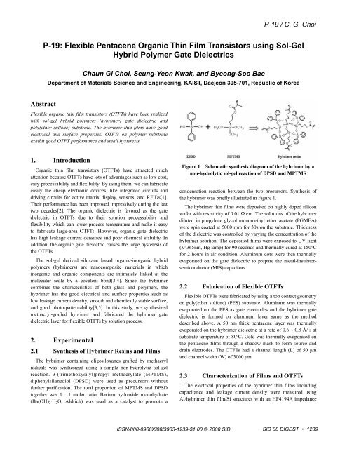
Figure 1 Schematic synthesis diagram of the hybrimer by a<br />
non-hydrolytic sol-gel reaction of DPSD and MPTMS<br />
condensation reaction between the two precursors. Synthesis of<br />
the hybrimer was briefly illustrated in Figure 1.<br />
The hybrimer thin films were deposited on highly doped silicon<br />
wafer with resistivity of 0.01 Ω cm. The solutions of the hybrimer<br />
diluted in propylene glycol monomethyl ether acetate (PGMEA)<br />
were spin coated at 5000 rpm for 30s on the substrate. Thickness<br />
of the dielectric was controlled by varying the concentration of the<br />
hybrimer solution. The deposited films were exposed to UV light<br />
(λ=365nm, Hg lamp) for 90 seconds and thermally cured at 150°C<br />
for 2 hours in air condition. Aluminum dots were then thermally<br />
evaporated on the gate dielectric to prepare the metal-insulatorsemiconductor<br />
(MIS) capacitors.<br />
2.2 Fabrication of <strong>Flexible</strong> OTFTs<br />
<strong>Flexible</strong> OTFTs were fabricated by <strong>using</strong> a top contact geometry<br />
on poly(ether sulfone) (PES) substrate. Aluminum was thermally<br />
evaporated on the PES as gate electrodes and the hybrimer gate<br />
dielectric is formed on aluminum layer same as the method<br />
described above. A 50 nm thick pentacene layer was thermally<br />
evaporated on the hybrimer dielectric at a rate of 0.6 ~ 0.8 Å/ s at<br />
substrate temperature of 80ºC. Gold was thermally evaporated on<br />
the pentacene films through a shadow mask to form source and<br />
drain electrodes. The OTFTs had a channel length (L) of 50 μm<br />
and channel width (W) of 3000 μm.<br />
2.3 Characterization of <strong>Film</strong>s and OTFTs<br />
The electrical properties of the hybrimer thin films including<br />
capacitance and leakage current density were measured <strong>using</strong><br />
Al/hybrimer thin film/Si structures with an HP4194A impedance<br />
ISSN/008-0966X/08/3903-1239-$1.00 © 2008 SID<br />
SID 08 DIGEST • 1239
P-19 / C. G. Choi<br />
analyzer and a Keithley 236 source-measure unit. The<br />
crystallographic ordering and the morphology of pentacene on the<br />
hybrimer thin films were measured <strong>using</strong> X-ray diffraction (XRD)<br />
and AFM, respectively. And contact angle analyzer was used to<br />
examine hydrophobicity of the hybrimer surface. Electrical<br />
characteristics of the OTFTs were measured <strong>using</strong> an HP 4155A<br />
semiconductor parameter analyzer.<br />
3. Results and Discussion<br />
3.1 Characteristics of Hybrimer <strong>Film</strong>s<br />
The formation of totally cross-linked 3-dimensional networks<br />
and few hydroxyl groups in the hybrimer gate insulator give the<br />
low leakage current density and high dielectric strength of the<br />
hybrimer thin film. Figure 2 shows the current densities of the<br />
hybrimer dielectric as a function of the hybrimer thin film<br />
thickness. The dielectric strength, which is measured at leakage<br />
Current density (A/cm 2 )<br />
10 -4<br />
10 -5<br />
10 -6<br />
10 -7<br />
10 -8<br />
10 -9<br />
10 -10<br />
10 -11<br />
10 -12<br />
320nm<br />
100nm<br />
80nm<br />
40nm<br />
0.0 0.5 1.0 1.5 2.0 2.5 3.0<br />
current density of 10 -6 A/cm 2 , is higher than 2.5 MV/cm. The<br />
leakage current densities at 1MV/cm increase from 4nA/cm 2 to<br />
15nA/cm 2 as the film thickness decrease. The electrical properties<br />
of the hybrimer thin films are much better than those of the<br />
commonly used polymer dielectric in OTFTs[6,7]. The dielectric<br />
constant of the hybrimer dielectric film is 3.1 at 100 kHz, which is<br />
calculated from the film thickness and capacitance.. The water<br />
contact angles of the hybrimer thin films are as high as ~80°,<br />
which indicates that they have the hydrophobic surface. It is<br />
known that surface properties such as surface energy and<br />
roughness of gate dielectric are one of the most important factors<br />
affecting the performance of the OTFTs. Figure 3 shows that the<br />
spin-coated hybrimer thin films have pin-hole free surface and<br />
their rms roughness is as low as ~0.5 nm examined by an atomic<br />
force microscopy (AFM), which reveals that the hybrimer thin<br />
films have the very smooth surface. Since the hybrimer thin films<br />
have the good electrical properties such as low leakage current<br />
densities and high dielectric strength, and the smooth and<br />
hydrophobic surface, the hybrimer can be used as the gate<br />
dielectric in OTFTs.<br />
3.2 Characteristics of Active Layer<br />
It is known that the performance of the OTFTs depends on the<br />
crystallinity and grain size of organic semiconductor[8,9]. Figure 4<br />
shows the XRD patterns of the pentacene films deposited on<br />
hybriemr gate dielectric with 50nm. The XRD patterns of the<br />
pentacene show the thin-film phase of pentacene with its main<br />
peak at 2θ =5.7°. Three characteristic peaks which come from the<br />
(00l) planes of the thin-film phase are shown in the XRD patterns.<br />
Due to the fact that the main peak is sharp and intense, a high<br />
crystallinity of pentacene on the hybrimer gate dielectric can be<br />
assumed. Also we investigated the morphology of pentacene on<br />
the hybrimer gate dielectric <strong>using</strong> AFM. Figure 5 shows AFM<br />
Figure 2<br />
Leakage current densities of the hybrimer thin films<br />
with different thickness<br />
Figure 3<br />
AFM images of spin-coated the hybrimer films.<br />
Image is 5 μm × 5 μm in size.<br />
Figure 4 X-ray diffraction patterns of the pentacene films<br />
deposited on the hybrimer gate dielectric<br />
1240 • SID 08 DIGEST
P-19 / C. G. Choi<br />
(a)<br />
-14<br />
-12<br />
-10<br />
-8<br />
20V<br />
10V<br />
0V<br />
-10V<br />
-20V<br />
-30V<br />
I D<br />
(μA)<br />
-6<br />
-4<br />
-2<br />
0<br />
Figure 5 AFM image of pentacene on the hybrimer gate<br />
dielectric. Image is 5 μm × 5 μm in size.<br />
images of the morphology of pentacene film on the hybrimer gate<br />
dielectric which has large grain size of about 1 μm. Grain size is<br />
big enough that charge carriers would flow between pentacene<br />
molecules easily.<br />
3.3 Characteristics of <strong>Flexible</strong> OTFTs<br />
Figure 6(a) shows the output curves of the flexible OTFTs with<br />
the hybrimer gate dielectric at various gate voltages (V G ). The<br />
flexible OTFTs exhibit good linear/saturation behavior. Figure<br />
6(b) shows the transfer curve of the flexible OTFTs with the<br />
hybrimer gate dielectric. The drain-source voltage (V DS ) was kept<br />
at -40 V. The gate voltage (V G ) was swept continuously with a 0.5<br />
V step, starting from +20V, passing through -40V, and finally<br />
returning to +40V. The electrical parameters were determined from<br />
a plot of I D 1/2 vs. V G on the basis of the following relationship in<br />
the saturation regime:<br />
I<br />
WC<br />
2L<br />
i<br />
2<br />
D<br />
μ(VG<br />
−Vth<br />
)<br />
= (1)<br />
(b)<br />
I D<br />
(A)<br />
10 -4<br />
10 -5<br />
10 -6<br />
10 -7<br />
10 -8<br />
10 -9<br />
10 -10<br />
10 -11<br />
10 0 -10 -20 -30 -40<br />
V DS<br />
(V)<br />
-40 -30 -20 -10 0 10 20<br />
V G<br />
(V)<br />
Figure 6 (a) Output characteristics and (b) Transfer<br />
characteristics of OTFTs with the hybrimer gate dielectric on<br />
PES [inset: photograph of the flexible OTFTs]<br />
small hysteresis is due to the hydrophobic surface and the low<br />
leakage current, and few hydroxyl groups of the gate dielectric.<br />
where I D is the drain current, μ is the field-effect mobility, C i is the<br />
capacitance per unit area, V th is the threshold voltage.<br />
The flexible OTFTs have the mobility of 0.15 cm 2 /Vs and<br />
threshold voltage of -13.4 V, respectively. The subthreshold slope,<br />
S, defined as the voltage require to increase the drain current by a<br />
factor of 10, was 2 V/decade. The on/off current ratio is higher<br />
than 10 6 , which is pretty high ratio. Furthermore, the flexible<br />
OTFTs with the hybrimer gate dielectric show small hysteresis as<br />
shown in Figure 6(b). One major problem in <strong>using</strong> solution<br />
processable gate dielectric is the hysteresis problem. It is desirable<br />
that the hysteresis of OTFTs is as small as possible for organic<br />
circuit applications. In the case of the hybrimer gate dielectric,<br />
4. Conclusion<br />
<strong>Sol</strong>ution-processed the hybrimer thin film showes good<br />
electrical properties, including high dielectric strength and low<br />
leakage current density down to the 40 nm thickness, and have<br />
also smooth and hydrophobic surface. And pentacene forms large<br />
grain with high crystallinity on the hybrimer gate dielectric. The<br />
electrical properties of the hybrimer thin film are much better than<br />
those of the commonly used polymer dielectric in OTFTs. The<br />
flexible OTFTs fabricated on the PES substrate with the hybrimer<br />
gate dielectric exhibit a mobility of 0.15 cm 2 /V s, a threshold<br />
voltage of -13.4 V, and high on/off ration of >10 5 . In addition, the<br />
SID 08 DIGEST • 1241
P-19 / C. G. Choi<br />
flexible OTFTs have small hysteresis. <strong>Sol</strong>ution-processed<br />
hybrimer gate dielectric will make it possible to fabricate the<br />
flexible and low-cost OTFTs with high-performance.<br />
5. References<br />
[1] G. H. <strong>Gel</strong>inck, H. E. Huitema, E. van Veenendaal, E. Cantatore,<br />
L. Schrijnemakers, J. B. P. H. Van Der Putten, T. C. T. Geuns,<br />
M. Beenhakkers, J. B. Giesbers, B. -H. Huisman, E. J. Meijer,<br />
E. M. Benito,F. J. Touwslager, A. W. Marsman, B. J. E. Van<br />
Rens, D. M. de Leeuw, “<strong>Flexible</strong> active-matrix displays and<br />
shift registers based on solution-processed organic transistors”,<br />
Nat. Mater. Vol. 3, p. 106, 2004<br />
[2] T.W. Kelley, L.D. Boardman, T.D. Dunbar, D.V. Muyres, M.J.<br />
Pellerite T.P. Smith, “High-Performance OTFTs Using<br />
Surface-Modified Alumina Dielectrics”, J. Phys. Chem. B Vol.<br />
107, p. 5877, 2003.<br />
[3] Y.-J. Eo, T. H.Lee, S. Y. Kim, J. K. Kang, Y. S. Han, B.-S. Bae,<br />
“Synthesis and Molecular Structure Analysis of Nano-Sized<br />
Methacryl-Grafted Polysiloxane Resin for Fabrication of Nano<br />
Hybrid Materials”, J. Polym. Sci. Part B: Polym. Phys. Vol. 43,<br />
p. 827, 2005<br />
[4] Y.J. Eo, J.H. Kim, J.H. Ko, B.S. Bae, “Optical Characteristic of<br />
Photo-Curable Methacryl -Oligosiloxane Nano Hybrid Thick<br />
<strong>Film</strong>s”, J. Mater. Res. Vol. 20, p. 401, 2005<br />
[5] C. G. Choi, B. S. Bae, “<strong>Organic</strong>–Inorganic Hybrid Materials<br />
as <strong>Sol</strong>ution Processible Gate Insulator for <strong>Organic</strong> <strong>Thin</strong> <strong>Film</strong><br />
<strong>Transistors</strong>”, Org. Electron. Vol. 8, p. 743, 2007<br />
[6] H. Klauk, M. Halik, U. Zschieschang, G. Schmid, W. Radlik,<br />
W. Weber, “High-mobility polymer gate dielectric pentacene<br />
thin film transistors”, J. Appl. Phys. Vol. 92, p. 5259, 2002<br />
[7] J. Park, S. Y. Park, S.-O. Shim, H. Kang, H. H. Lee, “A<br />
polymer gate dielectric for high-mobility polymer thin-film<br />
transistors and solvent effects”, Appl. Phys. Lett. Vol. 85, p.<br />
3283, 2004<br />
[8] D. Knipp, R. A. Street, A. Volkel, J. Ho, “Morphology and<br />
electronic transport of polycrystalline pentacene thin-film<br />
transistors”, J. Appl. Phys. Vol. 93, p. 347, 2003<br />
[9] Y. Yang, K. Shin, C. E. Park, “The Effect of Gate-Dielectric<br />
Surface Energy on <strong>Pentacene</strong> Morphology and <strong>Organic</strong> Field-<br />
Effect Transistor Characteristics”, Adv. Funct. Matter. Vol. 15,<br />
p. 1806, 2005<br />
1242 • SID 08 DIGEST