ICX414AQ - Sony
ICX414AQ - Sony
ICX414AQ - Sony

Create successful ePaper yourself
Turn your PDF publications into a flip-book with our unique Google optimized e-Paper software.
<strong>ICX414AQ</strong><br />
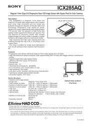
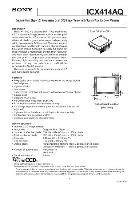
Diagonal 8mm (Type 1/2) Progressive Scan CCD Image Sensor with Square Pixel for Color Cameras<br />
Description<br />
The <strong>ICX414AQ</strong> is a diagonal 8mm (Type 1/2) interline<br />
CCD solid-state image sensor with a square pixel<br />
array suitable for VGA format. Progressive scan<br />
allows all pixel's signals to be output independently<br />
within approximately 1/60 second. This chip features<br />
an electronic shutter with variable charge-storage<br />
time which makes it possible to realize full-frame still<br />
image without a mechanical shutter. High resolution<br />
and high color reproductivity are achieved through<br />
the use of R, G, B primary color mosaic filters.<br />
Further, high sensitivity and low dark current are<br />
achieved through the adoption of HAD (Hole-<br />
Accumulation Diode) sensors.<br />
This chip is suitable for applications such as FA<br />
and surveillance cameras.<br />
Features<br />
• Progressive scan allows individual readout of the image signals<br />
from all pixels.<br />
• High sensitivity<br />
• Low smear<br />
• High vertical resolution still images without a mechanical shutter<br />
• Square pixel<br />
• Supports VGA format<br />
• Horizontal drive frequency: 24.54MHz<br />
• R, G, B primary color mosaic filters on chip<br />
• No voltage adjustments (reset gate and substrate bias are not<br />
adjusted.)<br />
• High resolution, low dark current, high color reproductivity<br />
• Continuous variable-speed shutter<br />
• Excellent anti-blooming characteristics<br />
22 pin DIP (Cer-DIP)<br />
Pin 1<br />
V<br />
2<br />
Pin 12<br />
H 31<br />
Optical black position<br />
(Top View)<br />
2<br />
8<br />
Device Structure<br />
• Interline CCD image sensor<br />
• Image size: Diagonal 8mm (Type 1/2)<br />
• Number of effective pixels: 659 (H) × 494 (V) approx. 330K pixels<br />
• Total number of pixels: 692 (H) × 504 (V) approx. 350K pixels<br />
• Chip size:<br />
7.48mm (H) × 6.15mm (V)<br />
• Unit cell size:<br />
9.9µm (H) × 9.9µm (V)<br />
• Optical black:<br />
Horizontal (H) direction: Front 2 pixels, rear 31 pixels<br />
Vertical (V) direction: Front 8 pixels, rear 2 pixels<br />
• Number of dummy bits: Horizontal 16<br />
Vertical 5<br />
• Substrate material: Silicon<br />
∗ Wfine CCD is trademark of <strong>Sony</strong> corporation.<br />
Represents a CCD adopting progressive scan, primary color filter and square pixel.<br />
<strong>Sony</strong> reserves the right to change products and specifications without prior notice. This information does not convey any license by<br />
any implication or otherwise under any patents or other right. Application circuits shown, if any, are typical examples illustrating the<br />
operation of the devices. <strong>Sony</strong> cannot assume responsibility for any problems arising out of the use of these circuits.<br />
– 1 –<br />
E02403C3Z
<strong>ICX414AQ</strong><br />
USE RESTRICTION NOTICE (December 1, 2003 ver.)<br />
This USE RESTRICTION NOTICE ("Notice") is for customers who are considering or currently using the CCD<br />
products ("Products") set forth in this specifications book. <strong>Sony</strong> Corporation ("<strong>Sony</strong>") may, at any time, modify<br />
this Notice which will be available to you in the latest specifications book for the Products. You should abide by<br />
the latest version of this Notice. If a <strong>Sony</strong> subsidiary or distributor has its own use restriction notice on the<br />
Products, such a use restriction notice will additionally apply between you and the subsidiary or distributor. You<br />
should consult a sales representative of the subsidiary or distributor of <strong>Sony</strong> on such a use restriction notice<br />
when you consider using the Products.<br />
Use Restrictions<br />
• The Products are intended for incorporation into such general electronic equipment as office products,<br />
communication products, measurement products, and home electronics products in accordance with the<br />
terms and conditions set forth in this specifications book and otherwise notified by <strong>Sony</strong> from time to time.<br />
• You should not use the Products for critical applications which may pose a life- or injury- threatening risk or<br />
are highly likely to cause significant property damage in the event of failure of the Products. You should<br />
consult your <strong>Sony</strong> sales representative beforehand when you consider using the Products for such critical<br />
applications. In addition, you should not use the Products in weapon or military equipment.<br />
• <strong>Sony</strong> disclaims and does not assume any liability and damages arising out of misuse, improper use,<br />
modification, use of the Products for the above-mentioned critical applications, weapon and military<br />
equipment, or any deviation from the requirements set forth in this specifications book.<br />
Design for Safety<br />
• <strong>Sony</strong> is making continuous efforts to further improve the quality and reliability of the Products; however,<br />
failure of a certain percentage of the Products is inevitable. Therefore, you should take sufficient care to<br />
ensure the safe design of your products such as component redundancy, anti-conflagration features, and<br />
features to prevent mis-operation in order to avoid accidents resulting in injury or death, fire or other social<br />
damage as a result of such failure.<br />
Export Control<br />
• If the Products are controlled items under the export control laws or regulations of various countries, approval<br />
may be required for the export of the Products under the said laws or regulations. You should be responsible<br />
for compliance with the said laws or regulations.<br />
No License Implied<br />
• The technical information shown in this specifications book is for your reference purposes only. The<br />
availability of this specifications book shall not be construed as giving any indication that <strong>Sony</strong> and its<br />
licensors will license any intellectual property rights in such information by any implication or otherwise. <strong>Sony</strong><br />
will not assume responsibility for any problems in connection with your use of such information or for any<br />
infringement of third-party rights due to the same. It is therefore your sole legal and financial responsibility to<br />
resolve any such problems and infringement.<br />
Governing Law<br />
• This Notice shall be governed by and construed in accordance with the laws of Japan, without reference to<br />
principles of conflict of laws or choice of laws. All controversies and disputes arising out of or relating to this<br />
Notice shall be submitted to the exclusive jurisdiction of the Tokyo District Court in Japan as the court of first<br />
instance.<br />
Other Applicable Terms and Conditions<br />
• The terms and conditions in the <strong>Sony</strong> additional specifications, which will be made available to you when you<br />
order the Products, shall also be applicable to your use of the Products as well as to this specifications book.<br />
You should review those terms and conditions when you consider purchasing and/or using the Products.<br />
– 2 –
<strong>ICX414AQ</strong><br />
Block Diagram and Pin Configuration<br />
(Top View)<br />
NC<br />
GND<br />
NC<br />
Vφ1<br />
Vφ2<br />
Vφ3<br />
NC<br />
NC<br />
11 10 9<br />
8 7 6 5 4 3 2 1<br />
Vertical register<br />
Note)<br />
Horizontal register<br />
Note)<br />
: Photo sensor<br />
15<br />
16<br />
17 18 19 20 21 22<br />
φSUB<br />
Hφ1<br />
Hφ2<br />
NC<br />
CGG<br />
VOUT<br />
R<br />
G<br />
R<br />
G<br />
G<br />
R<br />
G<br />
R<br />
G<br />
B<br />
G<br />
B<br />
G<br />
B<br />
G<br />
R<br />
G<br />
R<br />
G<br />
B<br />
G<br />
B<br />
G<br />
B<br />
R<br />
G<br />
R<br />
G<br />
12<br />
13<br />
14<br />
VDD<br />
φRG<br />
VL<br />
NC<br />
NC<br />
CSUB<br />
SUBCIR<br />
NC<br />
Pin Description<br />
Pin No. Symbol Description Pin No. Symbol Description<br />
1 NC<br />
12 VDD Supply voltage<br />
10 CGG Output amplifier gate ∗1 Supply voltage for the substrate<br />
21 SUBCIR<br />
voltage generation<br />
2<br />
3<br />
4<br />
5<br />
6<br />
7<br />
8<br />
9<br />
NC<br />
Vφ3<br />
Vφ2<br />
Vφ1<br />
NC<br />
GND<br />
NC<br />
VOUT<br />
Vertical register transfer clock<br />
Vertical register transfer clock<br />
Vertical register transfer clock<br />
GND<br />
Signal output<br />
13<br />
14<br />
15<br />
16<br />
17<br />
18<br />
19<br />
20<br />
φRG<br />
VL<br />
φSUB<br />
Hφ1<br />
Hφ2<br />
NC<br />
NC<br />
CSUB<br />
Reset gate clock<br />
Protective transistor bias<br />
Substrate clock<br />
Horizontal register transfer clock<br />
Horizontal register transfer clock<br />
Substrate bias ∗2<br />
11 NC<br />
22 NC<br />
∗1 DC bias is applied within the CCD, so that this pin should be grounded externally through a capacitance<br />
of 1µF or more.<br />
∗2 DC bias is applied within the CCD, so that this pin should be grounded externally through a capacitance<br />
of 0.1µF or more.<br />
– 3 –
<strong>ICX414AQ</strong><br />
Absolute Maximum Ratings<br />
Item<br />
Substrate clock φSUB – GND<br />
VDD, VOUT, CGG, SUBCIR – GND<br />
Supply voltage<br />
VDD, VOUT, CGG, SUBCIR – φSUB<br />
Vφ1, Vφ2, Vφ3 – GND<br />
Clock input voltage<br />
Vφ1, Vφ2, Vφ3 – φSUB<br />
Voltage difference between vertical clock input pins<br />
Voltage difference between horizongal clock input pins<br />
Hφ1, Hφ2 – Vφ3<br />
Hφ1, Hφ2 – GND<br />
Hφ1, Hφ2 – φSUB<br />
VL – φSUB<br />
Vφ2, Vφ3 – VL<br />
RG – GND<br />
Vφ1, Hφ1, Hφ2, GND – VL<br />
Storage temperature<br />
Performance guarantee temperature<br />
Operating temperature<br />
Ratings Unit Remarks<br />
–0.3 to +55 V<br />
–0.3 to +18 V<br />
–55 to +10 V<br />
–15 to +20 V<br />
to +10 V<br />
to +15 V<br />
to +17 V<br />
–16 to +16 V<br />
–10 to +15 V<br />
–55 to +10 V<br />
–65 to +0.3 V<br />
–0.3 to +27.5 V<br />
–0.3 to +22.5 V<br />
–0.3 to +17.5 V<br />
–30 to +80 °C<br />
–10 to +60 °C<br />
–10 to +75 °C<br />
∗1<br />
∗1 +27V (Max.) when clock width < 10µs, clock duty factor < 0.1%.<br />
+16V (Max.) is guaranteed for power-on and power-off.<br />
– 4 –
<strong>ICX414AQ</strong><br />
Bias Conditions<br />
Item<br />
Symbol<br />
Min.<br />
Typ.<br />
Max.<br />
Unit<br />
Remarks<br />
Supply voltage<br />
VDD<br />
14.55 15.0 15.45<br />
V<br />
Protective transistor bias<br />
VL<br />
∗1<br />
Substrate clock<br />
φSUB<br />
∗2<br />
Reset gate clock<br />
φRG<br />
∗3<br />
∗1 VL setting is the VVL voltage of the vertical transfer clock waveform, or the same voltage as the VL power<br />
supply for the V driver should be used.<br />
∗2 Indications of substrate voltage setting value<br />
Set SUBCIR pin to open when applying a DC bias the substrate clock pin.<br />
Adjust the substrate voltage because the setting value of the substrate voltage is indicated on the back of<br />
image sensor by a special code when applying a DC bias the substrate clock pin.<br />
VSUB code – two characters indication<br />
↑<br />
Integer portion<br />
↑<br />
Decimal portion<br />
The integer portion of the code and the actual value correspond to each other as follows.<br />
Integer portion of code<br />
A<br />
C<br />
d<br />
E<br />
f<br />
G<br />
h<br />
J<br />
Value<br />
5<br />
6<br />
7<br />
8<br />
9<br />
10<br />
11<br />
12<br />
[Example] "A5" → VSUB = 5.5V<br />
∗3 Do not apply a DC bias to the reset gate clock pins, because a DC bias is generated within the CCD.<br />
DC Characteristics<br />
Supply current<br />
Item<br />
Symbol<br />
IDD<br />
Min. Typ. Max. Unit Remarks<br />
4.0 7.0 9.0 mA<br />
– 5 –
<strong>ICX414AQ</strong><br />
Clock Voltage Conditions<br />
Item<br />
Symbol<br />
Min.<br />
Typ.<br />
Max.<br />
Unit<br />
Waveform<br />
Diagram<br />
Remarks<br />
Readout clock voltage<br />
VVT<br />
14.55<br />
15.0<br />
15.45<br />
V<br />
1<br />
VVH02<br />
–0.05<br />
0<br />
0.05<br />
V<br />
2<br />
VVH = VVH02<br />
VVH1, VVH2, VVH3<br />
–0.2<br />
0<br />
0.05<br />
V<br />
2<br />
VVL1, VVL2, VVL3<br />
–7.8<br />
–7.5<br />
–7.2<br />
V<br />
2<br />
VVL = (VVL1 + VVL3)/2<br />
(During 24.54MHz)<br />
Vertical transfer clock<br />
voltage<br />
VVL1, VVL2, VVL3<br />
Vφ1, Vφ2, Vφ3<br />
| VVL1 – VVL3 |<br />
–8.0<br />
6.8<br />
–7.5<br />
7.5<br />
–7.0<br />
8.05<br />
0.1<br />
V<br />
V<br />
V<br />
2<br />
2<br />
2<br />
VVL = (VVL1 + VVL3)/2<br />
(During 12.27MHz)<br />
VVHH<br />
0.5<br />
V<br />
2<br />
High-level coupling<br />
VVHL<br />
0.5<br />
V<br />
2<br />
High-level coupling<br />
VVLH<br />
0.5<br />
V<br />
2<br />
Low-level coupling<br />
VVLL<br />
0.5<br />
V<br />
2<br />
Low-level coupling<br />
Horizontal transfer<br />
clock voltage<br />
VφH<br />
VHL<br />
VCR<br />
4.75<br />
–0.05<br />
0.8<br />
5.0<br />
0<br />
2.5<br />
5.25<br />
0.05<br />
V<br />
V<br />
V<br />
3<br />
3<br />
3<br />
Cross-point voltage<br />
Reset gate clock<br />
voltage<br />
VφRG<br />
VRGLH – VRGLL<br />
VRGL – VRGLm<br />
4.5<br />
5.0<br />
5.5<br />
0.8<br />
0.5<br />
V<br />
V<br />
V<br />
4<br />
4<br />
4<br />
Low-level coupling<br />
Low-level coupling<br />
Substrate clock voltage<br />
VφSUB<br />
21.5<br />
22.5<br />
23.5<br />
V<br />
5<br />
– 6 –
<strong>ICX414AQ</strong><br />
Clock Equivalent Circuit Constants<br />
Item<br />
Symbol<br />
Min.<br />
Typ.<br />
Max.<br />
Unit<br />
Remarks<br />
CφV1<br />
3900<br />
pF<br />
Capacitance between vertical transfer clock and GND<br />
CφV2<br />
3300<br />
pF<br />
CφV3<br />
3300<br />
pF<br />
CφV12<br />
2200<br />
pF<br />
Capacitance between vertical transfer clocks<br />
CφV23<br />
2200<br />
pF<br />
CφV31<br />
1800<br />
pF<br />
Capacitance between horizontal transfer clock and GND<br />
CφH1, CφH2<br />
47<br />
pF<br />
Capacitance between horizontal transfer clocks<br />
CφHH<br />
30<br />
pF<br />
Capacitance between reset gate clock and GND<br />
CφRG<br />
6<br />
pF<br />
Capacitance between substrate clock and GND<br />
CφSUB<br />
390<br />
pF<br />
Vertical transfer clock series resistor<br />
R1, R2<br />
R3<br />
27<br />
22<br />
Ω<br />
Ω<br />
Vertical transfer clock ground resistor<br />
RGND<br />
100<br />
Ω<br />
Horizontal transfer clock series resistor<br />
RφH1, RφH2<br />
16<br />
Ω<br />
Reset gate clock series resistor<br />
RφRG<br />
39<br />
Ω<br />
Vφ1<br />
R1 R2 Vφ2<br />
CφV12<br />
CφV1<br />
RGND<br />
CφV2<br />
Hφ1<br />
RφH1<br />
CφHH<br />
RφH2<br />
Hφ2<br />
CφV31<br />
CφV3<br />
CφV23<br />
CφH1<br />
CφH2<br />
R3<br />
Vφ3<br />
Vertical transfer clock equivalent circuit<br />
Horizontal transfer clock equivalent circuit<br />
RφRG<br />
CφRG<br />
Reset gate clock equivalent circuit<br />
– 7 –
<strong>ICX414AQ</strong><br />
Drive Clock Waveform Conditions<br />
(1) Readout clock waveform<br />
VT<br />
100%<br />
90%<br />
φM<br />
10%<br />
0%<br />
tr<br />
VVT<br />
twh<br />
tf<br />
φM<br />
2<br />
0V<br />
Note) Readout clock is used by composing vertical transfer clocks Vφ2 and Vφ3.<br />
(2) Vertical transfer clock waveform<br />
Vφ1<br />
VVH1<br />
VVHH<br />
VVH<br />
VVHL<br />
VVLH<br />
VVL01<br />
VVL1<br />
VVL<br />
VVLL<br />
Vφ2<br />
VVH02<br />
VVHH<br />
VVH2<br />
VVH<br />
VVHL<br />
VVLH<br />
VVL2<br />
VVLL<br />
VVL<br />
Vφ3<br />
VVH3<br />
VVHH<br />
VVH<br />
VVHL<br />
VVL03<br />
VVLH<br />
VVL<br />
VVLL<br />
VVH = VVH02<br />
VVL = (VVL01 + VVL03)/2<br />
VVL3 = VVL03<br />
– 8 –<br />
VφV1 = VVH1 – VVL01<br />
VφV2 = VVH02 – VVL2<br />
VφV3 = VVH3 – VVL03
<strong>ICX414AQ</strong><br />
(3) Horizontal transfer clock waveform<br />
Hφ1, Hφ2<br />
tr<br />
twh<br />
tf<br />
Hφ2<br />
90%<br />
VCR<br />
10%<br />
Hφ1<br />
VφH<br />
VφH<br />
2<br />
twl<br />
VHL<br />
two<br />
Cross-point voltage for the Hφ1 rising side of the horizontal transfer clocks Hφ1 and Hφ2 waveforms is VCR.<br />
The overlap period for twh and twl of horizontal transfer clocks Hφ1 and Hφ2 is two.<br />
(4) Reset gate clock waveform<br />
φRG<br />
tr<br />
twh<br />
tf<br />
RG waveform<br />
VRGH<br />
twl<br />
VφRG<br />
Point A<br />
VRGLH<br />
VRGLL<br />
VRGLm<br />
VRGL<br />
VRGLH is the maximum value and VRGLL is the minimum value of the coupling waveform during the period from<br />
Point A in the above diagram until the rising edge of RG.<br />
In addition, VRGL is the average value of VRGLH and VRGLL.<br />
VRGL = (VRGLH + VRGLL)/2<br />
Assuming VRGH is the minimum value during the interval twh, then:<br />
VφRG = VRGH – VRGL<br />
Negative overshoot level during the falling edge of RG is VRGLm.<br />
(5) Substrate clock waveform<br />
φSUB<br />
100%<br />
90%<br />
φM<br />
10%<br />
VSUB 0%<br />
(A bias generated within the CCD)<br />
tr<br />
VφSUB<br />
twh<br />
tf<br />
φM<br />
2<br />
– 9 –
<strong>ICX414AQ</strong><br />
Clock Switching Characteristics (Horizontal drive frequency: 24.54MHz)<br />
Item<br />
Symbol<br />
twh<br />
twl tr tf<br />
Unit<br />
Min. Typ. Max. Min. Typ. Max. Min. Typ. Max. Min. Typ. Max.<br />
Remarks<br />
Readout clock<br />
VT<br />
2.3<br />
2.5<br />
0.5<br />
0.5<br />
µs<br />
During<br />
readout<br />
Vertical transfer<br />
clock<br />
Vφ1, Vφ2,<br />
Vφ3<br />
15<br />
250<br />
ns<br />
When using<br />
CXD3400N<br />
Horizontal<br />
transfer clock<br />
Hφ1<br />
Hφ2<br />
10.5 14.6<br />
10.5 14.6<br />
10.5 14.6<br />
10.5 14.6<br />
6.4<br />
6.4<br />
10.5<br />
10.5<br />
6.4<br />
6.4<br />
10.5<br />
10.5<br />
ns<br />
tf ≥ tr – 2ns<br />
Reset gate clock<br />
φRG<br />
6<br />
8<br />
25.8<br />
4<br />
3<br />
ns<br />
Substrate clock<br />
φSUB<br />
0.75<br />
0.9<br />
0.5<br />
0.5<br />
µs<br />
When draining<br />
charge<br />
Item<br />
Symbol<br />
Min.<br />
two<br />
Unit<br />
Typ. Max.<br />
Remarks<br />
Horizontal transfer clock<br />
Hφ1, Hφ2<br />
10.5 14.6<br />
ns<br />
∗1<br />
Clock Switching Characteristics (Horizontal drive frequency: 12.27MHz)<br />
Item<br />
Symbol<br />
twh<br />
twl tr tf<br />
Unit<br />
Min. Typ. Max. Min. Typ. Max. Min. Typ. Max. Min. Typ. Max.<br />
Remarks<br />
Readout clock<br />
VT<br />
4.6<br />
5.0<br />
0.5<br />
0.5<br />
µs<br />
During<br />
readout<br />
Vertical transfer<br />
clock<br />
Vφ1, Vφ2,<br />
Vφ3<br />
15<br />
350<br />
ns<br />
When using<br />
CXD3400N<br />
Horizontal<br />
transfer clock<br />
Hφ1<br />
Hφ2<br />
24 30<br />
26.5 31.5<br />
25<br />
25<br />
31.5<br />
30<br />
10<br />
10<br />
17.5<br />
15<br />
10<br />
10<br />
17.5<br />
15<br />
ns<br />
tf ≥ tr – 2ns<br />
Reset gate clock<br />
φRG<br />
11<br />
13<br />
62.5<br />
3<br />
3<br />
ns<br />
Substrate clock<br />
φSUB<br />
1.5<br />
1.8<br />
0.5<br />
0.5<br />
µs<br />
When draining<br />
charge<br />
Item<br />
Symbol<br />
Min.<br />
two<br />
Unit<br />
Typ. Max.<br />
Remarks<br />
Horizontal transfer clock<br />
Hφ1, Hφ2<br />
21.5 25.5<br />
ns<br />
∗1<br />
∗1 The overlap period of twh and twl of horizontal transfer clocks Hφ1 and Hφ2 is two.<br />
– 10 –
<strong>ICX414AQ</strong><br />
Image Sensor Characteristics<br />
(Ta = 25°C)<br />
Item<br />
Symbol<br />
Min.<br />
Typ.<br />
Max.<br />
Unit<br />
Measurement<br />
method<br />
Remarks<br />
G Sensitivity<br />
Sg<br />
670<br />
840<br />
1100<br />
mV<br />
1<br />
1/30s accumulation conversion value<br />
Sensitivity<br />
comparison<br />
Rr<br />
Rb<br />
0.4<br />
0.3<br />
0.55<br />
0.45<br />
0.7<br />
0.6<br />
1<br />
1<br />
Saturation signal<br />
Vsat<br />
500<br />
mV<br />
2<br />
Ta = 60°C<br />
Smear<br />
Sm<br />
–100<br />
–92<br />
dB<br />
3<br />
Video signal shading<br />
SHg<br />
25<br />
%<br />
4<br />
Zone 0<br />
Uniformity between<br />
video signal<br />
channels<br />
∆Srg<br />
∆Sbg<br />
8<br />
8<br />
%<br />
%<br />
5<br />
5<br />
Dark signal<br />
Vdt<br />
2<br />
mV<br />
6<br />
Ta = 60°C<br />
Dark signal shading<br />
Lag<br />
∆Vdt<br />
Lag<br />
1<br />
0.5<br />
mV<br />
%<br />
7<br />
8<br />
Ta = 60°C<br />
Note) All image sensor characteristic data noted above is for operation in 1/60s progressive scan mode.<br />
Zone Definition of Video Signal Shading<br />
659 (H)<br />
4 5<br />
4<br />
494 (V)<br />
Zone 0<br />
2<br />
Ignored region<br />
Effective pixel region<br />
Measurement System<br />
CCD signal output [ ∗ A]<br />
Gr/Gb<br />
CCD C.D.S AMP<br />
S/H<br />
R/B<br />
S/H<br />
Gr/Gb channel signal output [ ∗ B]<br />
R/B channel signal output [ ∗ C]<br />
Note) Adjust the amplifier gain so that the gain between [ ∗ A] and [ ∗ B], and between [ ∗ A] and [ ∗ C] equals 1.<br />
– 11 –
<strong>ICX414AQ</strong><br />
Image Sensor Characteristics Measurement Method<br />
Measurement conditions<br />
(1) In the following measurements, the device drive conditions are at the typical values of the bias and clock<br />
voltage conditions.<br />
(2) In the following measurements, spot blemishes are excluded and, unless otherwise specified, the optical<br />
black level (OB) is used as the reference for the signal output, which is taken as the value of the Gr/Gb<br />
channel signal output or the R/B channel signal output of the measurement system.<br />
(2) In the following measurements, this image sensor is operated in 1/60s all pixels progressive scan mode.<br />
Color coding of this image sensor & Readout<br />
Gb B Gb B<br />
R Gr R Gr<br />
Gb B Gb B<br />
The primary color filters of this image sensor are arranged in<br />
the layout shown in the figure on the left (Bayer arrangement).<br />
Gr and Gb denote the G signals on the same line as the R<br />
signal and the B signal, respectively.<br />
R Gr R Gr<br />
Horizontal register<br />
Color Coding Diagram<br />
All pixels' signals are output successively in a 1/60s period.<br />
R signal and Gr signal lines and Gb signal and B signal lines are output sequentially.<br />
– 12 –
<strong>ICX414AQ</strong><br />
Image sensor readout mode<br />
The diagram below shows the output methods for the following two readout modes.<br />
(1) Progressive scan mode<br />
R<br />
G<br />
R<br />
G<br />
R<br />
G<br />
B<br />
G<br />
B<br />
G<br />
VOUT<br />
1. Progressive scan mode<br />
In this mode, all pixel signals are output in non-interlace format in 1/60s.<br />
All pixel signals within the same exposure period are read out simultaneously, making this mode suitable for<br />
high resolution image capturing.<br />
(2) Center scan mode<br />
Undesired portions (Swept by vertical register high-speed transfer)<br />
Picture center cut-out portion<br />
2. Center scan mode<br />
This is the center scan mode using the progressive scan method.<br />
The undesired portions are swept by vertical register high-speed transfer, and the picture center portion is<br />
cut out.<br />
There are the mode (120 frames/s) which outputs 222 lines of an output line portion, and the mode<br />
(240 frames/s) which outputs 76 lines.<br />
– 13 –
<strong>ICX414AQ</strong><br />
Definition of standard imaging conditions<br />
(1) Standard imaging condition I:<br />
Use a pattern box (luminance: 706cd/m 2 , color temperature of 3200K halogen source) as a subject.<br />
(Pattern for evaluation is not applicable.) Use a testing standard lens with CM500S (t = 1.0mm) as an IR<br />
cut filter and image at F5.6. The luminous intensity to the sensor receiving surface at this point is defined<br />
as the standard sensitivity testing luminous intensity.<br />
(2) Standard imaging condition II:<br />
Image a light source (color temperature of 3200K) with a uniformity of brightness within 2% at all angles.<br />
Use a testing standard lens with CM500S (t = 1.0mm) as an IR cut filter. The luminous intensity is adjusted<br />
to the value indicated in each testing item by the lens diaphragm.<br />
1. G Sensitivity, sensitivity comparison<br />
Set to the standard imaging condition I. After setting the electronic shutter mode with a shutter speed of<br />
1/100s, measure the signal outputs (VGR, VGb, VR and VB) at the center of each Gr, Gb, R and B channel<br />
screen, and substitute the values into the following formulas.<br />
VG = (VGr + VGb)/2<br />
Sg = VG ×<br />
100<br />
[mV]<br />
30<br />
Rr = VR/VG<br />
Rb = VB/VG<br />
2. Saturation signal<br />
Set to the standard imaging condition II. After adjusting the luminous intensity to 20 times the intensity with<br />
the average value of the Gr signal output, 150mV, measure the minimum values of the Gr, Gb, R and B<br />
signal outputs.<br />
3. Smear<br />
Set to the standard imaging condition III. With the lens diaphragm at F5.6 to F8, first adjust the average<br />
value of the Gr signal output to 150mV. Measure the average values of the Gr signal output, Gb signal<br />
output, R signal output and B signal output (Gra, Gba, Ra, Ba), and then adjust the luminous intensity to<br />
500 times the intensity with the average value of the Gr signal output, 150mV.<br />
After the readout clock is stopped and the charge drain is executed by the electronic shutter at the<br />
respective H blankings, measure the maximum value (Vsm [mV]) independent of the Gr, Gb, R and B<br />
signal outputs, and substitute the values into the following formula.<br />
Sm = 20 × log ( Vsm ÷ Gra + Gba + Ra + Ba<br />
) × 1<br />
× 1<br />
4<br />
500 10<br />
[dB] (1/10V method conversion value)<br />
– 14 –
<strong>ICX414AQ</strong><br />
4. Video signal shading<br />
Set to the standard imaging condition II. With the lens diaphragm at F5.6 to F8, adjusting the luminous<br />
intensity so that the average value of the Gr signal output is 150mV. Then measure the maximum value<br />
(Grmax [mV]) and minimum value (Grmin [mV]) of the Gr signal output and substitute the values into the<br />
following formula.<br />
SHg = (Grmax – Grmin)/150 × 100 [%]<br />
5. Unifoemity between video signal channels<br />
After measuring 4, measure the maximum (Rmax [mV]) and minimum (Rmin [mV]) values of R signal, and<br />
the maximum (Bmax [mV]) and minimum (Bmin [mV]) values of B signal. Substitute the values into the<br />
following formula.<br />
∆Srg = (Rmax – Rmin )/150 × 100 [%]<br />
∆Sbg = (Bmax – Bmin )/150 × 100 [%]<br />
6. Dark signal<br />
Measure the average value of the signal output (Vdt [mV]) with the device ambient temperature of 60°C<br />
and the device in the light-obstructed state, using the horizontal idle transfer level as a reference.<br />
7. Dark signal shading<br />
After measuring 6, measure the maximum (Vdmax [mV]) and minimum (Vdmin [mV]) values of the dark<br />
signal output and substitute the values into the following formula.<br />
∆Vdt = Vdmax – Vdmin [mV]<br />
8. Lag<br />
Adjust the Gr signal output value generated by the strobe light to 150mV. After setting the strobe light so<br />
that it strobes with the following timing, measure the residual signal amount (Vlag). Substitute the value<br />
into the following formula.<br />
Lag = (Vlag/150) × 100 [%]<br />
VD<br />
V2<br />
Strobe light<br />
timing<br />
Light<br />
Gr signal output 150mV<br />
Vlag(lag)<br />
Output<br />
– 15 –
Drive Circuit<br />
15V<br />
100k<br />
0.1<br />
0.1<br />
–7.5V<br />
3.3V<br />
1<br />
20<br />
1/35V<br />
XSUB<br />
2<br />
19<br />
1/10V<br />
– 16 –<br />
XV3<br />
XSG3<br />
XV2<br />
XSG2<br />
XV1<br />
3<br />
4<br />
5<br />
6<br />
7<br />
8<br />
9<br />
10<br />
CXD3400N<br />
18<br />
17<br />
16<br />
15<br />
14<br />
13<br />
12<br />
11<br />
0.1<br />
0.1<br />
1 2 3 4 5 6 7 8<br />
NC<br />
NC<br />
NC<br />
SUBCIR<br />
Vφ3<br />
CSUB<br />
Vφ2<br />
NC<br />
Vφ1<br />
NC<br />
GND<br />
NC<br />
ICX414<br />
(BOTTOM VIEW)<br />
NC<br />
Hφ2<br />
Hφ1<br />
φSUB<br />
22 21 20 19 18 17 16 15<br />
9 10 11<br />
VOUT<br />
VL<br />
CGG<br />
φRG<br />
NC<br />
VDD<br />
14 13 12<br />
3.3/20V<br />
2SC4250<br />
4.7k<br />
0.01<br />
CCD<br />
OUT<br />
Hφ2<br />
0.1 2200p 3.3/16V<br />
1M<br />
Hφ1<br />
φRG<br />
0.1<br />
<strong>ICX414AQ</strong>
<strong>ICX414AQ</strong><br />
Spectral Sensitivity Characteristics (Excludes lens characteristics and light source characteristics)<br />
1.0<br />
0.8<br />
B<br />
G<br />
R<br />
Relative Response<br />
0.6<br />
0.4<br />
0.2<br />
0<br />
400 450 500 550 600 650 700<br />
Wave Length [nm]<br />
– 17 –
7<br />
1<br />
525<br />
510<br />
508<br />
7<br />
8<br />
1<br />
2<br />
3<br />
4<br />
5<br />
6<br />
494<br />
1<br />
2<br />
<strong>ICX414AQ</strong><br />
Drive Timing Chart (Vertical Sync) Progressive Scan Mode<br />
VD<br />
"a"<br />
HD<br />
7<br />
1<br />
525<br />
510<br />
V1<br />
– 18 –<br />
V2<br />
V3<br />
1<br />
2<br />
3<br />
4<br />
5<br />
6<br />
7<br />
8<br />
1<br />
2<br />
3<br />
494<br />
1<br />
2<br />
OUT
Drive Timing Chart (Vertical Sync "a" Enlarged) Progressive Scan Mode/Center Scand Mode<br />
"a" Enlarged<br />
H1<br />
V1<br />
V2<br />
520 582<br />
V3<br />
– 19 –<br />
121212121212 62 50<br />
121212121212<br />
<strong>ICX414AQ</strong>
Drive Timing Chart (Horizontal Sync) Progressive Scan Mode<br />
780<br />
1<br />
CLK<br />
1<br />
35<br />
1<br />
107<br />
123<br />
125<br />
H1<br />
72<br />
1<br />
16<br />
H2<br />
SHP<br />
SHD<br />
– 20 –<br />
V1<br />
1<br />
36<br />
1<br />
36<br />
V2<br />
1<br />
12 1 36<br />
1<br />
24<br />
V3<br />
1<br />
24<br />
1 36 1<br />
12<br />
SUB<br />
1<br />
37 1 23<br />
1<br />
12<br />
RG<br />
<strong>ICX414AQ</strong>
<strong>ICX414AQ</strong><br />
Drive Timing Chart (Vertical Sync) Center Scan Mode 1<br />
VD<br />
"d" "a" "b" "c"<br />
"d" "a" "b"<br />
HD<br />
261<br />
262<br />
12345678<br />
246<br />
245<br />
24<br />
20<br />
21<br />
261<br />
262<br />
12345678<br />
246<br />
245<br />
V1<br />
– 21 –<br />
V2<br />
V3<br />
1<br />
356<br />
357<br />
136<br />
137<br />
1<br />
356<br />
357<br />
OUT
Drive Timing Chart (Horizontal Sync) Center Scan Mode 1 (Frame Shift) ("b")<br />
10920 bits = 14H<br />
35<br />
107<br />
H1<br />
H2<br />
– 22 –<br />
V1<br />
V2<br />
V3<br />
121212121212 121212121212<br />
#1<br />
#142<br />
<strong>ICX414AQ</strong>
Drive Timing Chart (Horizontal Sync) Center Scan Mode 1 (High-speed Sweep) ("d")<br />
12480 bits = 16H<br />
35<br />
107<br />
H1<br />
H2<br />
– 23 –<br />
V1<br />
V2<br />
V3<br />
121212121212 121212121212<br />
#1<br />
#167<br />
<strong>ICX414AQ</strong>
<strong>ICX414AQ</strong><br />
Drive Timing Chart (Vertical Sync) Center Scan Mode 2<br />
VD<br />
"d" "a" "b" "c"<br />
"d" "a" "b"<br />
HD<br />
130<br />
131<br />
12345678<br />
129<br />
106<br />
105<br />
30<br />
27<br />
26<br />
129<br />
130<br />
131<br />
12345678<br />
106<br />
105<br />
V1<br />
– 24 –<br />
V2<br />
V3<br />
1<br />
283<br />
284<br />
209<br />
210<br />
1<br />
283<br />
284<br />
OUT
Drive Timing Chart (Horizontal Sync) Center Scan Mode 2 (Frame Shift) ("b")<br />
15600 bits = 20H<br />
35<br />
107<br />
H1<br />
H2<br />
– 25 –<br />
V1<br />
V2<br />
V3<br />
121212121212 121212121212<br />
#1<br />
#215<br />
<strong>ICX414AQ</strong>
Drive Timing Chart (Horizontal Sync) Center Scan Mode 2 (High-speed Sweep) ("d")<br />
18720 bits = 24H<br />
35<br />
107<br />
H1<br />
H2<br />
– 26 –<br />
V1<br />
V2<br />
V3<br />
121212121212 121212121212<br />
#1<br />
#255<br />
<strong>ICX414AQ</strong>
<strong>ICX414AQ</strong><br />
Notes on Handling<br />
1) Static charge prevention<br />
CCD image sensors are easily damaged by static discharge. Before handling be sure to take the following<br />
protective measures.<br />
a) Either handle bare handed or use non-chargeable gloves, clothes or material.<br />
Also use conductive shoes.<br />
b) When handling directly use an earth band.<br />
c) Install a conductive mat on the floor or working table to prevent the generation of static electricity.<br />
d) Ionized air is recommended for discharge when handling CCD image sensor.<br />
e) For the shipment of mounted substrates, use boxes treated for the prevention of static charges.<br />
2) Soldering<br />
a) Make sure the package temperature does not exceed 80°C.<br />
b) Solder dipping in a mounting furnace causes damage to the glass and other defects. Use a 30W<br />
soldering iron with a ground wire and solder each pin in less than 2 seconds. For repairs and remount,<br />
cool sufficiently.<br />
c) To dismount an image sensor, do not use a solder suction equipment. When using an electric desoldering<br />
tool, use a thermal controller of the zero cross On/Off type and connect it to ground.<br />
3) Dust and dirt protection<br />
Image sensors are packed and delivered by taking care of protecting its glass plates from harmful dust and<br />
dirt. Clean glass plates with the following operation as required, and use them.<br />
a) Perform all assembly operations in a clean room (class 1000 or less).<br />
b) Do not either touch glass plates by hand or have any object come in contact with glass surfaces. Should<br />
dirt stick to a glass surface, blow it off with an air blower. (For dirt stuck through static electricity ionized<br />
air is recommended.)<br />
c) Clean with a cotton bud and ethyl alcohol if the grease stained. Be careful not to scratch the glass.<br />
d) Keep in a case to protect from dust and dirt. To prevent dew condensation, preheat or precool when<br />
moving to a room with great temperature differences.<br />
e) When a protective tape is applied before shipping, just before use remove the tape applied for<br />
electrostatic protection. Do not reuse the tape.<br />
4) Installing (attaching)<br />
a) Remain within the following limits when applying a static load to the package. Do not apply any load more<br />
than 0.7mm inside the outer perimeter of the glass portion, and do not apply any load or impact to limited<br />
portions. (This may cause cracks in the package.)<br />
Upper ceramic<br />
39N<br />
29N<br />
29N<br />
0.9Nm<br />
Lower ceramic<br />
Low melting<br />
point glass<br />
Compressive strength<br />
Shearing strength<br />
Tensile strength<br />
Torsional stregth<br />
b) If a load is applied to the entire surface by a hard component, bending stress may be generated and the<br />
package may fracture, etc., depending on the flatness of the ceramic portions. Therefore, for installation,<br />
use either an elastic load, such as a spring plate, or an adhesive.<br />
– 27 –
<strong>ICX414AQ</strong><br />
c) The adhesive may cause the marking on the rear surface to disappear, especially in case the regulated<br />
voltage value is indicated on the rear surface. Therefore, the adhesive should not be applied to this area,<br />
and indicated values should be transferred to other locations as a precaution.<br />
d) The notch of the package is used for directional index, and that can not be used for reference of fixing.<br />
In addition, the cover glass and seal resin may overlap with the notch of the package.<br />
e) If the leads are bent repeatedly and metal, etc., clash or rub against the package, the dust may be<br />
generated by the fragments of resin.<br />
f) Acrylate anaerobic adhesives are generally used to attach CCD image sensors. In addition, cyanoacrylate<br />
instantaneous adhesives are sometimes used jointly with acrylate anaerobic adhesives.<br />
(reference)<br />
5) Others<br />
a) Do not expose to strong light (sun rays) for long periods, as color filters will be discolored. When high<br />
luminous objects are imaged with the exposure level controlled by the electronic iris, the luminance of the<br />
image-plane may become excessive and discoloring of the color filter will possibly be accelerated. In such<br />
a case, it is advisable that taking-lens with the automatic-iris and closing of the shutter during the poweroff<br />
mode should be properly arranged. For continuous using under cruel condition exceeding the normal<br />
using condition, consult our company.<br />
b) Exposure to high temperature or humidity will affect the characteristics. Accordingly avoid storage or<br />
usage in such conditions.<br />
c) Brown stains may be seen on the bottom or side of the package. But this does not affect the CCD<br />
characteristics.<br />
– 28 –
Package Outline Unit: mm<br />
22 pin DIP (600mil)<br />
0.7<br />
A<br />
9.0<br />
22 12<br />
0˚ to 9˚<br />
12<br />
22<br />
B<br />
~ ~<br />
3<br />
3<br />
11.55<br />
7.55<br />
V<br />
H<br />
15.1 ± 0.3<br />
15.24<br />
C<br />
2-R0.7<br />
– 29 –<br />
0.55<br />
1<br />
18.0 ± 0.4<br />
11 1<br />
17.6<br />
B'<br />
14.6<br />
3<br />
0.7<br />
3.26 ± 0.3<br />
0.25<br />
1. "A" is the center of the effective image area.<br />
2. The two points "B"of the package are the horizontal reference.<br />
The point "B"of the package is the vertical reference.<br />
0.69<br />
0.3<br />
(For the 1st.pin only)<br />
1.27 0.46<br />
1.27<br />
4.0 ± 0.3<br />
3 The bottom "C"of the package is the height reference.<br />
4 The center of the effective image area,relative to "B"and "B'"is<br />
H V 9.0 7.55 ± 0.15mm<br />
0.3 M<br />
5 The rotation angle of the effective image area relative to H and V is ± 1˚<br />
6 The height from bottom "C" to the effective image area is 1.41 ± 0.15mm<br />
PACKAGE MATERIAL<br />
Cer-DIP<br />
7 The tilt of the effective image area relative to the bottom "C" is less than 60µm<br />
<strong>Sony</strong> Corporation<br />
LEAD TREATMENT<br />
LEAD MATERIAL<br />
PACKAGE MASS<br />
DRAWING NUMBER<br />
TIN PLATING<br />
42 ALLOY<br />
2.60g<br />
AS-B15-03(E)<br />
8 The thickness of the cover glass is 0.75mm,and the refractive index is 1.5.<br />
9 The notches on the bottom must not be used for reference of fixing.<br />
<strong>ICX414AQ</strong>

![PDF [4833KB] - Sony](https://img.yumpu.com/26420643/1/190x235/pdf-4833kb-sony.jpg?quality=85)