Design of a side-band-separating heterodyne mixer for band 9 of ...
Design of a side-band-separating heterodyne mixer for band 9 of ...
Design of a side-band-separating heterodyne mixer for band 9 of ...

You also want an ePaper? Increase the reach of your titles
YUMPU automatically turns print PDFs into web optimized ePapers that Google loves.
<strong>Design</strong> <strong>of</strong> a <strong>side</strong>-<strong>band</strong>-<strong>separating</strong> <strong>heterodyne</strong> <strong>mixer</strong><br />
<strong>for</strong> <strong>band</strong> 9 <strong>of</strong> ALMA.<br />
F. P. Mena ∗ , J. Kooi † , A. M. Baryshev ∗ , C. F. J. Lodewijk ‡ , and W. Wild ∗<br />
∗ Space Research Organization <strong>of</strong> The Netherlands and Kapteyn Institute<br />
University <strong>of</strong> Groningen, Landleven 12, 9747 AD Groningen, The Netherlands<br />
† Cali<strong>for</strong>nia Institute <strong>of</strong> Technology, MS 320-47 Pasadena, Cali<strong>for</strong>nia 91125, USA<br />
‡ Kavli Institute <strong>of</strong> Nanoscience<br />
Delft University <strong>of</strong> Technology, Lorentzweg 1, 2628 CJ Delft, The Netherlands<br />
Abstract— A <strong>side</strong>-<strong>band</strong>-<strong>separating</strong> (SBS) <strong>heterodyne</strong> <strong>mixer</strong> has<br />
been designed <strong>for</strong> the Atacama Large Millimeter Array (ALMA)<br />
602-720 GHz <strong>band</strong>, as it will present a great improvement over<br />
the current double-<strong>side</strong>-<strong>band</strong> configuration under developed at<br />
the moment. Here we present design details and the results <strong>of</strong><br />
extensive computer simulations <strong>of</strong> its per<strong>for</strong>mance. The designed<br />
SBS <strong>mixer</strong> exploits waveguide technology. At its core it consists<br />
<strong>of</strong> a quadrature hybrid, two LO injectors, and three dumping<br />
loads. The entire structure has been analyzed in a linear circuit<br />
simulator with custom code written to accurately (verified by<br />
HFSS finite element simulations) model the hybrid structures.<br />
This technique permitted an optimization <strong>of</strong> the dimensions<br />
and the study <strong>of</strong> the consequences <strong>of</strong> deviations from the ideal<br />
situation. It is estimated that the tolerances in several <strong>of</strong> the<br />
components should be kept at less than 3 µm. Important parts<br />
<strong>of</strong> the design are the dumping loads which, due to the involved<br />
dimensions, are not easy to implement. There<strong>for</strong>e, we have also<br />
designed a simple load which is rather large compared with<br />
the waveguide making it relatively easy to realize at such small<br />
dimensions. It consists <strong>of</strong> a large cavity at the end <strong>of</strong> the<br />
waveguide and filled with an absorbing material. A simulation<br />
<strong>of</strong> its per<strong>for</strong>mance shows that be<strong>side</strong>s its simplicity it can have a<br />
reflectivity as low as -40 dB if the appropriate material is used.<br />
I. INTRODUCTION<br />
A well known improvement over double-<strong>side</strong>-<strong>band</strong> (DSB)<br />
<strong>mixer</strong>s is the <strong>side</strong>-<strong>band</strong> <strong>separating</strong> (SBS) configuration. Contrary<br />
to to the DSB <strong>mixer</strong>s, the later permits the separate<br />
detection <strong>of</strong> the upper and lower RF <strong>band</strong> frequencies. Despite<br />
this important advantage, it is not always implemented at<br />
high frequencies as the involved dimensions <strong>for</strong> the required<br />
components are prohibitory small. This is particularly true in<br />
the range corresponding to ALMA <strong>band</strong> 9 (602-720 GHz) and,<br />
hence, DSB <strong>mixer</strong>s are currently being developed. However,<br />
the current state-<strong>of</strong>-the-art technology is such that, we believe,<br />
it will permit the implementation <strong>of</strong> SBS <strong>heterodyne</strong> <strong>mixer</strong>s<br />
at even these high frequencies. We, there<strong>for</strong>e, have designed<br />
a <strong>heterodyne</strong> <strong>mixer</strong> in the SBS configuration containing a<br />
quadrature hybrid. The proposed waveguide structure has been<br />
extensively modeled assuming perfect load terminations. This<br />
modeling has permitted an optimization <strong>of</strong> the structure dimensions<br />
<strong>for</strong> the range corresponding to ALMA <strong>band</strong> 9. Deviations<br />
from the optimal dimensions have also been studied, which<br />
suggest that <strong>for</strong> a good per<strong>for</strong>mance the tolerances <strong>of</strong> several<br />
<strong>of</strong> the components have to be kept at around 3 µm. Moreover,<br />
in this article, we also propose a new design <strong>for</strong> the waveguide<br />
RF<br />
90°<br />
hybrid<br />
load<br />
SIS<br />
-3 dB, 0°<br />
-3 dB, 90°<br />
LO<br />
-3 dB, 0°<br />
power<br />
splitter<br />
-3 dB, 0°<br />
(a)<br />
LO injection<br />
(2x)<br />
LO<br />
injection<br />
-9dB<br />
LO<br />
injection<br />
-9dB<br />
Power<br />
splitter (1x)<br />
(b)<br />
Load<br />
(3x)<br />
load<br />
LO<br />
load<br />
SIS<br />
SIS<br />
Quadrature<br />
hybrid (1x)<br />
IF<br />
IF<br />
RF<br />
SIS<br />
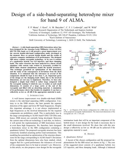
Fig. 1. (a) Diagram <strong>of</strong> the chosen configuration <strong>for</strong> a SBS <strong>mixer</strong>. (b) Core<br />
<strong>of</strong> the proposed waveguide implementation. The transversal dimensions <strong>of</strong> the<br />
waveguide are 145 × 310 µm.<br />
termination loads that will be an important component <strong>of</strong> the<br />
hybrid <strong>mixer</strong>. A new design <strong>for</strong> the loads is necessary due to<br />
the small dimensions involved. We show that with this new<br />
design a reflectivity as low as -40 dB can be achieved if the<br />
appropriate material is used.<br />
A. Quadrature Hybrid<br />
II. DESIGN<br />
A layout <strong>of</strong> the chosen configuration and the proposed implementation<br />
<strong>for</strong> the SBS <strong>mixer</strong> are shown in Fig. 1. The core<br />
<strong>of</strong> the suggested <strong>mixer</strong> consists <strong>of</strong> a quadrature hybrid, two<br />
LO injectors, and three dumping loads. Although a balanced
e<br />
d1L<br />
d W<br />
c 1L<br />
(a)<br />
145<br />
Input<br />
500 c<br />
W<br />
c 2L<br />
L<br />
a<br />
310<br />
(b)<br />
Fig. 2. Proposed design <strong>for</strong> a waveguide load (all dimensions are in µm). At<br />
the end <strong>of</strong> the waveguide, a large cavity is built which, in turn, is partially filled<br />
with an absorbing material (gray lines). The figure also shows the parameters<br />
that have been changed during the simulations.<br />
TABLE I<br />
PARAMETERS OF THE LORENTZ OSCILLATOR USED TO SIMULATE THE<br />
TRANSMISSION DATA OF REF. [2].<br />
ɛ ∞ ω o ω p γ<br />
- GHz GHz GHz<br />
4.2 15300 14220 207900<br />
<strong>mixer</strong> containing a 180 ◦ hybrid has superior fundamental<br />
and intermodulation product suppression capabilities, its 90 ◦<br />
counterpart is simpler and, thus, easier to implement at this<br />
frequencies [1].<br />
B. Load<br />
The load presented here consists <strong>of</strong> a cavity at the end <strong>of</strong><br />
the waveguide and which is partially filled with an absorbing<br />
material. The design is depicted in Fig. 2 where the space<br />
filled with the absorbing material is represented by gray lines.<br />
This geometry should be relatively easy to make as the the<br />
largest dimensions are designed to be parallel to the splitting<br />
plane <strong>of</strong> the block. Moreover, the dimensions <strong>of</strong> the load itself<br />
are suitable to be machined by conventional means.<br />
One candidate to be used as absorbing material is the<br />
commercially available epoxy MF112 [2], [3]. From published<br />
transmittance data [2], we have modeled its dielectric function<br />
in this frequency range with one Lorentz oscillator [4]. The<br />
corresponding parameters (presented in Table I) were used in<br />
the simulations presented in the following section.<br />
A. Quadrature Hybrid<br />
III. SIMULATION AND RESULTS<br />
The construction presented in Fig. 1 has been analyzed in a<br />
linear circuit simulator with custom code written to accurately<br />
model the hybrid structures. The results were verified by HFSS<br />
finite element simulations. This has the advantage that the<br />
effect <strong>of</strong> non-ideal termination impedances may be examined.<br />
In the ideal situation, the SIS junctions are well matched to<br />
Fig. 3. (a) Electric field distribution with the signal port excited. The input<br />
signal is split 50% with a 90 ◦ phase difference between the two output ports.<br />
By design approximately 10% <strong>of</strong> the LO signal is coupled into the signal path.<br />
(b) Electric field distribution with the LO port excited. Approximately 10%<br />
<strong>of</strong> the available LO power couples to the <strong>mixer</strong> path, with the remaining 90%<br />
<strong>of</strong> the LO terminated. In both cases the simulation frequency is 660 GHz.<br />
the probe impedance and the waveguide terminations are ideal.<br />
This maybe regarded as an ”upper per<strong>for</strong>mance limit”. In the<br />
non-ideal situation the port mismatch is chosen to be 25% (-12<br />
dB return loss).<br />
The results <strong>of</strong> the simulations are summarized in Figures 3<br />
through 5. First, to illustrate how the various components <strong>of</strong><br />
the proposed hybrid per<strong>for</strong>m in the ideal situation, in Fig. 3<br />
we show the electric field distributions when (a) the signal<br />
and (b) the LO ports are excited independently. In the <strong>for</strong>mer<br />
case, the input signal is split 50% with a 90 ◦ phase difference<br />
between the two output ports. By design approximately 10%<br />
<strong>of</strong> the LO signal is coupled into the signal path, and it follows<br />
from reciprocity that 90% <strong>of</strong> the signal will couple to the LO<br />
path (dump). The loss <strong>of</strong> 10% was deemed acceptable. When<br />
the LO port is excited, approximately 10% <strong>of</strong> the available<br />
LO power couples to the <strong>mixer</strong> path, with the remaining 90%<br />
<strong>of</strong> the LO terminated. It has to be noted that the device will<br />
operate at 4 K.<br />
Figure 4 shows the <strong>side</strong><strong>band</strong> rejection ratio in the ideal<br />
(upper limit) and non-ideal situations (lower limit). Note that<br />
the latter case although includes power and phase imbalances,<br />
it does not include IF and <strong>mixer</strong> gain imbalances. Finally,
(a)<br />
-2 0<br />
d W<br />
= c W<br />
& c 2 L<br />
= e d 1 L<br />
= 0 & a L<br />
= 3 1 0 µm<br />
-3 0<br />
S 1 1<br />
[d B ]<br />
-4 0<br />
-5 0<br />
(a )<br />
c W<br />
= 1 0 0 0<br />
c W<br />
= 1 5 0 0<br />
c W<br />
= 2 0 0 0<br />
c W<br />
= 2 5 0 0<br />
(b)<br />
-2 0<br />
d W<br />
= c W<br />
= 1 5 0 0 µm & a L<br />
= 3 1 0 µm & e d 1 L<br />
= 0<br />
-3 0<br />
S 1 1<br />
[d B ]<br />
-4 0<br />
-5 0<br />
(b )<br />
c 2 L<br />
= 0<br />
c 2 L<br />
= 1 0 0<br />
c 2 L<br />
= 3 0 0<br />
c 2 L<br />
= 5 0 0<br />
5 5 0 6 0 0 6 5 0 7 0 0 7 5 0<br />
f [G H z ]<br />
Fig. 4. Side<strong>band</strong> rejection ratio in the (a) ideal and (a) non-ideal situations.<br />
In the non-ideal scenario, the SIS junction and waveguide termination are<br />
presumed to be mismatched by 25% (Return loss = -12 dB). The results<br />
include power and phase imbalances, however do not include IF and <strong>mixer</strong><br />
gain imbalances.<br />
(a)<br />
(b)<br />
Fig. 5. RF and LO coupling to the SIS junctions in the (a) ideal and (b)<br />
non-ideal cases.<br />
Fig. 6. Resulting S 11 coefficient when the dimensions (a) c W and (b) c 2L<br />
are varied.<br />
Fig. 5 presents the RF and LO coupling to the SIS junctions<br />
in both cases. The LO power coupling balance is critically<br />
dependent on both LO dumps having the same termination<br />
impedance. In turn this will affect the pumping level <strong>of</strong> the<br />
individual <strong>mixer</strong>s and their <strong>mixer</strong> gain (<strong>mixer</strong> gains ought to<br />
be closely matched).<br />
B. Load<br />
The one-port system depicted in Fig. 2 was simulated in<br />
CST Microwave Studio [5] with the load material simulated<br />
according the parameters given in Table I. The geometrical<br />
parameters varied during the simulations are length <strong>of</strong> the load<br />
cavity (c W ), cavity width (d W ), height <strong>of</strong> the load (a L ), and<br />
matching between the waveguide and the load material (e d1L ).<br />
All <strong>of</strong> them are also shown in Fig. 2. In the first place, by<br />
varying c W and d W (with a L = 310 and c 2L = e d1L = 0), we<br />
have found that the overall lowest reflectivity is achieved when<br />
c W = d W = 1500 µm (Fig. 6a). At that values, the reflectivity<br />
shows a series <strong>of</strong> oscillations that are rapidly washed out by<br />
increasing c 2L (Fig. 6b).<br />
Our load design is prone to two kinds <strong>of</strong> errors, air gaps<br />
(a L < 310 µm) and geometrical mismatches between the<br />
waveguide and the load (e d1L ≠ 0). These errors have been<br />
simulated and the results are presented in Fig. 7a. The load<br />
per<strong>for</strong>mance is not degraded substantially in the presence <strong>of</strong><br />
large air gaps. As shown in Fig. 7a, a gap as large as half<br />
the waveguide height, still produces a reflectivity bellow -20<br />
dB. Regarding the geometrical mismatch e d1L , small changes
S 1 1<br />
[d B ]<br />
-2 0<br />
-3 0<br />
-4 0<br />
-5 0<br />
(a )<br />
d W<br />
= c W<br />
= 1 5 0 0 µm & c 2 L<br />
= 5 0 0 µm<br />
a L<br />
= 1 5 5 & e d 1 L<br />
= 0<br />
a L<br />
= 2 1 7 & e d 1 L<br />
= 0<br />
a L<br />
= 3 1 0 & e d 1 L<br />
= 0<br />
a L<br />
= 3 1 0 & e d 1 L<br />
= -5<br />
a L<br />
= 3 1 0 & e d 1 L<br />
= 5<br />
REFERENCES<br />
[1] J. W. Kooi, A. Kovacs, B. Bumble, G. Chattopadhyay, M. L. Edgar,<br />
S. Kaye, R. LeDuc, J. Zmuidzinas, and T. G. Phillips, Heterodyne<br />
Instrumentation Upgrade at the Caltech Submillimeter Observatory.<br />
[2] G. A. Ediss, A. R. Kerr, H. Moseley, and K. P. Stewart, ”FTS Measurements<br />
<strong>of</strong> Eccosorb MF112 at Room Temperature and 5 K from 300<br />
GHz to 2.4 THz”, ALMA Memo 273, 2 September 1999.<br />
[3] http://www.eccosorb.com/.<br />
[4] F. P. Mena and A. Baryshev, ”<strong>Design</strong> and Simulation <strong>of</strong> a Waveguide<br />
Load <strong>for</strong> ALMA-<strong>band</strong> 9”, ALMA Memo 513, 5 January 2005.<br />
[5] http://www.sonnetusa.com/.<br />
[6] Private communication, Radiometer Physics GmbH,<br />
http://www.radiometer-physics.de.<br />
S 1 1<br />
[d B ]<br />
-2 0<br />
-3 0<br />
-4 0<br />
ε 0<br />
= 5 .1<br />
ε 0<br />
= 1 0<br />
ε 0<br />
= 3 0<br />
-5 0<br />
(b )<br />
5 5 0 6 0 0 6 5 0 7 0 0 7 5 0<br />
f [G H z ]<br />
Fig. 7. Simulation <strong>of</strong> the load per<strong>for</strong>mance when : (a) mounting errors<br />
(a L < a; e d1L ≠ 0) are present and (b) different materials are used.<br />
in both directions produce a rather large degradation <strong>of</strong> the<br />
per<strong>for</strong>mance <strong>of</strong> the load. However, errors as large as 20 µm<br />
produce still a reflectivity below -20 dB (not shown here).<br />
Finally, we have modeled the per<strong>for</strong>mance <strong>of</strong> the load with<br />
different materials. This have been simulated by changing<br />
the Lorentz model given in Table I. The specific parameter<br />
changed is the static value <strong>of</strong> the dielectric function (ɛ 0 ≡<br />
ɛ(0) = ɛ ∞ + ω2 p<br />
). Fig. 7b shows the results that demonstrate<br />
ω0<br />
2<br />
the ability <strong>of</strong> our design to per<strong>for</strong>m efficiently with a wide<br />
range <strong>of</strong> materials.<br />
IV. CONCLUSIONS<br />
In conclusion we have presented a design <strong>for</strong> a <strong>side</strong>-<strong>band</strong><strong>separating</strong><br />
<strong>mixer</strong> <strong>for</strong> the frequency region corresponding to<br />
ALMA <strong>band</strong> 9. Its ideal and non-ideal properties have been<br />
presented from which it is estimated that tolerances in some<br />
<strong>of</strong> the components should be as low as 3 µm. We think these<br />
tolerances are achievable with state-<strong>of</strong>-the-art micromachining,<br />
which is confirmed by the first promising attempts [6]. A<br />
design <strong>of</strong> a new load has also been presented. Its relatively<br />
large dimensions respect to the waveguide make it appropriate<br />
<strong>for</strong> high frequencies. Moreover, the results <strong>of</strong> the simulations<br />
indicate that the design is very robust as can tolerate rather<br />
large mounting errors and a wide variety <strong>of</strong> absorbing materials.