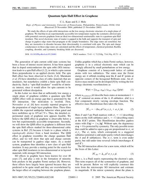
Quantum Spin Hall Effect in Graphene - APS Link Manager ...
Quantum Spin Hall Effect in Graphene - APS Link Manager ...
Quantum Spin Hall Effect in Graphene - APS Link Manager ...

You also want an ePaper? Increase the reach of your titles
YUMPU automatically turns print PDFs into web optimized ePapers that Google loves.
PRL 95, 226801 (2005)<br />
PHYSICAL REVIEW LETTERS week end<strong>in</strong>g<br />
25 NOVEMBER 2005<br />
<strong>Quantum</strong> <strong>Sp<strong>in</strong></strong> <strong>Hall</strong> <strong>Effect</strong> <strong>in</strong> <strong>Graphene</strong><br />
C. L. Kane and E. J. Mele<br />
Dept. of Physics and Astronomy, University of Pennsylvania, Philadelphia, Pennsylvania 19104, USA<br />
(Received 29 November 2004; published 23 November 2005)<br />
We study the effects of sp<strong>in</strong> orbit <strong>in</strong>teractions on the low energy electronic structure of a s<strong>in</strong>gle plane of<br />
graphene. We f<strong>in</strong>d that <strong>in</strong> an experimentally accessible low temperature regime the symmetry allowed sp<strong>in</strong><br />
orbit potential converts graphene from an ideal two-dimensional semimetallic state to a quantum sp<strong>in</strong> <strong>Hall</strong><br />
<strong>in</strong>sulator. This novel electronic state of matter is gapped <strong>in</strong> the bulk and supports the transport of sp<strong>in</strong> and<br />
charge <strong>in</strong> gapless edge states that propagate at the sample boundaries. The edge states are nonchiral, but<br />
they are <strong>in</strong>sensitive to disorder because their directionality is correlated with sp<strong>in</strong>. The sp<strong>in</strong> and charge<br />
conductances <strong>in</strong> these edge states are calculated and the effects of temperature, chemical potential, Rashba<br />
coupl<strong>in</strong>g, disorder, and symmetry break<strong>in</strong>g fields are discussed.<br />
DOI: 10.1103/PhysRevLett.95.226801 PACS numbers: 73.43. f, 72.25.Hg, 73.61.Wp, 85.75. d<br />
The generation of sp<strong>in</strong> current solid state systems has<br />
been a focus of <strong>in</strong>tense recent <strong>in</strong>terest. It has been argued<br />
that <strong>in</strong> doped semiconductors the sp<strong>in</strong> orbit (SO) <strong>in</strong>teraction<br />
leads to a sp<strong>in</strong> <strong>Hall</strong> effect [1,2], <strong>in</strong> which a sp<strong>in</strong> current<br />
flows perpendicular to an applied electric field. The sp<strong>in</strong><br />
<strong>Hall</strong> effect has been observed <strong>in</strong> GaAs [3,4]. Murakami<br />
et al. [5] have identified a class of cubic materials that are<br />
<strong>in</strong>sulators, but nonetheless exhibit a f<strong>in</strong>ite sp<strong>in</strong> <strong>Hall</strong> conductivity.<br />
Such a ‘‘sp<strong>in</strong> <strong>Hall</strong> <strong>in</strong>sulator’’ would be of <strong>in</strong>tr<strong>in</strong>sic<br />
<strong>in</strong>terest, s<strong>in</strong>ce it would allow for sp<strong>in</strong> currents to be<br />
generated without dissipation.<br />
In this Letter we show that at sufficiently low energy a<br />
s<strong>in</strong>gle plane of graphene exhibits a quantum sp<strong>in</strong> <strong>Hall</strong><br />
(QSH) effect with an energy gap that is generated by the<br />
SO <strong>in</strong>teraction. Our motivation is twofold. First,<br />
Novoselov et al. [6] have recently reported progress <strong>in</strong><br />
the preparation of s<strong>in</strong>gle layer graphene films. These films<br />
exhibit the expected ambipolar behavior when gated and<br />
have mobilities up to 10 4 cm 2 =Vs. Thus, the detailed experimental<br />
study of graphene now appears feasible. We<br />
believe the QSH effect <strong>in</strong> graphene is observable below a<br />
low but experimentally accessible temperature. Secondly,<br />
we will show the QSH effect <strong>in</strong> graphene is different from<br />
the sp<strong>in</strong> <strong>Hall</strong> effects studied for three-dimensional cubic<br />
systems <strong>in</strong> Ref. [5] because it leads to a phase which is<br />
topologically dist<strong>in</strong>ct from a band <strong>in</strong>sulator. The QSH<br />
effect <strong>in</strong> graphene resembles the charge quantum <strong>Hall</strong><br />
effect, and we will show that sp<strong>in</strong> and charge currents<br />
can be transported <strong>in</strong> gapless edge states. As a model<br />
system, graphene thus identifies a new class of sp<strong>in</strong> <strong>Hall</strong><br />
<strong>in</strong>sulator. It may provide a start<strong>in</strong>g po<strong>in</strong>t for the search for<br />
other sp<strong>in</strong> <strong>Hall</strong> <strong>in</strong>sulators <strong>in</strong> two-dimensional or <strong>in</strong> layered<br />
materials with stronger SO <strong>in</strong>teraction.<br />
SO effects <strong>in</strong> graphite have been known for over 40<br />
years [7], and play a role <strong>in</strong> the formation of m<strong>in</strong>ority<br />
hole pockets <strong>in</strong> the graphite Fermi surface [8]. However,<br />
these effects have largely been ignored because they are<br />
predicted to be quite small and they are overwhelmed by<br />
the larger effect of coupl<strong>in</strong>g between the graphene planes.<br />
Unlike graphite which has a f<strong>in</strong>ite Fermi surface, however,<br />
graphene is <strong>in</strong> a critical electronic state which can be<br />
strongly affected by small perturbations at low energy.<br />
<strong>Graphene</strong> consists of a honeycomb lattice of carbon<br />
atoms with two sublattices. The states near the Fermi<br />
energy are orbitals resid<strong>in</strong>g near the K and K 0 po<strong>in</strong>ts at<br />
opposite corners of the hexagonal Brillou<strong>in</strong> zone. An effective<br />
mass model can be developed [9] by writ<strong>in</strong>g the low<br />
energy electronic wavefunctions as<br />
r u AK ;u BK ; u AK 0;u BK<br />
0 r (1)<br />
where u A;B K;K<br />
0 r describe basis states at momentum k<br />
K, K 0 centered on atoms of the A, B sublattice. r is a<br />
four component slowly vary<strong>in</strong>g envelope function. The<br />
effective mass Hamiltonian then takes the form,<br />
H 0 i@v F y x z@ x y @ y : (2)<br />
Here ~ and ~ are Pauli matrices with z 1 describ<strong>in</strong>g<br />
states on the A B sublattice and z 1 describ<strong>in</strong>g states<br />
at the K K 0 po<strong>in</strong>ts. This Hamiltonian describes gapless<br />
states with E q v F jqj. Without sp<strong>in</strong>, the degeneracy<br />
at q 0 is protected by symmetry. The only possible terms<br />
that could be added to open a gap are proportional to z or<br />
z z. The z term, which corresponds to a staggered<br />
sublattice potential is odd under parity (which <strong>in</strong>terchanges<br />
the A and B sublattices). The z z term is even under<br />
parity, but odd under time reversal (which <strong>in</strong>terchanges K<br />
and K 0 ).<br />
The SO <strong>in</strong>teraction allows for a new term, which will be<br />
the focus of this Letter:<br />
H SO so y z zs z : (3)<br />
Here s z is a Pauli matrix represent<strong>in</strong>g the electron’s sp<strong>in</strong>.<br />
This term respects all of the symmetries of graphene, and<br />
will be present. Below we will explicitly construct this<br />
term from the microscopic SO <strong>in</strong>teraction and estimate<br />
its magnitude. If the mirror symmetry about the plane is<br />
0031-9007=05=95(22)=226801(4)$23.00 226801-1 © 2005 The American Physical Society
PRL 95, 226801 (2005)<br />
PHYSICAL REVIEW LETTERS week end<strong>in</strong>g<br />
25 NOVEMBER 2005<br />
preserved then this is the only allowed sp<strong>in</strong> dependent term<br />
at q 0. If the mirror symmetry is broken (either by a<br />
perpendicular electric field or by <strong>in</strong>teraction with a substrate)<br />
then a Rashba term [10] of the form s p ^z is<br />
allowed,<br />
H R R y x zs y y s x : (4)<br />
For R 0, so leads to an energy gap 2 so with E q<br />
p<br />
@v F q 2 2 so. For 0 < R < so the energy gap<br />
2 so R rema<strong>in</strong>s f<strong>in</strong>ite. For R > so the gap closes,<br />
and the electronic structure is that of a zero gap semiconductor<br />
with quadradically dispers<strong>in</strong>g bands. In the follow<strong>in</strong>g<br />
we will assume that R < so and analyze the<br />
properties of the result<strong>in</strong>g gapped phase. This assumption<br />
is justified by numerical estimates given at the end of the<br />
Letter.<br />
The gap generated by z zs z is different from the gap<br />
that would be generated by the staggered sublattice potentials,<br />
z or zs z . The ground states <strong>in</strong> the presence of the<br />
latter terms are adiabatically connected to simple <strong>in</strong>sulat<strong>in</strong>g<br />
phases at strong coupl<strong>in</strong>g where the two sublattices are<br />
decoupled. In contrast, the gap parameter z zs z produces<br />
gaps with opposite signs at the K and K 0 po<strong>in</strong>ts. This has no<br />
simple strong coupl<strong>in</strong>g limit. To connect smoothly between<br />
the states generated by z and z zs z one must pass<br />
through a critical po<strong>in</strong>t where the gap vanishes, separat<strong>in</strong>g<br />
ground states with dist<strong>in</strong>ct topological orders.<br />
The <strong>in</strong>teraction (3) is related to a model <strong>in</strong>troduced<br />
by Haldane [11] as a realization of the parity anomaly <strong>in</strong><br />
2 1 -dimensional relativistic field theory. Taken separately,<br />
the Hamiltonians for the s z 1 sp<strong>in</strong>s violate time<br />
reversal symmetry and are equivalent to Haldane’s model<br />
for sp<strong>in</strong>less electrons, which could be realized by <strong>in</strong>troduc<strong>in</strong>g<br />
a periodic magnetic field with no net flux. As Haldane<br />
showed, this gives rise to a z z gap, which has opposite<br />
signs at the K and K 0 po<strong>in</strong>ts. At temperatures well below<br />
the energy gap this leads to a quantized <strong>Hall</strong> conductance<br />
xy e 2 =h. This <strong>Hall</strong> conductance computed by the<br />
Kubo formula can be <strong>in</strong>terpreted as the topological Chern<br />
number <strong>in</strong>duced by the Berry’s curvature <strong>in</strong> momentum<br />
space [12,13]. S<strong>in</strong>ce the signs of the gaps <strong>in</strong> (3) are<br />
opposite for opposite sp<strong>in</strong>s, an electric field will <strong>in</strong>duce<br />
opposite currents for the opposite sp<strong>in</strong>s, lead<strong>in</strong>g to a sp<strong>in</strong><br />
current J s @=2e J " J # characterized by a quantized<br />
sp<strong>in</strong> <strong>Hall</strong> conductivity<br />
s<br />
xy<br />
e<br />
2 : (5)<br />
S<strong>in</strong>ce sp<strong>in</strong> currents do not couple to experimental probes it<br />
is difficult to directly measure (5). Moreover, the conservation<br />
of s z will be violated by the Rashba term (4) as well<br />
as terms which couple the and orbitals. Nonetheless,<br />
Murakami et al. [14] have def<strong>in</strong>ed a conserved sp<strong>in</strong> s z c ,<br />
allow<strong>in</strong>g<br />
s xy to be computed via the Kubo formula. We<br />
f<strong>in</strong>d that<br />
s xy computed <strong>in</strong> this way is not quantized when<br />
226801-2<br />
R 0, though the correction to (5) is small due to carbon’s<br />
weak SO <strong>in</strong>teraction.<br />
In the quantum <strong>Hall</strong> effect the bulk topological order<br />
requires the presence of gapless edge states. We now show<br />
that gapless edge states are also present <strong>in</strong> graphene. We<br />
will beg<strong>in</strong> by establish<strong>in</strong>g the edge states for R 0. We<br />
will then argue that the gapless edge states persist even<br />
when R 0, and that they are robust aga<strong>in</strong>st weak<br />
electron-electron <strong>in</strong>teractions and disorder. Thus, <strong>in</strong> spite<br />
of the violation of (5) the gapless edge states characterize a<br />
state which is dist<strong>in</strong>ct from an ord<strong>in</strong>ary <strong>in</strong>sulator. This QSH<br />
state is different from the <strong>in</strong>sulators discussed <strong>in</strong> Ref. [5],<br />
which do not have edge states. It is also dist<strong>in</strong>ct from the<br />
sp<strong>in</strong> <strong>Hall</strong> effect <strong>in</strong> doped GaAs, which does not have an<br />
energy gap.<br />
For R 0, the Hamiltonian (2) and (3) conserves s z ,<br />
and the gapless edge states follow from Laughl<strong>in</strong>’s argument<br />
[15]. Consider a large cyl<strong>in</strong>der (larger than @v F = so )<br />
and adiabatically <strong>in</strong>sert a quantum h=e of magnetic<br />
flux quantum down the cyl<strong>in</strong>der (slower than so=@). The<br />
result<strong>in</strong>g azimuthal Faraday electric field <strong>in</strong>duces a sp<strong>in</strong><br />
current such that sp<strong>in</strong> @ is transported from one end of the<br />
cyl<strong>in</strong>der to the other. S<strong>in</strong>ce an adiabatic change <strong>in</strong> the<br />
magnetic field cannot excite a particle across the energy<br />
gap so it follows that there must be gapless states at each<br />
end to accommodate the extra sp<strong>in</strong>.<br />
An explicit description of the edge states requires a<br />
model that gives the energy bands throughout the entire<br />
Brillou<strong>in</strong> zone. Follow<strong>in</strong>g Haldane [11], we <strong>in</strong>troduce a<br />
second neighbor tight b<strong>in</strong>d<strong>in</strong>g model,<br />
H<br />
X X<br />
tc y i c j it 2 ij s z c y i c j : (6)<br />
hiji<br />
hhijii<br />
The first term is the usual nearest neighbor hopp<strong>in</strong>g term.<br />
The second term connects second neighbors with a sp<strong>in</strong><br />
dependent amplitude. ij ji 1, depend<strong>in</strong>g on the<br />
orientation of the two nearest neighbor bonds d 1 and d 2 the<br />
electron traverses <strong>in</strong> go<strong>in</strong>g from site j to i. ij 1 ( 1)<br />
if the electron makes a left (right) turn to get to the second<br />
bond. The sp<strong>in</strong> dependent term can be written <strong>in</strong> a coord<strong>in</strong>ate<br />
<strong>in</strong>dependent representation as i d 1 d 2 p<br />
s.Atlow<br />
energy (6) reduces to (2) and (3) with so 3 3 t2 .<br />
The edge states can be seen by solv<strong>in</strong>g (7) <strong>in</strong> a strip<br />
geometry. Figure 1 shows the one-dimensional energy<br />
bands for a strip where the edges are along the zigzag<br />
direction <strong>in</strong> the graphene plane. The bulk band gaps at<br />
the one-dimensional projections of the K and K 0 po<strong>in</strong>ts are<br />
clearly seen. In addition two bands traverse the gap, connect<strong>in</strong>g<br />
the K and K 0 po<strong>in</strong>ts. These bands are localized at<br />
the edges of the strip, and each band has degenerate copies<br />
for each edge. The edge states are not chiral s<strong>in</strong>ce each<br />
edge has states which propagate <strong>in</strong> both directions.<br />
However, as illustrated <strong>in</strong> Fig. 2 the edge states are ‘‘sp<strong>in</strong><br />
filtered’’ <strong>in</strong> the sense that electrons with opposite sp<strong>in</strong><br />
propagate <strong>in</strong> opposite directions. Similar edge states occur<br />
for armchair edges, though <strong>in</strong> that case the 1D projections
PRL 95, 226801 (2005)<br />
1<br />
E/t<br />
0<br />
-1<br />
0 π/a k 2π/a<br />
FIG. 1. (a) One-dimensional energy bands for a strip of graphene<br />
(shown <strong>in</strong> <strong>in</strong>set) modeled by (7) with t 2 =t 0:03. The<br />
bands cross<strong>in</strong>g the gap are sp<strong>in</strong> filtered edge states.<br />
PHYSICAL REVIEW LETTERS week end<strong>in</strong>g<br />
25 NOVEMBER 2005<br />
X<br />
X<br />
226801-3<br />
of K and K 0 are both at k 0. It is <strong>in</strong>terest<strong>in</strong>g to note that<br />
for zigzag edges the edge states persist for so ! 0, where<br />
they become perfectly flat [16]. This leads to an enhanced<br />
density of states at the Fermi energy associated with zigzag<br />
edges. This has been recently seen <strong>in</strong> scann<strong>in</strong>g tunnel<strong>in</strong>g<br />
spectroscopy of graphite surfaces [17].<br />
We have also considered a nearest neighbor Rashba<br />
term, of the form i^z s d c y i c j . This violates the<br />
conservation of s z , so that the Laughl<strong>in</strong> argument no longer<br />
applies. Nonetheless, we f<strong>in</strong>d that the gapless edge states<br />
rema<strong>in</strong>, provided R < so , so that the bulk band gap<br />
rema<strong>in</strong>s <strong>in</strong>tact. The cross<strong>in</strong>g of the edge states at the<br />
Brillou<strong>in</strong> zone boundary k x =a <strong>in</strong> Fig. 1 (or at k 0<br />
for the armchair edge) is protected by time reversal symmetry.<br />
The two states at k x =a form a Kramers doublet<br />
whose degeneracy cannot be lifted by any time reversal<br />
symmetric perturbation. Moreover, the degenerate states at<br />
k x =a q are a Kramers doublet. This means that<br />
elastic backscatter<strong>in</strong>g from a random potential is forbidden.<br />
More generally, scatter<strong>in</strong>g from a region of disorder<br />
can be characterized by a 2 2 unitary S matrix which<br />
relates the <strong>in</strong>com<strong>in</strong>g and outgo<strong>in</strong>g states: out S <strong>in</strong> ,<br />
where is a two component sp<strong>in</strong>or consist<strong>in</strong>g of the left<br />
and right mov<strong>in</strong>g edge states L", R#. Under time reversal<br />
<strong>in</strong>;out ! s y out;<strong>in</strong><br />
. Time reversal symmetry therefore imposes<br />
the constra<strong>in</strong>t S s y S T s y , which rules out any off<br />
diagonal elements.<br />
Electron <strong>in</strong>teractions can lead to backscatter<strong>in</strong>g. For<br />
<strong>in</strong>stance, the term u y L" @ x y L" R#@ x R# , does not violate<br />
time reversal, and will be present <strong>in</strong> an <strong>in</strong>teract<strong>in</strong>g<br />
Hamiltonian. For weak <strong>in</strong>teractions this term is irrelevant<br />
under the renormalization group, s<strong>in</strong>ce its scal<strong>in</strong>g dimension<br />
is 4. It thus will not lead to an energy gap or to<br />
localization. Nonetheless, it allows <strong>in</strong>elastic backscatter<strong>in</strong>g.<br />
To lead<strong>in</strong>g order <strong>in</strong> u it gives a f<strong>in</strong>ite conductivity of<br />
the edge states, which diverges at low temperature as<br />
u 2 T 3 2 [18]. S<strong>in</strong>ce elastic backscatter<strong>in</strong>g is prevented<br />
by time reversal there are no relevant backscatter<strong>in</strong>g processes<br />
for weak <strong>in</strong>teractions. This stability aga<strong>in</strong>st <strong>in</strong>teractions<br />
and disorder dist<strong>in</strong>guishes the sp<strong>in</strong> filtered edge<br />
states from ord<strong>in</strong>ary one-dimensional wires, which are<br />
localized by weak disorder.<br />
A parallel magnetic field H k breaks time reversal and<br />
leads to an avoided cross<strong>in</strong>g of the edge states. H k also<br />
reduces the symmetry, allow<strong>in</strong>g terms <strong>in</strong> the Hamiltonian<br />
which provide a cont<strong>in</strong>uously gapped path connect<strong>in</strong>g the<br />
states generated by z zs z and z. Thus <strong>in</strong> addition to<br />
gapp<strong>in</strong>g the edge states H k elim<strong>in</strong>ates the topological<br />
dist<strong>in</strong>ction between the QSH phase and a simple <strong>in</strong>sulator.<br />
The sp<strong>in</strong> filtered edge states have important consequences<br />
for both the transport of charge and sp<strong>in</strong>. In the limit of<br />
low temperature we may ignore the <strong>in</strong>elastic backscatter<strong>in</strong>g<br />
processes, and describe the ballistic transport <strong>in</strong> the<br />
edge states with<strong>in</strong> a Landauer-Büttiker [19] framework.<br />
For a two term<strong>in</strong>al geometry [Fig. 2(a)], we predict a<br />
ballistic two term<strong>in</strong>al charge conductance G 2e 2 =h.<br />
For the sp<strong>in</strong> filtered edge states the edge current density<br />
is related to the sp<strong>in</strong> density, s<strong>in</strong>ce both depend on n R"<br />
n L# . Thus the charge current is accompanied by sp<strong>in</strong> accumulation<br />
at the edges. The <strong>in</strong>terplay between charge and<br />
sp<strong>in</strong> can be probed <strong>in</strong> a multiterm<strong>in</strong>al device. Def<strong>in</strong>e the<br />
multiterm<strong>in</strong>al sp<strong>in</strong> conductance by Ii<br />
s P<br />
jG s ij V j. Time<br />
reversal symmetry requires G s ji G s ij , and from<br />
Fig. 2(b) it is clear that G s ij e=4 for adjacent contacts<br />
i and j. In the four term<strong>in</strong>al geometry of Fig. 2(b) a sp<strong>in</strong><br />
current I s eV=4 flows <strong>in</strong>to the right contact. This<br />
geometry can also be used to measure a sp<strong>in</strong> current. A<br />
sp<strong>in</strong> current <strong>in</strong>cident from the left (<strong>in</strong>jected, for <strong>in</strong>stance,<br />
V<br />
I<br />
(a)<br />
V/2<br />
0 I s<br />
0<br />
-V/2<br />
(b)<br />
FIG. 2. Schematic diagrams show<strong>in</strong>g (a) two term<strong>in</strong>al and<br />
(b) four term<strong>in</strong>al measurement geometries. In (a) a charge<br />
current I 2e 2 =h V flows <strong>in</strong>to the right lead. In (b) a sp<strong>in</strong><br />
current I s e=4 V flows <strong>in</strong>to the right lead. The diagrams to<br />
the right <strong>in</strong>dicate the population of the edge states.<br />
0
PRL 95, 226801 (2005)<br />
PHYSICAL REVIEW LETTERS week end<strong>in</strong>g<br />
25 NOVEMBER 2005<br />
with a ferromagnetic contact) will be split, with the up<br />
(down) sp<strong>in</strong>s transported to the top (bottom) contacts,<br />
generat<strong>in</strong>g a measurable sp<strong>in</strong> <strong>Hall</strong> voltage.<br />
The magnitude of so may be estimated by treat<strong>in</strong>g the<br />
microsopic SO <strong>in</strong>teraction<br />
@<br />
V SO<br />
4m 2 s rV p (7)<br />
c2 <strong>in</strong> first order degenerate perturbation theory. We thus<br />
evaluate the expectation value of (8) <strong>in</strong> the basis of states<br />
given <strong>in</strong> (1) treat<strong>in</strong>g r as a constant. A full evaluation<br />
depends on the detailed form of the Bloch functions. However<br />
a simple estimate can be made <strong>in</strong> the ‘‘first star’’<br />
P<br />
p<br />
approximation: u K;K 0 ; A;B r p exp iK p r d = 3 .<br />
Here K p are the crystal momenta at the three corners of the<br />
Brillou<strong>in</strong> zone equivalent to K or K 0 , and d is the a basis<br />
vector from a hexagon center to an A or B sublattice site.<br />
We f<strong>in</strong>d that the matrix elements have precisely the structure<br />
(3), and us<strong>in</strong>g the Coulomb <strong>in</strong>teraction V r e 2 =r we<br />
estimate 2 so 4 2 e 2 @ 2 = 3m 2 c 2 a 3 2:4K. This is a<br />
crude estimate, but it is comparable to the SO splitt<strong>in</strong>gs<br />
quoted <strong>in</strong> the graphite literature [8].<br />
The Rashba <strong>in</strong>teraction due to a perpendicular electric<br />
field E z may be estimated as R @v F eE z = 4mc 2 .For<br />
E z 50 V=300 nm [3] this gives R 0:5 mK. This is<br />
smaller than so because E z is weaker than the atomic<br />
scale field. The Rashba term due to <strong>in</strong>teraction with a<br />
substrate is more difficult to estimate, though s<strong>in</strong>ce it is<br />
presumably a weak Van der Waals <strong>in</strong>teraction, this too can<br />
be expected to be smaller than so.<br />
This estimate of so ignores the effect of electronelectron<br />
<strong>in</strong>teractions. The long range Coulomb <strong>in</strong>teraction<br />
may substantially <strong>in</strong>crease the energy gap. To lead<strong>in</strong>g order<br />
the SO potential is renormalized by the diagram shown <strong>in</strong><br />
Fig. 3, which physically represents the <strong>in</strong>teraction of electrons<br />
with the exchange potential <strong>in</strong>duced by so. This is<br />
similar <strong>in</strong> spirit to the gap renormalizations <strong>in</strong> 1D Lutt<strong>in</strong>ger<br />
liquids and leads to a logarithmically divergent correction<br />
to so. The divergence is due to the long range 1=r<br />
Coulomb <strong>in</strong>teraction, which persists <strong>in</strong> graphene even<br />
account<strong>in</strong>g for screen<strong>in</strong>g [20]. The divergent corrections<br />
to so as well as similar corrections to @v F can be summed<br />
us<strong>in</strong>g the renormalization group (RG) [20]. Introduc<strong>in</strong>g the<br />
dimensionless Coulomb <strong>in</strong>teraction g e 2 =@v F we <strong>in</strong>tegrate<br />
out the high energy degrees of freedom with energy<br />
between and e ‘ . To lead<strong>in</strong>g order <strong>in</strong> g the RG flow<br />
equations are<br />
dg=d‘ g 2 =4; d so =d‘ g so =2: (8)<br />
These equations can be <strong>in</strong>tegrated, and at energy scale ",<br />
so "<br />
0 so 1 g 0 =4 log 0 =" 2 . Here g 0 and 0 so are<br />
the <strong>in</strong>teractions at cutoff scale<br />
0 . The renormalized gap is<br />
determ<strong>in</strong>ed by<br />
R R so so so . Us<strong>in</strong>g an effective <strong>in</strong>teraction<br />
g 0 0:74 [21] and<br />
0<br />
2eVthis leads to 2 R so<br />
15 K.<br />
σ τ s<br />
z z z<br />
FIG. 3. Feynman diagram describ<strong>in</strong>g the renormalization of<br />
the SO potential by the Coulomb <strong>in</strong>teraction. The solid l<strong>in</strong>e<br />
represents the electron propagator and the wavy l<strong>in</strong>e is the<br />
Coulomb <strong>in</strong>teraction.<br />
In summary, we have shown that the ground state of a<br />
s<strong>in</strong>gle plane of graphene exhibits a QSH effect, and has a<br />
nontrivial topological order that is robust aga<strong>in</strong>st small<br />
perturbations. The QSH phase should be observable by<br />
study<strong>in</strong>g low temperature charge transport and sp<strong>in</strong> <strong>in</strong>jection<br />
<strong>in</strong> samples of graphene with sufficient size and purity<br />
to allow the bulk energy gap to manifest itself. It would<br />
also be of <strong>in</strong>terest to f<strong>in</strong>d other materials with stronger SO<br />
coupl<strong>in</strong>g which exhibit this effect, as well as possible<br />
three-dimensional generalizations.<br />
We thank J. Kikkawa and S. Murakami for helpful<br />
discussions. This work was supported by the NSF under<br />
MRSEC Grant No. DMR-00-79909 and the DOE under<br />
Grant No. DE-FG02-ER-0145118.<br />
[1] S. Murakami, N. Nagaosa, and S. C. Zhang, Science 301,<br />
1348 (2003).<br />
[2] J. S<strong>in</strong>ova et al., Phys. Rev. Lett. 92, 126603 (2004).<br />
[3] Y. K. Kato et al., Science 306, 1910 (2004).<br />
[4] J. Wunderlich et al., Phys. Rev. Lett. 94, 047204 (2005).<br />
[5] S. Murakami, N. Nagaosa, and S. C. Zhang, Phys. Rev.<br />
Lett. 93, 156804 (2004).<br />
[6] K. S. Novoselov et al., Science 306, 666 (2004).<br />
[7] G. Dresselhaus and M. S. Dresselhaus, Phys. Rev. 140,<br />
A401 (1965).<br />
[8] N. B. Brandt, S. M. Chud<strong>in</strong>ov, and Y. G. Ponomarav, Semimetals<br />
1. Graphite and its Compounds (North Holland,<br />
Amsterdam, 1988).<br />
[9] D. P. DiV<strong>in</strong>cenzo and E. J. Mele, Phys. Rev. B 29, 1685<br />
(1984).<br />
[10] Y. A. Bychkov and E. I. Rashba, J. Phys. C 17, 6039<br />
(1984).<br />
[11] F. D. M. Haldane, Phys. Rev. Lett. 61, 2015 (1988).<br />
[12] D. J. Thouless, M. Kohmoto, M. P. Night<strong>in</strong>gale, and<br />
M. den Nijs, Phys. Rev. Lett. 49, 405 (1982).<br />
[13] F. D. M. Haldane, Phys. Rev. Lett. 93, 206602 (2004).<br />
[14] S. Murakami, N. Nagaosa, and S. C. Zhang, Phys. Rev. B<br />
69, 235206 (2004).<br />
[15] R. B. Laughl<strong>in</strong>, Phys. Rev. B 23, R5632 (1981).<br />
[16] M. Fujita et al. J. Phys. Soc. Jpn. 65, 1920 (1996).<br />
[17] Y. Niimi et al., Phys. Rev. B 70, 214430 (2004).<br />
[18] T. Giamarchi and H. Schulz, Phys. Rev. B 37, 325 (1988).<br />
[19] M. Büttiker, Phys. Rev. B 38, 9375 (1988).<br />
[20] J. Gonzalez, F. Gu<strong>in</strong>ea, and M. A. H. Vozmediano, Phys.<br />
Rev. B 59, R2474 (1999).<br />
[21] C. L. Kane and E. J. Mele, Phys. Rev. Lett. 93, 197402<br />
(2004).<br />
226801-4