eee-mag

Create successful ePaper yourself
Turn your PDF publications into a flip-book with our unique Google optimized e-Paper software.
R.Srinivas<br />
Final Year EEE
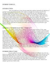
HYBRID VEHICLE:<br />
INTODUCTION:<br />
Have you pulled your car up to the gas pump lately and been shocked by the high price of<br />
gasoline? As the pump clicked past $20 or $30, maybe you thought about trading in that SUV for<br />
something that gets better mileage. Or maybe you are worried that your car is contributing to the<br />
greenhouse effect. Or maybe you just want to have the coolest car on the block. Currently, there is a<br />
solution for all this problems; it's the hybrid electric vehicle. The vehicle is lighter and roomier than a<br />
purely electric vehicle, because there is less need to carry as many heavy batteries. The internal<br />
combustion engine in hybrid-electric is much smaller and lighter and more efficient than the engine in a<br />
conventional vehicle. In fact, most automobile manufacturers have announced plans to manufacture<br />
their own hybrid versions. How does a hybrid car work? What goes on under the hood to give you 20 or<br />
30 more miles per gallon than the standard automobile? And does it pollute less just because it gets<br />
better gas mileage.<br />
WHAT IS A "HYBRID ELECTRIC VEHICLE"?<br />
Any vehicle is hybrid when it combines two or more sources of power. In fact, many<br />
people have probably owned a hybrid vehicle at some point. For example, a mo-ped (a motorized pedal<br />
bike) is a type of hybrid because it combines the power of a gasoline engine with the pedal power of its<br />
rider. Hybrid electric vehicles are all around us. Most of the locomotives we see pulling trains are dieselelectric<br />
hybrids. Cities like Seattle have diesel-electric buses -- these can draw electric power from<br />
overhead wires or run on diesel when they are away from the wires. Giant mining trucks are often<br />
diesel-electric hybrids. Submarines are also hybrid vehicles -- some are nuclear-electric and some are<br />
diesel-electric. Any vehicle that combines two or more sources of power that can directly or indirectly<br />
provide propulsion power is a hybrid. The most commonly used hybrid is gasoline-electric hybrid car<br />
which is just a cross between a gasoline-powered car and an electric car. A 'gasoline-electric hybrid car'<br />
or 'hybrid electric vehicle' is a vehicle which relies not only on batteries but also on an internal<br />
combustion engine which drives a generator to provide the electricity and may also drive a wheel. In<br />
hybrid electric vehicle the engine is the final source of the energy used to power the car. All electric cars<br />
use batteries charged by an external source, leading to the problem of range which is being solved in<br />
hybrid electric vehicle.<br />
HYBRID STRUCTURE:<br />
You can combine the two power sources found in a hybrid car in different ways. One way,<br />
known as a parallel hybrid, has a fuel tank, which supplies gasoline to the engine. But it also has a set of<br />
batteries that supplies power to an electric motor. Both the engine and the electric motor can turn the<br />
transmission at the same time, and the transmission then turns the wheels.We are all familiar with<br />
gasoline-powered cars, and most people have heard about or seen electric cars. A hybrid car is a<br />
combination of the two. A hybrid vehicle contains parts of both gasoline and electric vehicles in an<br />
attempt to get the best of both worlds.
The best way to understand the advantages of a hybrid vehicle is to think about a car traveling down a<br />
highway at the posted speed on level ground. In this case, the engine is doing three things:<br />
*It is overcoming rolling resistance in the drive train.<br />
*It is overcoming air resistance.<br />
*It is powering accessories like the alternator, the power steering pump and the air conditioner.The<br />
engine might need to produce no more than 10 or 20 horsepower (HP) to carry this load. The reason why<br />
cars have 100- or 200-horsepower engines to is handle acceleration from a standing stop, as well as for<br />
passing and hill climbing. We only use the maximum HP rating for 1% of our driving time. The rest of the<br />
time, we are carrying around the weight and the friction of the much larger engine, which wastes a lot of<br />
energy.<br />
In a traditional hybrid vehicle, you have a complete electric car. It includes an electric motor to provide<br />
all of the power to the wheels, as well as batteries to supply the motor with electricity. Then you have a<br />
completely separate gasoline engine powering a generator. The engine is very small -- perhaps 10 to 20<br />
horsepower -- and it is designed to run at just one speed for maximum efficiency. The purpose of this small,<br />
efficient engine is to provide enough power for the car at its cruising speed. During times of acceleration, the<br />
batteries provide the extra power necessary. When the car is decelerating or standing still, the batteries<br />
recharge. This sort of hybrid car is essentially an electric car with a built-in recharge for longer range. The<br />
advantage is that the small, efficient gasoline engine gets great mileage.<br />
HYBRID CAR:<br />
The only problem with a traditional hybrid car is the weight. The car has to carry the<br />
weight of the electric motor, the generator, the gasoline engine and the batteries. You<br />
don't need as many batteries as a pure electric car, so that saves some weight, but a fullsize<br />
electric motor plus a 10-kilowatt generator can weigh several hundred pounds
Increasing microprocessor speed<br />
The microprocessor inside the common computer is a small<br />
programmable device comprised of smaller devices called transistors. These<br />
transistors are circuits that switch electric signals from ‘on’ to ‘off’ and vice versa,<br />
incorporating a technology called the complementary metal-oxide semiconductor<br />
(CMOS). In modern microprocessors, the switching speed of transistors has been<br />
steadily increasing. However, overall microprocessor speeds have been held back by<br />
the quality of connections between transistors, limited by extant technology. To<br />
improve this, optical solutions have been suggested, where signals between<br />
transistors are not transferred through a circuit but by shining a laser between<br />
them. If implemented, this technique would increase microprocessor speeds. To<br />
make this happen, silicon, the main material in the CMOS industry, must work as a<br />
laser. When light of a particular frequency (colour) is shined on it, it must amplify<br />
the light’s power and then transmit it to nearby circuits. By 2006, hybrid silicon<br />
lasers were developed to do just this, but the technology has not become<br />
ubiquitous due to integration challenges and high costs. A recent paper published in<br />
Nature Photonics proposes a way out. Instead of silicon, researchers from the Paul<br />
Scherer Institute (PSI) and ETH, both Swiss, and Politecnico di Milano, Italy, have<br />
demonstrated that the element germanium (Gr) can be made to lase costeffectively<br />
and with fewer resources by stretching it a little. A slight tension is<br />
created in germanium by the way it is evaporated on silicon and the silicon is<br />
straightened. The tension induces a strain in germanium, and the researchers<br />
exploited this to create thin, strained layers of germanium on silicon strips. Next,<br />
they chipped away the sides of the germanium layer along the length, rendering the<br />
layer ‘I’-shaped, whose middle section was a narrow constricted bridge, called a<br />
micro bridge. Because strain is inversely proportional to the cross-sectional area, it<br />
is higher in the micro bridge than at the ends. The electrons in Gr atoms in the<br />
micro bridge must jump from a higher energy to a lower energy. When this jump<br />
happens, energy is released in the form of photons. This results in lasing. There is a<br />
compulsion to keep the micro bridge in a strained state to allow even the energydeficient<br />
electrons to jump. By stretching the micro bridge by 3.1 per cent, the team<br />
found that the material deforms enough to allow even the electrons that fall short<br />
by 3.2 x 10 joules to jump. In this stretched state, the micro bridge emits around 25<br />
times more photons than when in a relaxed state, which is “enough to build lasers,”<br />
says Richard Geiger, a doctoral student at PSI and part of the team.
Nanotechnology aids in cooling electrons without<br />
external sources<br />
A team of researchers has discovered a way to cool electrons to -<br />
228 C without external means and at room temperature, an advancement<br />
that could enable electronic devices to function with very little energy. The<br />
process involves passing electrons through a quantum well to cool them<br />
and keep them from heating.<br />
The team details its research in “Energy-filtered cold electron transport at room<br />
temperature,” which is published in Nature Communications on Wednesday, Sept.<br />
10.“We are the first to effectively cool electrons at room temperature. Researchers have<br />
done electron cooling before, but only when the entire device is immersed into an<br />
extremely cold cooling bath,” said Seong Jin Koh, an associate professor at UT Arlington<br />
in the Materials Science & Engineering Department, who has led the research.<br />
“Obtaining cold electrons at room temperature has enormous technical benefits. For<br />
example, the requirement of using liquid helium or liquid nitrogen for cooling electrons<br />
in various electron systems can be lifted.”<br />
Electrons are thermally excited even at room temperature, which is a natural<br />
phenomenon. If that electron excitation could be suppressed, then the temperature of<br />
those electrons could be effectively lowered without external cooling, Koh said. The<br />
team used a nanoscale structure—which consists of a sequential array of a source<br />
electrode, a quantum well, a tunneling barrier, a quantum dot, another tunneling<br />
barrier, and a drain electrode—to suppress electron excitation and to make electrons<br />
cold.
Cold electrons promise a new type of transistor that can operate at<br />
extremely low-energy consumption. “Implementing our findings to fabricating<br />
energy-efficient transistors is currently under way,” Koh added.<br />
Khosrow Behbehani, dean of the UT Arlington College of Engineering, said<br />
this research is representative of the University’s role in fostering<br />
innovations that benefit the society, such as creating energy-efficient green<br />
technologies for current and future generations.<br />
“Dr. Koh and his research team are developing real-world solutions to a<br />
critical global challenge of utilizing the energy efficiently and developing<br />
energy-efficient electronic technology that will benefit us all every day,”<br />
Behbehani said. “We applaud Dr. Koh for the results of this research and<br />
look forward to future innovations he will lead.”<br />
Usha Varshney, program director in the National Science Foundation’s<br />
Directorate for Engineering, which funded the research, said the research<br />
findings could be vast.<br />
“When implemented in transistors, these research findings could potentially<br />
reduce energy consumption of electronic devices by more than 10 times<br />
compared to the present technology,” Varshney said. “Personal electronic<br />
devices such as smart phones, iPads, etc., can last much longer before<br />
recharging.”<br />
In addition to potential commercial applications, there are many military uses<br />
for the technology. Batteries weigh a lot, and less power consumption<br />
means reducing the battery weight of electronic equipment that soldiers are<br />
carrying, which will enhance their combat capability. Other potential military<br />
applications include electronics for remote sensors, unmanned aerial<br />
vehicles and high-capacity computing in remote operations.<br />
Future research could include identifying key elements that will allow<br />
electrons to be cooled even further. The most important challenge of this<br />
future research is to keep the electron from gaining energy as it travels<br />
across device components. This would require research into how energygaining<br />
pathways could be effectively blocked.
World Record Solar Cell with 44.7% Efficiency<br />
The Fraunhofer Institute for Solar Energy Systems ISE, Soitec, CEA-Leti and the Helmholtz<br />
Center Berlin jointly announced today having achieved a new world record for the conversion of<br />
sunlight into electricity using a new solar cell structure with four solar subcells. Surpassing<br />
competition after only over three years of research, and entering the roadmap at world class level, a<br />
new record efficiency of 44.7% was measured at a concentration of 297 suns. This indicates that<br />
44.7% of the solar spectrum's energy, from ultraviolet through to the infrared, is converted into<br />
electrical energy. This is a major step towards reducing further the costs of solar electricity and<br />
continues to pave the way to the 50% efficiency roadmap.<br />
Back in May 2013, the German-French team of Fraunhofer ISE, Soitec, CEA-Leti and the<br />
Helmholtz Center Berlin had already announced a solar cell with 43.6% efficiency. Building on this<br />
result, further intensive research work and optimization steps led to the present efficiency of 44.7%.<br />
These solar cells are used in concentrator photovoltaic (CPV), a technology which achieves more than<br />
twice the efficiency of conventional PV power plants in sun-rich locations. The terrestrial use of socalled<br />
III-V multi-junction solar cells, which originally came from space technology, has prevailed to<br />
realize highest efficiencies for the conversion of sunlight to electricity. In this multi-junction solar cell,<br />
several cells made out of different III-V semiconductor materials are stacked on top of each other. The<br />
single subcells absorb different wavelength ranges of the solar spectrum.<br />
“We are incredibly proud of our team which has been working now for three years on this f<br />
our-junction solar cell,” says Frank Dimroth, Department Head and Project Leader in charge of this<br />
development work at Fraunhofer ISE. “This four-junction solar cell contains our collected expertise in<br />
this area over many years. Besides improved materials and optimization of the structure, a new<br />
procedure called wafer bonding plays a central role. With this technology, we are able to connect two<br />
semiconductor crystals, which otherwise cannot be grown on top of each other with high crystal<br />
quality. In this way we can produce the optimal semiconductor combination to create the highest<br />
efficiency solar cells.”<br />
“This world record increasing our efficiency level by more than 1 point in less than 4 months<br />
demonstrates the extreme potential of our four-junction solar cell design which relies on Soitec bonding<br />
techniques and expertise,” says André-Jacques Auberton-Hervé, Soitec’s Chairman and CEO. “It<br />
confirms the acceleration of the roadmap towards higher efficiencies which represents a key<br />
contributor to competitiveness of our own CPV systems. We are very proud of this achievement, a<br />
demonstration of a very successful collaboration.”
“This new record value reinforces the credibility of the direct semiconductor<br />
bonding approaches that is developed in the frame of our collaboration with<br />
Soitec and Fraunhofer ISE. We are very proud of this new result, confirming the<br />
broad path that exists in solar technologies for advanced III-V semiconductor<br />
processing,” said Leti CEO Laurent Malier.<br />
Concentrator modules are produced by Soitec (started in 2005 under the name<br />
Concentrix Solar, a spin-off of Fraunhofer ISE). This particularly efficient<br />
technology is employed in solar power plants located in sun-rich regions with a<br />
high percentage of direct radiation. Presently Soitec has CPV installations in 18<br />
different countries including Italy, France, South Africa and California.<br />
IV-characteristic for the current best four-junction solar cell under AM1.5d<br />
ASTM G173-03 spectrum at a concentration of 297 suns. The measurements<br />
were carried out at the Fraunhofer ISE CalLab. ©Fraunhofer ISE<br />
External Quantum Efficiency of the four-junction solar cell. The measurement<br />
was performed at the Fraunhofer ISE CalLab. ©Fraunhofer ISE
First water-based nuclear battery can be used to<br />
generate electrical energy<br />
From cell phones to cars and flashlights, batteries play an<br />
important role in everyday life. Scientists and technology companies<br />
constantly are seeking ways to improve battery life and efficiency. Now,<br />
for the first time using a water-based solution, researchers at the<br />
University of Missouri have created a long-lasting and more efficient<br />
nuclear battery that could be used for many applications such as a<br />
reliable energy source in automobiles and also in complicated<br />
applications such as space flight.<br />
“Betavoltaics, a battery technology that generates power<br />
from radiation, has been studied as an energy source since the<br />
1950s,” said Jae W. Kwon, an associate professor of electrical and<br />
computer engineering and nuclear engineering in the College of<br />
Engineering at MU. “Controlled nuclear technologies are not inherently<br />
dangerous. We already have many commercial uses of nuclear<br />
technologies in our lives including fire detectors in bedrooms and<br />
emergency exit signs in buildings.”<br />
The battery uses a radioactive isotope called strontium-90<br />
that boosts electrochemical energy in a water-based solution. A<br />
nanostructured titanium dioxide electrode (the common element found<br />
in sunscreens and UV blockers) with a platinum coating collects and<br />
effectively converts energy into electrons.<br />
“Water acts as a buffer and surface Plasmon’s created in the device<br />
turned out to be very useful in increasing its efficiency,” Kwon said.<br />
“The ionic solution is not easily frozen at very low temperatures and<br />
could work in a wide variety of applications including car batteries and,<br />
if packaged properly, perhaps spacecraft.” The research, “Plasmonassisted<br />
radiolytic energy conversion in aqueous solutions,” was<br />
conducted by Kwon’s research group at MU, and was published in<br />
Nature.
Improving the efficiency of Solar panels<br />
"Rows of aluminium studs help solar panels extract more energy from sunlight than<br />
those with flat surfaces." This picture shows a solar panel with rows of aluminium studs<br />
and large electrical connections. The studs have been enlarged here but would normally<br />
be so small that they are invisible to the naked eye. (source:Imperial college<br />
London/Nicholas Hylton)<br />
Light scattering was promoted in the visible part of sunlight's spectrum<br />
At the heart of the blooming solar power industry is the semiconductor material, like<br />
silicon or gallium arsenide, which absorbs sunlight and forms the basis of solar panels. It<br />
converts electro<strong>mag</strong>netic energy in the form of sunlight to electrical energy. Now,<br />
researchers from London have demonstrated a technique to increase the amount of<br />
electrical current produced by a solar panel simply by augmenting its light-facing surface<br />
with aluminium nanostructures. When photons, particles of light, are absorbed by the<br />
semiconductor, they knock out electrons, which are passed through a circuit and then to<br />
a battery for storage as electricity. However, scientists now want to find ways of<br />
Increasing the absorption of light in thin layers of semiconductors, so that solar panels<br />
can be made using less raw-material and at a lower cost. Recent research from the<br />
Imperial College, London (ICL), has demonstrated one way to increase the electrical<br />
current produced by devices in the lab by 22 per cent. By studding the light-receiving<br />
surface of gallium-arsenide (Ga-As) devices with aluminium nanocylinders, like the ridges<br />
on Lego blocks, the researchers were able to promote the scattering of light in the visible<br />
part of the spectrum, which dominates the energy in sunlight. The scattered light then<br />
travels a longer path inside the semiconductor, meaning that more photons can be<br />
absorbed and converted into current. It is important that the metal nanocylinders do not<br />
absorb
The light themselves, as that would prevent it from<br />
reaching the panel. “The advantage of aluminium structures is that<br />
their absorption occurs in the ultraviolet part of the spectrum. That<br />
means that the absorption losses are limited to the ultraviolet and<br />
scattering from the aluminium particle dominates in both the visible<br />
and near infrared,” said Dr. Nicholas Hylton, a Research Associate at<br />
the Blackett Laboratory, ICL, in an email.<br />
Dr. Hylton was lead author of the research group’s paper,<br />
published in Scientific Reports on October 18. This isn’t the first time<br />
such nanostructures have been deployed to enhance the performance<br />
of solar panels. Earlier, silver and gold nanoparticles have been used<br />
because they improved the performance of the devices in the nearinfrared<br />
part of the electro<strong>mag</strong>netic spectrum. “We were able to<br />
demonstrate that gold and silver scatter light in the near infrared part<br />
of the spectrum but absorb visible light strongly,” Dr. Hylton<br />
wrote.The significance of Dr.Hylton’s work lies in demonstrating<br />
aluminium’s better performance over silver and gold nanostructures.<br />
For one, aluminium is more abundant and less costly than silver and<br />
gold. For another, the 22 per cent spike that aluminium provides, as<br />
their paper notes, makes thinner-film solar panels technically feasible<br />
without “compromising powerconversion efficiencies, thus reducing<br />
material consumption.”Higher efficiency devices could play a<br />
significant role in realising energy goals even in India, making them<br />
more cost-effective. Already, according to industry trackers, the price<br />
of solar power in India has come from Rs. 18/kWh in 2011 to Rs.<br />
7/kWh in 2013, while the price of thermal power is pushing Rs.<br />
4/kWh with subsidies.
Innovations in FACTS Technology<br />
In series compensation, a capacitor is used to compensate for the lines impedance, thus<br />
the line is "virtually" shortened and the transmission angle decreased for system stability improvement.<br />
However, during transient conditions, the short-circuit currents cause high voltages across the capacitor,<br />
which must be limited to specified values. In the past, this limitation was accomplished by arresters (MOV)<br />
in combination with a spark gap. An AC-fault current flowing through a MOV always leads to a high energy<br />
dissipation of the MOV.The MOV heats up heavily. Due to an upper temperature limit the MOV must cool<br />
down before the next current stress can be absorbed. Cooling down requires a large amount of time, time<br />
constants of several hours are known. During this time, the series compensation must be taken out of<br />
service (bypass-breaker closed) and consequently the power transfer on the related line needs to be<br />
reduced dependent on the degree of compensation. Both the (mechanical) gap function and the MOV can<br />
now be replaced by an innovative solution with special high power light-triggered thyristors. These<br />
thyristors are designed and tested for a 110 kA peak current capability and they have a very fast coolingdown<br />
time. Using this new technology, significant cost savings after system faults can be achieved. The<br />
principle of the TPSC and the cost savings for each fault on one of the 3 lines at the 500 kV TPSC installation<br />
at Vincent Substation, USA. In case of faults nearby the substations all 3 lines are involved in the fault<br />
strategy. Then the savings sum up to 270.000 US$ per event to Substation to Line<br />
Benefits of 90.000 US$ per event on 1 line due to faster available TPSC<br />
e.g. reduction from 1200 MW to 600 MW with FSC/MOV * * 25 US$/MWh x 600 MW x 6 hrs<br />
Increasing generation in high load density networks on one hand and interconnections<br />
among the systems on the other, increases the short-circuit power. If the short-circuit current rating of the<br />
equipment in the system is exceeded, the equipment must be upgraded or replaced, which is a very costand<br />
time-intensive procedure. Short-circuit current limitation offers clear benefits in such cases. Limitation<br />
by passive elements, e.g. reactors, is a well known practice, however it reduces the system stability and<br />
there is impact on the load-flow. By combining the TPSC with an external reactor, whose design is<br />
determined by the allowed short circuit current level, this device can also be used very effectively as a<br />
short-circuit current limiter (SCCL). This new device operates with zero impedance in steady-state<br />
conditions, and in case of a short-circuit it is switched within a few ms to the limiting-reactor impedance. In<br />
comparison with the TPSC site view it can be seen, that the TPSC is just complemented by an additional<br />
reactor for the current limitation. By means of control add-on functions, both TPSC and SCCL can also be<br />
applied for power oscillation damping and for mitigation of sub synchronous resonances (SSR). In<br />
conclusion, with the FACTS based TPSC and SCCL, an innovative break-through in transmission technology<br />
for high-voltage systems has been achieved.
MEMRISTOR TECHNOLOGY FROM HP<br />
Blocks and Files HP has warned El Reg not to get its hopes up too high<br />
after the tech titan's CTO Martin Fink suggested Store Serve arrays could be packed with 100TB<br />
Memristor drives come 2018. In five years, according to Fink, DRAM and NAND scaling will hit a<br />
wall, limiting the maximum capacity of the technologies: process shrinks will come to a shuddering<br />
halt when the memories' reliability drops off a cliff as a side effect of reducing the size of<br />
electronics on the silicon dies. The HP answer to this scaling wall is Memristor, its flavour of<br />
resistive RAM technology that is supposed to have DRAM-like speed and better-than-NAND<br />
storage density. Fink claimed at an HP Discover event in Las Vegas that Memristor devices will be<br />
ready by the time flash NAND hits its limit in five years. He also showed off a Memristor wafer,<br />
adding that it could have a 1.5PB capacity by the end of the decade.<br />
.<br />
The HP Labs boss also said that, by 2018, we could pop 100TB Memristor drives into Store Serve<br />
arrays. Today a 3PAR Store Serve 7450 enclosure can have 240 solid-state drives, supporting a<br />
maximum raw capacity of 96TB raw capacity using 400GB SSDs. Now i<strong>mag</strong>ine 240 100TB Memristor<br />
drives in such a box: that's 24,000TB or 24PB. Fink spoke about the tech in June, but this week a HP<br />
spokesperson clarified As with many other ground-breaking technologies being developed at HP Labs,<br />
HP has not yet committed to a specific product roadmap for Memristor-based products. HP does have<br />
internal milestones that are subject to change, depending on shifting market, technology and business<br />
conditions. On day one, Fink said in Las Vegas, Memristor density will be higher and speed faster than<br />
flash, but it won't be as fast as DRAM. Over time its access latency will decrease, we're assured.<br />
Memristor cells could be multi-layer, with two-bit-per-cell and three-bit-per-cell versions<br />
achievable,added Fink. He also claimed Memristor layers could be stacked, with four layers achievable<br />
and six possible. We assumed Memristor drives would be introduced by HP before 2018; now the<br />
company's saying the plan is still up in the air. So, there is still no specific product roadmap but HP’s<br />
CTO talked confidently of HP popping 100TB Memristor drives into StoreServ arrays in five years. He<br />
also said Memristor could be a universal memory, replacing both DRAM and flash and hinted at<br />
specialised Moonshot cartridges, possibly using Memristor memory instead of DRAM, linked by terabitclass<br />
photonic connects to Memristor Store Serv arrays.
New circuit design functions<br />
At temperatures >> 650 0 F<br />
Engineering researchers at the University of Arkansas have<br />
designed integrated circuits that can survive at temperatures greater than 350 C—or roughly<br />
660 F. Their work, funded by the National Science Foundation, will improve the functioning<br />
of processors, drivers, controllers and other analog and digital circuits used in power<br />
electronics, automobiles and aerospace equipment—all of which must perform at high and<br />
often extreme temperatures. “This ruggedness allows these circuits to be placed in locations<br />
where standard silicon-based parts can’t survive,” said Alan Mantooth, Distinguished<br />
Professor. “The circuit blocks we designed contributed to superior performance of signal<br />
processing, controllers and driver circuitry. We are extremely excited about the results so far.<br />
The research is critical because one-third of all power<br />
produced in the United States passes through some kind of power electronic converter or<br />
motor drive before it reaches the end user. Circuits developed by the University of Arkansas<br />
team will enable tight integration of control in the tough environmental conditions these<br />
applications demand. They will also improve electrical efficiency while simultaneously<br />
reducing the overall size and complexity of these systems.The researchers worked with<br />
silicon carbide, a semiconducting material that is more rugged than conventional materials<br />
used in electronics. Silicon carbide is able to withstand extremely high voltage and is a good<br />
thermal conductor, meaning it can operate at high temperatures without requiring extra<br />
equipment to remove heat. The research team, led by Mantooth and Jia Di, professor of<br />
computer engineering, achieved the higher performance by combining silicon carbide with<br />
wide temperature design techniques.<br />
In the world of power electronics and integrated circuits,<br />
their work represents the first implementation of a number of fundamental analog, digital and<br />
mixed-signal blocks, such as a phase-locked loop using a complimentary-style silicon carbide<br />
technology. A phase-locked loop, or PLL, is a control system that generates an output signal<br />
whose phase is related to the phase of an input signal. Such a function is critical in a number<br />
of circuit applications such as signal synchronization, frequency synthesis, and modulation<br />
and demodulation schemes
The research was part of the National Science<br />
Foundation’s Building Innovation Capacity program, which is designed to<br />
partner university and industry research to build intellectual collaborations so<br />
that innovations flow from ideas to solid research results, company prototypes<br />
and products. The University of Arkansas and two Fayetteville technology<br />
firms, Ozark Integrated Circuits and Arkansas Power Electronics International,<br />
form the basis for this innovation ecosystem. Raytheon is also a key partner.<br />
Ozark Integrated Circuits is commercializing the circuit technology. Arkansas<br />
Power Electronics International focuses on using the circuits in power<br />
applications. The research funding was awarded to Arkansas Circuit Design<br />
Center, which is comprised of two laboratories, one directed by Mantooth and<br />
one by Di. The Arkansas Circuit Design Center supports the mission of the<br />
University of Arkansas’ National Center for Reliable Electric Power<br />
Transmission, which is funded as part of the federal government’s focus on<br />
research and development on smart grid and renewable technologies.<br />
The centre is one of only a few university-based<br />
research centres investigating electronic systems to make the nation’s power<br />
grid more reliable and efficient. The U.S. Department of Energy has funded the<br />
centre since 2005 because of the university’s research expertise in advanced<br />
power electronics and long term investigation of silicon carbide.<br />
Mantooth is executive director of the center.Arkansas<br />
Power Electronics International specializes in advanced, high-performance<br />
electronics for a variety of customers and applications, including the defense,<br />
aerospace and hybrid/electric vehicle markets. Ozark Integrated Circuits is a<br />
semiconductor company that develops integrated circuits for remote sensing<br />
and actuation under extreme environmental conditions. Mantooth is holder of<br />
the Twenty-First Century Chair in Mixed-Signal Integrated Circuit Design and<br />
Computer-Aided Design in the College of Engineering.<br />
-Ambarish M S<br />
(Pre Final Year EEE A)
Cambridge team identifies high temperature superconductors<br />
Researchers from the University of Cambridge say they<br />
have made a big step in developing new high temperature superconducting materials<br />
which could be used in lossless electrical grids, next-generation supercomputers and<br />
levitating trains. The researchers have found that ripples of electrons, known as<br />
charge density waves or charge order, create twisted ‘pockets’ of electrons in these<br />
materials, from which superconductivity emerges. The results are published in the<br />
June 15th issue of the journal Nature. Low-temperature, or conventional,<br />
superconductors were first identified in the early 20th century, but they need to be<br />
cooled close to absolute zero (zero degrees on the Kelvin scale, or -273 o C) before<br />
they start to display superconductivity. So-called high-temperature superconductors<br />
however, can display the same properties at temperatures up to 138 Kelvin (-135 0 C),<br />
making them much more suitable for practical applications. However, the process of<br />
discovering new high-temperature superconductors could be best described as<br />
random.<br />
“One of the problems with high-temperature superconductors<br />
is that we don’t know how to find new ones, because we don’t actually know what<br />
the ingredients are that are responsible for creating high-temperature<br />
superconductivity in the first place,” said Dr Suchitra Sebastian of the Cavendish<br />
Laboratory, lead author of the paper. “We know there’s some sort of glue which<br />
causes the electrons to pair up, but we don’t know what that glue is,” said Sebastian.<br />
In a superconductor, as in any electronic device, current is carried via the charge on<br />
an electron. What is different about superconductors is that the electrons travel in<br />
tightly bound pairs. When travelling on their own, electrons tend to bump into each<br />
other, resulting in a loss of energy. But when paired up, the electrons move smoothly<br />
through a superconductor’s structure, which is why superconductors can carry<br />
current with no resistance. Key to conventional superconductors are the interactions<br />
of electrons with the lattice structure of the material. These interactions generate a<br />
type of ‘glue’ which holds the electrons together.
The strength of the glue is directly related to the strength of the<br />
superconductor, and when the superconductor is exposed to an increase in temperature<br />
or <strong>mag</strong>netic field strength, the glue is weakened, the electron pairs break apart and<br />
superconductivity is Lost “We’re trying to understand what sorts of interactions were<br />
happening in the material before the electrons paired up, because one of those<br />
interactions must be responsible for creating the glue,” said Dr Sebastian.<br />
“Once the electrons are already paired up, it’s hard to know what made<br />
them pair up. But if we can break the pairs apart, then we can see what the electrons are<br />
doing and hopefully understand where the superconductivity came from.”<br />
Superconductivity tends to override other properties. For example, if in its normal state<br />
a superconductor was a <strong>mag</strong>net, suppressing that <strong>mag</strong>netism has been found to result in<br />
superconductivity. “So by determining the normal state of a superconductor, it would<br />
make the process of identifying new ones much less random, as we’d know what sorts<br />
of materials to be looking for in the first place,” said Dr Sebastian. Previous attempts to<br />
determine the origins of superconductivity by determining the normal state have used<br />
temperature instead of <strong>mag</strong>netic field to break the electron pairs apart, which has led to<br />
inconclusive results. “By identifying other materials which have similar properties,<br />
hopefully it will help us find new superconductors at higher and higher temperatures,<br />
even perhaps materials which are superconductors at room temperature, which would<br />
open up a huge range of applications,” said Dr Sebastian
Non<br />
Technical<br />
Articles
How Engineers Do It:<br />
-Engineers do it with precision.<br />
-Electrical engineers are shocked when they do it.<br />
-Electrical engineers do it on an impulse.<br />
-Electrical engineers do it with large capacities.<br />
-Electrical engineers do it with more frequency and less resistance.<br />
-Electrical engineers do it with more power and at higher frequency.<br />
Technical Jokes:<br />
1. What did the light bulb say to the generator? "I really get a charge out<br />
of you!"<br />
2. How do you pick out a dead battery from a pile of good ones? “ It's<br />
got no spark!”<br />
3. A man with a hearing problem walked into a power plant for a tour. He<br />
arrived late and had to join the rest of the group already on the tour. The<br />
man was reviewing what he had just told the group. He told the group that<br />
they wouldn't move on untill they answered this one question: "What is<br />
the unit of power equal to one joule per second called?" The man with the<br />
hearing problem hadn't heard the question very well, so he raised his hand<br />
and asked "What?"<br />
4. Why do transformers hum? “They don't know the words.”<br />
5. What did the light bulb say to the electric generator? "You spark up<br />
my life!"<br />
6. What did the baby light bulb say to the mommy light bulb? "I love<br />
you watts and watts!"<br />
7. Why was the free electron so sad? “It had nothing to be positive<br />
about!”<br />
8. What did Godzilla say when he ate the nuclear power plant?<br />
"Shocking!"<br />
9. Why did the lights go out? “ Because they liked each other!”<br />
10. Two atoms were walking down the street one day, when one of them<br />
exclaimed, "Oh, no I've lost an electron!" "Are you sure?" the other one<br />
asked. "Yes," replied the first one, "I'm positive."
My Inner Voice to Raise Our Voice<br />
It is about my experience which I had on August 16, the day after our<br />
Independence Day. After hearing the P.M’s Independence Day speech somehow I came to<br />
know about “MY GOV”, a social networking and citizen engagement platform, which<br />
was launched by the government of India. Its aim is to reduce the wide gap between the<br />
electorate and the executive (Government) after being elected. It allows the users to<br />
discuss and contribute to various government projects and plans. The platform is divided<br />
into various groups. The group’s objective is to bring positive changes in the relevant<br />
areas with people’s participation. The users are provided with two domains ‘DO’ and<br />
‘Discuss’. The ‘Do’ section includes both online and on-ground tasks, one can assign<br />
themselves. The ‘Discuss’ section may be used for discussing important issues which<br />
affect the nation.<br />
After creating my account in this website, I wished to spread information<br />
about this new platform to my friends. So I shared a link about this on the omnipresent<br />
social network ‘Facebook’ which is the second home for most of the people in our<br />
generation. I also shared that link with various groups and chats to which I belong in<br />
facebook and was hoping to get some positive responses from my friends. But<br />
unfortunately all my efforts went in vain as no one responded to it except 2 people who<br />
liked the share,(maybe) just for namesake. When topics like cricket, movies and other<br />
entertainment stuffs get huge responses on social media, fruitful ones like the “thinking<br />
for nation and society” topic don’t quite get them. Every one of us are spending our time<br />
in discussing about movie box offices, their flaws and recent performances of our cricket<br />
team for a whole day, but no one is ready to spend even half an hour thinking about their<br />
motherland. For an example, in that website one of the topics is ‘clean India’ which deals<br />
about the cleanliness of our country. Most of us commonly say “look at the other foreign<br />
countries and our nation, see how neat and clean they are and how unclean we are”. No<br />
one will spit or throw garbage inside our home but when we are out in the streets or<br />
public places, polluting our ‘homeland’ without any guiltiness becomes the natural habit.<br />
It is because only our homes are taught to be kept clean, not our nation
To some extent it even teaches, “To keep yourself clean<br />
you can pollute anyone and anything, there is nothing wrong in it”.<br />
Students in our country do not want to fail or get low marks in exams<br />
mostly because of the pressure given by external factors like friends who<br />
would be the first in our comparison, parents who may worry about<br />
getting low marks more than us and society which will tare you apart<br />
when you fail. But unfortunately none of these factors ever create any<br />
pressure when it comes to general issue. It is the place where our<br />
Individualism diminishes our patriotism.<br />
For these many days we have been accusing our<br />
government’s inability to develop our nation. But somehow now we have<br />
got a chance to contribute to the changes, which we desire. So please take<br />
active participation in this site and do it as your mandatory duty for the<br />
nation. The success of this article lies in how it spreads across people and<br />
creates a positive impact in their mind. By creating an impact it shouldn’t<br />
get stagnated in the form of ideas. It should be transformed as positive<br />
actions and practices being performed by every one of us. Now we are<br />
living peacefully in our country without facing any life threatening<br />
problems. But the importance of our nation will be exposed only if we<br />
face awful circumstances which are being faced by countries like<br />
Palestine, Syria, Iraq and our neighbor Srilanka, but hopefully do not. So<br />
our patriotism shouldn’t be contented only with changing display picture<br />
and singing national anthem on 15 th of august. We should go far beyond<br />
these simple things and try to serve our birthplace in any way which we<br />
are capable of…<br />
Long live India…<br />
V.Kannan<br />
Pre-Final Year EEE A
DAHIBATH<br />
(THAYIR SADAM OR CURD RICE)<br />
Thayir sadam presides over the lunches and dinners of brahminical homes for<br />
ages. Thayir sadam is identified with Brahmins so much so that brahmincal youths often become the<br />
butt end of wit by being referred to endearingly as ‘Thayir sadam’.In the south, no lunch or dinner is<br />
complete without Thayir sadam at the end. While we travel to the remotest corners of the globe,<br />
when we sight even half a plateful Thayir sadam, we feel as excited, as Archimedes was, when he<br />
shouted “Eureka, Eureka”.<br />
Thayir sadam essentially consists of cooked rice mixed with curd and salted a little to appeal to our<br />
palate. Many dress it up with finely cut pieces of green chillies, ginger (or rather its dried variety<br />
sukku), slightly fried mustard. During travel, to enhance its shelf life more and to prevent it from<br />
turning sour, a little milk is also added. In those days, for train journeys, a dubba full of molagapodi<br />
spread idlies, packed Thayir sadam ensured to be free from becoming sour, a kooja full of hot coffee<br />
supplemented by a flask full and tickets (card tickets and no E ticket) in that order were essential<br />
requisites.<br />
Simplicity thy name is Thayir sadam. When we have butterflies in our stomach or when we have<br />
absolutely no appetite, Thayir sadam would act as a palliative. Don’t go to bed, without having at<br />
least a mouthful of Thayir sadam, our anxious grandmothers would admonish us. If one cannot<br />
afford a three course lunch or dinner, a mouthful of Thayir sadam, two times a day, would sustain<br />
us.<br />
By nature, Thayir sadam is gregarious. It cannot suffer loneliness. Pickles, particularly aavakkai,<br />
mavadu or vadu mangai ( kaduku mangai)and Thayir sadam are made for each other. A spoonful of<br />
manga kari ( raw finely cut mangoes, mixed with salt and chilly powder), when fresh (not more<br />
than 2 days old) adds Thayir sadam an extra taste incomparable to any sensuous pleasure in the<br />
world. Thayir sadam also gets along well with narthangai, nellikkai and limbu. Those whose<br />
Cholesterol level is normal can also go for fried moremilagai, chundakkai and marthankali or<br />
thamaraikizhanku. I know people who take Thayir sadam along with sediments of rasam. Light<br />
heartedly, one could say that if Thayir sadam had been available during lunch at Lords, a Srikant<br />
would have crossed the boundaries more often or a Venkat Raghavan turned his off- spinners a little<br />
more sharp at Oval. It is quality Thayir sadam that has added to the assertiveness if not arrogance,<br />
of some of the cricket officials. During marriage eve dinners, when the contractors provide North<br />
Indian or Western dishes along with chat and Chinese items, Thayir sadam finds a pride of place<br />
among strangers. Would any one need a proof of its popularity? The solid version of Thayir sadam is<br />
reverentially addressed as ‘daddhi annam’ by the Vaishnavaites whereas its diluted form bears the<br />
name baghala bath’. A well dressed thayhir sadam charm us and lead us like the Pied Piper of<br />
Hamelin. Thayir sadam is also distributed as prasadam in Vishnu temples. Once when we were at<br />
Govindapuram(nearKumbakonam) a littlelater than,Lunch hour and as lunch had been exhausted<br />
we were served Thayir sadam with lime pickles instead. What a Divine Grace! Gavasdkar’s glorious<br />
Century at Old Trafford, Jim Laker’s 19 for 90 again at Old Trafford, Maradona’s dribblings with the<br />
ball, all pale into insignificance before that Thayir sadam.
Those unfamiliar with their kitchen or young daughter-in –laws fresh<br />
from colleges, untrained by their mothers in culinary art, find solace and satiety in Thayir<br />
sadam. Even though an essential part of lunches and dinners or serving as a standard<br />
alone item, thayir sadam is asked to stand out from our breakfast tables. To have taken<br />
Thayir sadam for breakfast means one has committed an unforgivable sin and is beyond<br />
redemption. All the efforts in preparing Thayir sadam remain unappreciated. I could pack<br />
only Thayir sadam today in my child’s lunch box, a young mother would say with a tone<br />
full of sin. Her preparation of even Thayir sadam is a curse, a mother in law would<br />
lament about her daughter in law’s inadequacies. Ambi, modalla Thayir sadam panna<br />
padichukko, appuram adupu kitta wa, a senior cook would admonish the young recruit<br />
who struggles with stirring the sambar. North Indians take dahi aplenty without making<br />
Thayir sadam out of it. Even among communities in our own Kerala, other than Brahmins<br />
do not have much fancy for dahi bath. However, in Tamil Nadu, all communities<br />
comfortably settle for Thayir sadam. In western countries, Yoghurt, as curd is called,<br />
takes shape in different flavors and serves as a desert.<br />
In fact, some of the Airlines serve flavored yoghurt in cups. Thayir<br />
sadam has therapeutic value. Endowed with bacteria that fight the ones causing us<br />
diseases, Thayir sadam helps us in digestion, cleanses our colons and ensures smooth<br />
disposal of wastages from our system. A handful of Thayir sadam three times a day is<br />
equivalent to eight grandmas around us, an unmarried youth, surviving on Thayir sadam<br />
alone, in a remote corner in Europe, sings its glory. Though virtues galore, Thayir sadam<br />
suffers from a serious setback. One has to be free from Thayir sadam, when one is<br />
suffering from a high temperature or has a running nose. On such occasions, milagu<br />
rasam ( pepper rasam) is prescribed instead. If during their dating days, one of the duo<br />
indicates his/her preference for Thayir sadam, would run the risk of ruining the<br />
relationship. It is not merely IITs and other engineering colleges that have contributed<br />
towards the development of Silicon Valley. Thayir Sadam that sustained software<br />
engineers in Indian Soil, if not in San Francisco, has also contributed in equal measure in<br />
the mission. Like Intel Inside, if an indication that “Thayir Sadam Inside”, is available, that<br />
would announce to the world that best of operations is at hand.<br />
Dr.D.KalyanaKumar<br />
Dept.of EEE
NFC<br />
(Near FieldCommunication)<br />
As many knows about Bluetooth is a wireless technology to transmit<br />
data between devices over short range similar to that NFC is also a short range frequency wireless<br />
communication technology that enables to exchange data’s (Photos, videos etc…) between devices<br />
(such as smart phones, smart TV etc…)about a distance of 10 cm. It was founded in 2004 by sony ,<br />
nokia and Philips.<br />
Same as Bluetooth we can exchange our data’s between devices but the<br />
significant advantage of NFC is the shorter set up time. Instead of performing manual configurations<br />
to identify Bluetooth devices the connection between two NFC devices is established under (1/10<br />
second).Due to its short range it provides high security. And it also works if one device is not powered<br />
(eg: if a phone turned off). It can replace the use of credit cards to pay bills. And in some modern cars<br />
it can be used as mobile key to open doors.<br />
BY<br />
R.SUNIL<br />
(Pre Final year EEE”B”)
PARADOX<br />
The state of today’s in the world around us shows there is<br />
a huge amount of work to be done to set it right. But everyone complains there is less work<br />
opportunity. This statement is an example for anyone who wants to understand the meaning<br />
of Paradox. There are more examples to follow.<br />
The continuing trend of widening academia-industry gap,<br />
poses a threat to the development of society at large. In the existing scenario, it is a well<br />
known and commonly accepted fact, that there exists a huge gap between the industry and<br />
academia in our country. There could be some exceptions in case of IIT’s, NIT’s and few<br />
other reputed institutions, but the massive bunch of other self financing colleges hugely<br />
suffers on this gap. Consequently industries were not able to perform the recruitment<br />
fulfilling their intended requisites. Despite the fact India has one of the largest higher<br />
education systems in the world comprising of 700 plus universities, 35,000 plus colleges and<br />
numerous stand-alone technical/professional institutions with annual enrolment in excess of<br />
25 million students. Multiple surveys conducted by different organizations conclude that<br />
significant percentages of the students are not employable. But in all these surveys, that<br />
which is referred as industries includes IT and IT enabled service sectors and other few big<br />
core industries and MNC’s.<br />
Millions of students graduating from the engineering colleges are chasing towards<br />
thousands of jobs offered by IT and other MNC’s, Does it makes sense...<br />
More importantly the Micro small and medium scale<br />
enterprises (MSME) sector is not a part of this survey at all. MSMEs play a pivotal role in the<br />
overall industrial development of the country and they have been the significant contributor<br />
to the national income, with their huge involvement in country's industrial production,<br />
exports, etc. It is an interesting fact that the second largest sector in our country that provides<br />
employment to people next to agriculture is MSME. Thus, this sector has been regarded a<br />
priority status by both the Central and the State Governments. In spite of this MSME faces<br />
multiple issues for its day-day survival and growth. The human talents coming out of the<br />
educational institutions are of far reach for the MSME. On the other hand only a few<br />
percentage of the students graduating from engineering institutions lands up with a job. The<br />
above is a yet another example of a paradox situation. It is interesting to observe that the self<br />
financing engineering institutions and the MSME have an important stake in the development<br />
of each other.<br />
It makes sense to think out of box in establishing ones career in a meaningful manner.<br />
S.Lenin Prakash<br />
Asst.Prof. Dept of EEE
Testing the Basics<br />
1. Consider a two winding transformer, say 110/220 V. The<br />
primary is connected to the supply voltage and the secondary is<br />
connected to the load. Consider suddenly if the core disappears,<br />
what will happen?<br />
a.What happens to the secondary induced emf , terminal voltage ?<br />
b. Will it change? Justify your answer..<br />
c. What else will happen when the core is not there..<br />
Students shall think on it and email their detailed explanation to<br />
lenin-<strong>eee</strong>@saranathan.ac.in.<br />
The correct explanation will be published in this column in the<br />
next issue<br />
with an appreciation to the student.<br />
S.Lenin Prakash<br />
Asst.Prof.Dept of EEE