Application Note 1112 Micro SMD Wafer Level Chip Scale Package
Application Note 1112 Micro SMD Wafer Level Chip Scale Package
Application Note 1112 Micro SMD Wafer Level Chip Scale Package

Create successful ePaper yourself
Turn your PDF publications into a flip-book with our unique Google optimized e-Paper software.
<strong>Micro</strong> <strong>SMD</strong> <strong>Wafer</strong> <strong>Level</strong><br />
<strong>Chip</strong> <strong>Scale</strong> <strong>Package</strong><br />
CONTENTS<br />
Introduction to <strong>Micro</strong> <strong>SMD</strong><br />
<strong>Package</strong> Construction<br />
<strong>Micro</strong> <strong>SMD</strong> <strong>Package</strong> Data<br />
Surface Mount Assembly Considerations<br />
PCB Layout<br />
Stencil Printing Process<br />
Component Placement<br />
Solder Paste Reflow and Cleaning<br />
Rework<br />
Qualification<br />
Solder Joint Reliability Qualification<br />
Thermal Characterization<br />
<strong>Micro</strong> <strong>SMD</strong> Do’s and Don’ts’<br />
INTRODUCTION TO MICRO <strong>SMD</strong><br />
<strong>Micro</strong> <strong>SMD</strong> is a wafer level CSP (WLCSP) with the following<br />
features:<br />
1. <strong>Package</strong> size equal to die size.<br />
2. Smallest footprint per I/O count.<br />
3. No need for underfill material.<br />
4. Interconnect layout at 0.5 mm pitch.<br />
5. No interposer between the silicon IC and the printed<br />
circuit board.<br />
PACKAGE CONSTRUCTION<br />
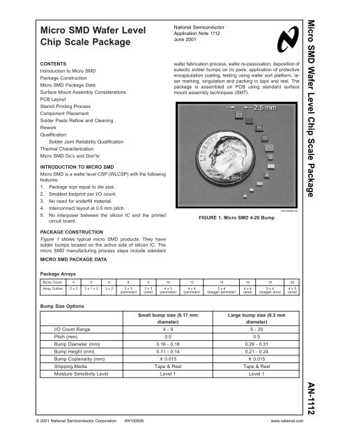
Figure 1 shows typical micro <strong>SMD</strong> products. They have<br />
solder bumps located on the active side of silicon IC. The<br />
micro <strong>SMD</strong> manufacturing process steps include standard<br />
MICRO <strong>SMD</strong> PACKAGE DATA<br />
<strong>Package</strong> Arrays<br />
wafer fabrication process, wafer re-passivation, deposition of<br />
eutectic solder bumps on i/o pads, application of protective<br />
encapsulation coating, testing using wafer sort platform, laser<br />
marking, singulation and packing in tape and reel. The<br />
package is assembled on PCB using standard surface<br />
mount assembly techniques (SMT).<br />
Bump Count 4 5 6 8 9 10 12 14 16 18 20<br />
Array Outline 2 x 2 2x1x2 3x2 3x3<br />
(perimeter)<br />
Bump Size Options<br />
3x3<br />
(area)<br />
4x3<br />
(perimeter)<br />
4x4<br />
(perimeter)<br />
Small bump size (0.17 mm<br />
diameter)<br />
National Semiconductor<br />
<strong>Application</strong> <strong>Note</strong> <strong>1112</strong><br />
June 2001<br />
FIGURE 1. <strong>Micro</strong> <strong>SMD</strong> 4-20 Bump<br />
5x4<br />
(stagger perimeter)<br />
4x4<br />
(area)<br />
5x4<br />
(stagger area)<br />
Large bump size (0.3 mm<br />
diameter)<br />
I/O Count Range 4 - 9 5 - 20<br />
Pitch (mm) 0.5 0.5<br />
Bump Diameter (mm) 0.16 - 0.18 0.29 - 0.31<br />
Bump Height (mm) 0.11 - 0.14 0.21 - 0.24<br />
Bump Coplanarity (mm) ± 0.015 ± 0.015<br />
Shipping Media Tape & Reel Tape & Reel<br />
Moisture Sensitivity <strong>Level</strong> <strong>Level</strong> 1 <strong>Level</strong> 1<br />
AN100926-46<br />
4x5<br />
(area)<br />
<strong>Micro</strong> <strong>SMD</strong> <strong>Wafer</strong> <strong>Level</strong> <strong>Chip</strong> <strong>Scale</strong> <strong>Package</strong> AN-<strong>1112</strong><br />
© 2001 National Semiconductor Corporation AN100926 www.national.com
AN-<strong>1112</strong><br />
SURFACE MOUNT ASSEMBLY CONSIDERATIONS<br />
<strong>Micro</strong> <strong>SMD</strong> surface mount assembly operations include,<br />
• Printing solder paste on PCB.<br />
• Component placement using standard pick and place<br />
equipment.<br />
• Solder reflow and cleaning (depending on flux type).<br />
Advantages of micro <strong>SMD</strong> during SMT assembly include,<br />
• Standard tape and reel shipping media eases handling<br />
issues (per EIA-481-1)<br />
• Uses standard SMT pick and place equipment.<br />
• Standard reflow process.<br />
PCB LAYOUT<br />
Two types of land patterns are used for surface mount<br />
packages,<br />
1. Non-solder mask defined (N<strong>SMD</strong>)<br />
2. Solder mask defined (<strong>SMD</strong>).<br />
FIGURE 2. N<strong>SMD</strong> and <strong>SMD</strong> Pad Definition<br />
AN100926-5<br />
1. N<strong>SMD</strong> configuration is preferred due to its tighter control on copper etch process and a reduction in the stress concentration<br />
points on the PCB side compared to <strong>SMD</strong> configuration.<br />
2. A copper layer thickness of less than 1 oz is recommended to achieve higher stand-off. A 1 oz. (30 micron) or greater copper<br />
thickness results in a lowering of the effective stand-off, which may compromise solder joint reliability.<br />
3. For the N<strong>SMD</strong> pad geometry, the trace width at the connection to the land pad should not exceed 2/3 of the pad diameter.<br />
The recommended pad geometry is shown in Table 1.<br />
TABLE 1. Recommended PCB Pad Geometry<br />
Small Bump Size (0.17 mm Diameter)<br />
Large Bump Size (0.3 mm Diameter)<br />
Pad Definition Copper Pad Solder Mask Opening Copper Pad Solder Mask Opening<br />
N<strong>SMD</strong> 0.175 +0.0/−0.025 mm 0.350 ± 0.025 mm 0.275 +0.0/−0.025 mm 0.375 ± 0.025 mm<br />
<strong>SMD</strong> 0.350 ± 0.025 mm 0.175 ± 0.025 mm 0.375 +0.0/−0.025 mm 0.275 ± 0.025 mm<br />
For PCB layouts employing via-in-pad structures (micro-via),<br />
N<strong>SMD</strong> pad definition should be used, since this ensures<br />
adequate wetting area on the copper pads and hence a<br />
better joint.<br />
Organic solderability preservative coating (OSP) board finish<br />
is used for internal characterization.<br />
Allowable board finishes are Copper-OSP and Nickel-Gold.<br />
• For Ni-Au (electroplated Nickel, immersion Gold) gold<br />
thickness must be less than 0.5 microns to avoid solder<br />
joint embrittlement.<br />
• The fan-out for the traces should be symmetrical across<br />
X and Y directions to avoid part rotation due to surface<br />
tension of solder.<br />
• HASL (Hot Air Solder <strong>Level</strong>ed) board finish is not recommended.<br />
STENCIL PRINTING PROCESS<br />
• Use laser cutting followed by electro-polishing for stencil<br />
fabrication.<br />
• The recommended stencil apertures are shown in Table<br />
2.<br />
• If possible, offset apertures from land pads to maximize<br />
separation and minimize possibility of bridging for micro<br />
<strong>SMD</strong> packages with less than 10 bump counts and using<br />
small bump size. No print offset is required for higher<br />
bump counts and larger bump size.<br />
• Use Type 3 (25 to 45 micron particle size range) or finer<br />
solder paste for printing.<br />
TABLE 2. Recommended Stencil Apertures<br />
Recommended<br />
Stencil<br />
Aperture Size<br />
0.17 mm<br />
Diameter<br />
Solder Bump<br />
0.3 x 0.3 mm<br />
square, 0.125<br />
mm thick<br />
0.3 mm<br />
Diameter<br />
Solder Bump<br />
0.25 x 0.25 mm<br />
square, 0.125<br />
mm thick<br />
www.national.com 2
COMPONENT PLACEMENT<br />
Standard pick-and-place machines can be used for placing<br />
the micro <strong>SMD</strong>. Either of the following methods can be used<br />
for recognition and positioning.<br />
1. Vision system to locate package silhouette.<br />
2. Vision system to locate individual bumps (slower and<br />
more expensive).<br />
Other features of micro <strong>SMD</strong> placement are,<br />
1. It is preferable to use IC placement/fine pitch placement<br />
machines over chip-shooters for better accuracy.<br />
2. <strong>Micro</strong> <strong>SMD</strong> solder bumps self-align when placed at an<br />
offset due to selfcentering nature of solder bumps.<br />
3. Though micro <strong>SMD</strong> can withstand a placement force of<br />
up to 1 kg for 0.5 seconds, little or no force needs to be<br />
exerted during placement. It is recommended that<br />
bumps be dipped into solder paste on PCB to greater<br />
than 20% of paste block height.<br />
SOLDER PASTE REFLOW AND CLEANING<br />
• <strong>Micro</strong> <strong>SMD</strong> is compatible with industry standard reflow<br />
process.<br />
• It is recommended to use Nitrogen purge during reflow.<br />
• <strong>Micro</strong> <strong>SMD</strong> is qualified for up to three reflow operations<br />
(235˚ C peak) per J-STD-020.<br />
• <strong>Micro</strong> <strong>SMD</strong> can withstand peak reflow temperatures of<br />
260˚ C for up to 30 seconds.<br />
REWORK<br />
The key features for the micro <strong>SMD</strong> rework are listed below.<br />
1. Rework procedure used is identical to the one used for<br />
most BGA and CSP packages.<br />
2. Rework reflow process should duplicate original reflow<br />
profile used for assembly.<br />
3. Rework system should include localized convection<br />
heating element with profiling capability, a bottom side<br />
pre-heater and a part pick and placer with image overlay.<br />
4. A rework demo video is available from National Semiconductor<br />
at http://www.national.com/appinfo/microsmd.<br />
QUALIFICATION<br />
The following sections describe solder joint reliability qualification<br />
and mechanical testing results for micro <strong>SMD</strong> when<br />
mounted on FR-4 PCB. Testing included use of daisy chain<br />
components. Product reliability data is included in respective<br />
product qualification reports.<br />
Solder Joint Reliability Qualification<br />
1. TEMPERATURE CYCLING: Testing performed per<br />
IPC-SM-785 Guidelines for Accelerated Reliability Testing of<br />
Surface Mount Solder Attachments. The results of this testing<br />
after following the above mentioned assembly conditions<br />
described here are shown in Figure 3, Figure 4 and Table 3.<br />
AN-<strong>1112</strong><br />
AN100926-13<br />
FIGURE 3. −40˚C to 125˚C, 1 cycle/hr Temperature Cycling Profile per IPC-SM-785<br />
3<br />
www.national.com
AN-<strong>1112</strong><br />
FIGURE 4. Impact of PCB Pad Size on Reliability for 0.17 mm Bump <strong>Package</strong><br />
AN100926-45<br />
TABLE 3. Temperature Cycling of <strong>Micro</strong> <strong>SMD</strong> Devices<br />
<strong>Micro</strong> <strong>SMD</strong> Assembly Stencil Type Test Condition 0 cycles 284 cycles 764 cycles 1056 cycles 1152 cycles<br />
8 bump<br />
0.17 mm bump diameter<br />
8 bump<br />
0.17 mm bump diameter<br />
0.100 mm thick<br />
0.250 x 0.300 mm<br />
Oval aperture<br />
0.125 mm thick<br />
0.300 x 0.300 mm<br />
Square aperture<br />
−40 to 125˚ C, 1 cycle/hr, 25 min dwell, 5<br />
min transfer<br />
0/32 0/32 0/32 4/32 5/32<br />
0/32 0/32 0/32 0/32 0/32<br />
<strong>Micro</strong> <strong>SMD</strong> Assembly Stencil Type Test Condition 0 cycles 300 cycles 600 cycles 624 cycles 924 cycles 1224 cycles<br />
18 Bump<br />
0.3 mm bump diameter<br />
0.125 mm thick<br />
0.300 x 0.300 mm<br />
Square aperture<br />
−40 to 125˚ C, 1 cycle/hr, 15 min dwell, 15<br />
min ramp<br />
0/102 0/102 0/102 0/102 0/102 0/102<br />
2. PACKAGE SHEAR: As part of the manufacturing process,<br />
bump shear data is collected at package level to ensure<br />
attachment of solder ball to the package. The average package<br />
shear strength recorded was approximately 100 gm per<br />
solder joint for 0.17 mm diameter solder bump. For the 0.3<br />
mm diameter solder bump, the package shear was greater<br />
than 200 gm per solder joint. Measured value of package<br />
shear may vary depending on materials and methods used<br />
in surface mount assembly.<br />
3. PULL TEST: Assembled micro <strong>SMD</strong> 8 bump units were<br />
pulled vertically upward with a stud machined into the back<br />
of the component. Component was pulled till it was removed<br />
off the board. Average stud pull strength was recorded as 80<br />
gm per solder joint for 0.17 mm diameter solder bump.<br />
www.national.com 4
AN-<strong>1112</strong><br />
AN100926-38<br />
FIGURE 5. Pull Test Carried Out on the <strong>SMD</strong> 8 Bump (0.17 mm Diameter Bump)<br />
4. DROP TEST: Drop test results are shown in Table 4. The<br />
tests were carried out on micro <strong>SMD</strong> 8 bump packages (0.17<br />
mm diameter bump) mounted on 1.5 mm thick PCB. It<br />
included 7 drops on first edge, 7 on second edge, 8 drops on<br />
the corner and 8 drops on flat face, a total of 30 drops. An<br />
increase of 10% or more in daisy chain loop resistance was<br />
considered as a failure.<br />
TABLE 4. <strong>Micro</strong> <strong>SMD</strong> Drop Test Results (0.17 mm Diameter Bump <strong>Package</strong>)<br />
Weight<br />
Test Results (Failures after 30 drops)<br />
Length 1m 1.5m 2m<br />
75 gm 0/8 0/8 0/8<br />
150 gm 0/8 0/8 0/8<br />
5. THREE-POINT BEND TEST: The three-point bend test<br />
used a test board with a 100 mm span. Deflection was<br />
applied at the center at 9.45 mm/min. No solder joint failure<br />
was observed even with deflections as high as 25 mm.<br />
AN100926-17<br />
FIGURE 6. Board Deflection and Net Resistance (0.17 mm Diameter Bump <strong>Package</strong>)<br />
THERMAL CHARACTERIZATION<br />
Thermal performance of micro <strong>SMD</strong> packages was assessed<br />
using low effective thermal conductivity test boards<br />
per EIA/JESD51-3. The performance of the <strong>SMD</strong> product<br />
depends on product die size and application (PCB layout<br />
and design), and the details of Theta JA values are available<br />
in product data sheets at http://www.national.com .<br />
5<br />
www.national.com
AN-<strong>1112</strong><br />
MICRO <strong>SMD</strong> DO’S and DONT’S<br />
SMALL BUMP<br />
DO’s<br />
DONT’s<br />
PCB 150 µm < Pad Dia < 200 µm Pad Dia < 150 µm or Pad Dia<br />
> 200 µm<br />
Stencil<br />
Solder Paste<br />
Prefer non-solder mask<br />
defined (N<strong>SMD</strong>) over solder<br />
mask defined (<strong>SMD</strong>). Solder<br />
mask opening ≤ 350 µm<br />
round.<br />
Organic Solderability<br />
Preservative (OSP) or Ni-Au<br />
surface finish (Less than 0.5<br />
µm Au thickness).<br />
300 µm x 300 µm square<br />
aperture<br />
Laser cut + electro-polished or<br />
Additive build-up<br />
100 µm < Thickness < 125<br />
µm<br />
Type 3 (25 to 45 µm particle<br />
size range) or finer<br />
Solder mask opening > 375<br />
µm round.<br />
Greater than 0.5 µm Au<br />
thickness for Ni-Au surface<br />
finish.<br />
HASL (Hot Air Solder<br />
<strong>Level</strong>ed) board finish.<br />
Less than 275 x 275 µm<br />
square aperture<br />
Greater than 300 µm x 300<br />
µm square aperture<br />
Chemical etch<br />
Thickness > 125 µm or < 100<br />
µm<br />
Type 2 or Type 1<br />
LARGE BUMP<br />
DO’s<br />
DONT’s<br />
PCB 250 µm < Pad Dia < 275 µm Pad Dia < 250 µm or Pad Dia<br />
> 275 µm<br />
Stencil<br />
Solder Paste<br />
Prefer non-solder mask<br />
defined (N<strong>SMD</strong>) over solder<br />
mask defined (<strong>SMD</strong>). Solder<br />
mask opening ≤ 375 µm<br />
round.<br />
Organic Solderability<br />
Preservative (OSP) or Ni-Au<br />
surface finish (Less than 0.5<br />
µm Au thickness).<br />
250 µm x 250 µm square<br />
aperture<br />
Laser cut + electro-polished or<br />
Additive build-up<br />
100 µm < Thickness < 125<br />
µm<br />
Type 3 (25 to 45 µm particle<br />
size range) or finer<br />
Solder mask opening > 375<br />
µm round.<br />
Greater than 0.5 µm Au<br />
thickness for Ni-Au surface<br />
finish.<br />
HASL (Hot Air Solder<br />
<strong>Level</strong>ed) board finish.<br />
Less than 200 x 200 µm<br />
square aperture<br />
Greater than 275 µm x 275<br />
µm square aperture<br />
Chemical etch<br />
Thickness > 125 µm or<br />
Thickness < 100 µm<br />
Type 2 or Type 1<br />
www.national.com 6
LIFE SUPPORT POLICY<br />
<strong>Note</strong>s<br />
NATIONAL’S PRODUCTS ARE NOT AUTHORIZED FOR USE AS CRITICAL COMPONENTS IN LIFE SUPPORT<br />
DEVICES OR SYSTEMS WITHOUT THE EXPRESS WRITTEN APPROVAL OF THE PRESIDENT AND GENERAL<br />
COUNSEL OF NATIONAL SEMICONDUCTOR CORPORATION. As used herein:<br />
1. Life support devices or systems are devices or<br />
systems which, (a) are intended for surgical implant<br />
into the body, or (b) support or sustain life, and<br />
whose failure to perform when properly used in<br />
accordance with instructions for use provided in the<br />
labeling, can be reasonably expected to result in a<br />
significant injury to the user.<br />
National Semiconductor<br />
Corporation<br />
Americas<br />
Email: support@nsc.com<br />
www.national.com<br />
National Semiconductor<br />
Europe<br />
Fax: +49 (0) 180-530 85 86<br />
Email: europe.support@nsc.com<br />
Deutsch Tel: +49 (0) 69 9508 6208<br />
English Tel: +44 (0) 870 24 0 2171<br />
Français Tel: +33 (0) 1 41 91 8790<br />
2. A critical component is any component of a life<br />
support device or system whose failure to perform<br />
can be reasonably expected to cause the failure of<br />
the life support device or system, or to affect its<br />
safety or effectiveness.<br />
National Semiconductor<br />
Asia Pacific Customer<br />
Response Group<br />
Tel: 65-2544466<br />
Fax: 65-2504466<br />
Email: ap.support@nsc.com<br />
National Semiconductor<br />
Japan Ltd.<br />
Tel: 81-3-5639-7560<br />
Fax: 81-3-5639-7507<br />
<strong>Micro</strong> <strong>SMD</strong> <strong>Wafer</strong> <strong>Level</strong> <strong>Chip</strong> <strong>Scale</strong> <strong>Package</strong> AN-<strong>1112</strong><br />
National does not assume any responsibility for use of any circuitry described, no circuit patent licenses are implied and National reserves the right at any time without notice to change said circuitry and specifications.