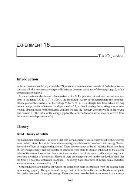
EXPERIMENT 16 The PN junction Introduction Theory
EXPERIMENT 16 The PN junction Introduction Theory
EXPERIMENT 16 The PN junction Introduction Theory

You also want an ePaper? Increase the reach of your titles
YUMPU automatically turns print PDFs into web optimized ePapers that Google loves.
<strong>EXPERIMENT</strong> <strong>16</strong><br />
<strong>The</strong> <strong>PN</strong> <strong>junction</strong><br />
<strong>Introduction</strong><br />
In this experiment on the physics of the <strong>PN</strong> <strong>junction</strong>, a determination is made of both the universal<br />
constant e/k (i.e. elementary charge to Boltzmann constant ratio) and of the energy gap E g of the<br />
semiconductor material.<br />
In the experiment the forward characteristics of a Si <strong>PN</strong> <strong>junction</strong>, at various constant temperatures<br />
in the range 150 K < T < 300 K, are measured. At any given temperature the semilogarithmic<br />
plot of the current I, vs the voltage V, for V ≫ kT , is a straight line from which we may<br />
extract two quantities of interest: its slope equals e/kT, so that, knowing the working temperature,<br />
we may obtain a value for the universal constant e/k, and the intercept gives the value of the reverse<br />
bias current I 0 . <strong>The</strong> value of the energy gap for the semiconductor material may be derived from<br />
the temperature dependence of I 0 .<br />
<strong>The</strong>ory<br />
Band <strong>The</strong>ory of Solids<br />
From quantum mechanics it is known that only certain energy states are permitted to the electrons<br />
in an isolated atom. In a solid, these discrete energy levels become broadened into energy ‘bands’<br />
due to the effects of neighbouring atoms. <strong>The</strong>re are two types of band. Valence bands are those<br />
of low enough energy that the transfer of electrons from atom to atom is inhibited by the electric<br />
fields of the atoms. Conduction bands are those in which the electrons are sufficiently energetic to<br />
overcome the fields of the atoms. Hence, if there are charge carriers in the conduction band they<br />
can flow if a potential difference is applied. <strong>The</strong> energy band structures of metals, semiconductors<br />
and insulators are shown in Fig. <strong>16</strong>.1.<br />
Semiconductors are materials in which the conduction band is separated from the valence band<br />
by an energy gap E g . This gap is small enough that electrons from the valence band can jump into<br />
the conduction band if they gain energy. <strong>The</strong>se electrons leave behind vacant states in the valence<br />
<strong>16</strong>-1
Experiment<strong>16</strong>. <strong>The</strong> <strong>PN</strong> <strong>junction</strong><br />
Conduction band<br />
Empty states<br />
Energy gap<br />
Valence band<br />
Occupied states<br />
Insulator<br />
Semiconductor<br />
Figure <strong>16</strong>.1: Schematic diagram of the energy band structures in metals, semiconductors and<br />
insulators.<br />
Metal<br />
band. Once carriers are in the conduction band they can participate in conduction. In insulators,<br />
the gap is too large to be bridged under normal circumstances and hence conductivity is poor.<br />
Doping of semiconductors<br />
<strong>The</strong> electrical conductivity of a semiconductor such as germanium or silicon depends on the concentration<br />
of charge carriers in the conduction band. <strong>The</strong>se may be produced by thermal excitation<br />
of bound valence electrons into the conduction band or by the deliberate addition of impurities into<br />
the semiconductor, in a process known as ‘doping’.<br />
Si<br />
Si<br />
Si<br />
Si<br />
e<br />
P<br />
Si<br />
Si<br />
Si<br />
Figure <strong>16</strong>.2: Schematic diagram of doping.<br />
Fig. <strong>16</strong>.2 illustrates the doping of Group IV Si, which has four valence electrons, by Group V<br />
phosphorous, with five valence electrons. Four of the P valence electrons form covalent bands<br />
with electrons from neighbouring Si atoms. <strong>The</strong> remaining P electron is then loosely bound and<br />
easily energised into the conduction band. <strong>The</strong> Si is now an ‘n-type’ material i.e. it now has<br />
excess negative carriers. Alternatively the Si could be doped with a Group III element such as<br />
boron. <strong>The</strong> 3 valence electrons of boron atoms bond with electrons from neighbouring Si atoms<br />
as before, except this time there is 1 electron short. <strong>The</strong> boron atom therefore acts like a ‘hole’<br />
in that electrons from neighbouring Si atoms may jump into the vacancy in the B atom and it will<br />
appear as if a positive charge is moving through the material. Such a semiconductor is referred to<br />
as a ‘p-type’ material.<br />
<strong>16</strong>-2
Experiment<strong>16</strong>. <strong>The</strong> <strong>PN</strong> <strong>junction</strong><br />
P N P N<br />
Forward bias<br />
Figure <strong>16</strong>.3: Biasing the <strong>PN</strong> <strong>junction</strong>.<br />
Reverse bias<br />
In an n-type semiconductor, the majority carriers are electrons, with a small fraction of the<br />
conductivity due to thermally generated holes (minority carriers). In a p-type material the majority<br />
carriers are holes, with a small fraction of the conductivity due to thermally generated electrons<br />
(minority carriers).<br />
<strong>The</strong> conductivity of Si is increased by a factor 10 3 at room temperature by the addition of 1 B<br />
atom per 10 5 Si atoms.<br />
<strong>The</strong> <strong>PN</strong> <strong>junction</strong><br />
A <strong>PN</strong> <strong>junction</strong> is simply a piece of semiconductor which is doped n-type on one side and p-type<br />
on the other.<br />
In a <strong>PN</strong> <strong>junction</strong> which is forward biased (Fig. <strong>16</strong>.3) the current which flows is almost entirely<br />
due to majority carriers. Under reverse bias however, the current, which is very much smaller than<br />
that which flows under forward bias, is due to thermally generated minority carriers and is strongly<br />
temperature dependent, according to the equation:<br />
I 0 = A exp<br />
( ) −Eg<br />
kT<br />
(<strong>16</strong>.1)<br />
where I 0 is known as the ‘reverse bias saturation current’ and is the maximum minority carrier<br />
current which flows in the reverse biased <strong>PN</strong> <strong>junction</strong>; A is (an almost temperature independent)<br />
constant; E g is the semiconductor bandgap; k is Boltzmann’s constant and T is the temperature<br />
in 0 K. <strong>The</strong> current flow through the <strong>PN</strong> <strong>junction</strong> used in this experiment is well described by the<br />
Shockley equation:<br />
( ) ] eV<br />
I = I 0<br />
[exp − 1<br />
(<strong>16</strong>.2)<br />
kT<br />
where I is the current; V is the voltage applied to the <strong>junction</strong>; e is the electronic charge; I 0 , k and<br />
T are as above.<br />
In order to determine E g from Eq. <strong>16</strong>.1, I 0 as a function of temperature must be measured. To<br />
achieve this the current-voltage characteristic of the <strong>junction</strong> is determined at a number of fixed<br />
temperatures. Taking the natural log of Eq. <strong>16</strong>.2 we get:<br />
ln I = ln I 0 + eV<br />
kT<br />
(<strong>16</strong>.3)<br />
<strong>16</strong>-3
Experiment<strong>16</strong>. <strong>The</strong> <strong>PN</strong> <strong>junction</strong><br />
Figure <strong>16</strong>.4: <strong>The</strong> forward bias characteristics of the Si transdiode at four different temperatures.<br />
By plotting ln I vs V (see Fig. <strong>16</strong>.4) and determining the best fit slope (and error on the slope)<br />
for each value of T , a number of estimates of e/k can be made. <strong>The</strong> mean value and the error<br />
on this mean should also be calculated. For each characteristic curve the intercept of the best fit<br />
straight line should also be determined. This corresponds to ln(I 0 ). From Eq. <strong>16</strong>.1 we know that<br />
lnI 0 = ln(A) − E g<br />
kT<br />
(<strong>16</strong>.4)<br />
<strong>The</strong>refore plotting ln(I 0 ) vs 1 −Eg<br />
should yield a straight line with slope (Fig. <strong>16</strong>.5). Hence the<br />
T k<br />
bandgap energy E g can be determined. Determine the best fit slope and error and hence calculate<br />
E g and the error on E g . You should quote your result in eV .<br />
Experimental Apparatus<br />
<strong>The</strong> Si used in this experiment is in the form of an npn transistor wired in such a way that its<br />
behaviour accurately follows the Shockley equation (Eq. <strong>16</strong>.2). This yields more accurate results<br />
than using a pn <strong>junction</strong> which only approximately follows the Shockley equation. <strong>The</strong> physics of<br />
the experiment is not changed as a result of using this so-called ‘transiode’ configuration.<br />
<strong>The</strong> sample is mounted in a small copper cell obtained from a thick walled tube, 2 cm in diameter<br />
and 5 cm long. <strong>The</strong> copper cell bottom is soft soldered to a brass rod which acts as a cold finger,<br />
when its low end is dipped into a liquid nitrogen bath. A 30 Ω constantan wire heater is wound<br />
around the upper end of the brass rod. An integrated circuit temperature transducer (AD590) is<br />
glued onto the cell bottom, to be used as a sensor for the thermoregulator that drives the heater.<br />
<strong>The</strong> temperature is measured by type K thermocouple whose signal is read on a digital multimeter.<br />
<strong>The</strong> thermocouple <strong>junction</strong> is thermally anchored to the sample by means of few turns of PTFE<br />
tape wrapped around the transistor case. All the electrical connections are made by thin wires<br />
<strong>16</strong>-4
Experiment<strong>16</strong>. <strong>The</strong> <strong>PN</strong> <strong>junction</strong><br />
Figure <strong>16</strong>.5: <strong>The</strong> values of the inverse current I 0 , extrapolated from the forward characteristics<br />
measured at various temperatures, plotted vs 1/T . <strong>The</strong> line represents the linear best fit.<br />
fed into the cell through a thin walled stainless steel tube soldered to the copper cell. <strong>The</strong> cell is<br />
suspended by the steel tube inside a dewar vessel (see Fig. <strong>16</strong>.6).<br />
To measure the forward characteristics of the transdiode a current-voltage converter with a fieldeffect<br />
transistor input op-amp is used which can reliably measure currents as small as 10 −11 A.<br />
<strong>The</strong> sample is thermoregulated by means of a simple circuit. <strong>The</strong> temperature sensor AD590<br />
produces an output current of 1 µA/K, that is converted into a signal voltage V T (10 mV/K) by a<br />
current to voltage converter.<br />
Experimental Procedure<br />
Note:<br />
Please be careful when handling liquid nitrogen and<br />
follow the safety instructions at all times.<br />
<strong>The</strong> main experimental task is to determine the I −V characteristics of the Si sample over a range<br />
of preset temperatures. At the beginning of the laboratory session, carefully lower the measuring<br />
cell into the liquid N 2 dewar, until 3/4 of the brass rod is immersed in liquid N 2 . Set the preset<br />
temperature value to 150 K. <strong>The</strong> cell will take approximately 20 minutes to cool down to this<br />
temperature and the thermoregulator in the cell will ensure it remains at the preset value. Once<br />
the temperature has stabilised you should increase the bias voltage and record both your voltage<br />
and current readings. Change the current scale as necessary, remembering to record the scale<br />
factor. <strong>The</strong> temperature value on the front panel should not be used as a measure of the sample<br />
temperature. Instead the sample temperature should be measured from the thermocouple, which is<br />
directly attached to the sample, using the digital voltmeter. You should use the conversion chart<br />
provided to convert from thermocouple voltage to sample temperature. This is the temperature<br />
<strong>16</strong>-5
Experiment<strong>16</strong>. <strong>The</strong> <strong>PN</strong> <strong>junction</strong><br />
To measurement<br />
box<br />
To temperature<br />
control box<br />
To multimeter<br />
Copper cell<br />
Transdiode<br />
<strong>The</strong>rmocouple<br />
AD590<br />
<strong>The</strong>rmos<br />
flask<br />
Heater<br />
Liquid N2<br />
Figure <strong>16</strong>.6: <strong>The</strong> measuring cell.<br />
value to be used in your analysis. It is a more accurate estimate of the sample temperature than<br />
the preset cell temperature, which is measuring the temperature in the cell, rather than the sample<br />
temperature.<br />
You should take data for at least 4 characteristic curves over a range of temperatures from<br />
150 K to 350 K.<br />
Experimental Results and Data Analysis<br />
<strong>The</strong> forward characteristics, measured at several temperatures with the Si transdiode, is shown in<br />
semilogarithmic plot of Fig. <strong>16</strong>.4, proving that the linear behavior predicted by Eq. <strong>16</strong>.2 is obeyed,<br />
without appreciable deviation, in a very wide current range (i.e. from I=10 −11 A up to 10 −3 A).<br />
Plot your data as shown in Fig. <strong>16</strong>.4 and verify the validity of Eq. <strong>16</strong>.2.<br />
From the values of the slope S of the forward characteristics in Fig. <strong>16</strong>.4, obtained by a straight<br />
line least squares fit, and the measured temperature T , we get the values for the ratio e/k = ST .<br />
Estimate the mean (and error) on your measurement of e/k.<br />
How does your value compare with the accepted value for e/k of 1<strong>16</strong>04 ± 0.6 CK J −1 ?<br />
<strong>The</strong> intercept with the V = 0 axis of the logarithmic characteristic gives the value of I 0 at the<br />
working temperature: therefore from several runs performed at various constant temperatures we<br />
may get a measurement of the temperature dependence of I 0 (T ), to be compared with the one<br />
predicted by Eq. <strong>16</strong>.1.<br />
<strong>The</strong> result of this procedure is shown in Fig. <strong>16</strong>.5, where each point represents the I 0 value<br />
extrapolated from an isothermal run like those reported in Fig. <strong>16</strong>.4.<br />
Fig. <strong>16</strong>.5 shows that the plot of ln I 0 vs 1/T is essentially a straight line: this is the behavior<br />
predicted by Eq. <strong>16</strong>.4 from which we expect a slope −E g /k.<br />
By fitting the experimental points simply with a straight line you should determine a value for<br />
E g . <strong>The</strong> error can be evaluated assuming ∆T =1 K and ∆ln(I 0 )=0.1. How does your value compare<br />
<strong>16</strong>-6
Experiment<strong>16</strong>. <strong>The</strong> <strong>PN</strong> <strong>junction</strong><br />
with the accepted value for the bandgap of Si which is 1.217 ± 0.018 eV?<br />
References<br />
1. ‘<strong>Introduction</strong> to the Physics of Electrons in Solids’, Brian K. Tanner<br />
2. ‘Physics for Computer Science Students’, N. Garcia and A.C. Damask<br />
3. EP 2.4<br />
4. ‘Experiment on the physics of the <strong>PN</strong> <strong>junction</strong>’, Sconza, Torzo, Viola, American Journal of<br />
Physics, Vol. 62, pp.66, 1994<br />
WWW :<br />
• Britney Spears’ guide to semiconductor physics - http://britneyspears.ac/lasers.htm<br />
• <strong>The</strong> semiconductor applet service - http://jas2.eng.buffalo.edu/applets/index.html<br />
<strong>16</strong>-7