E2V CCD47-10
E2V CCD47-10
E2V CCD47-10

You also want an ePaper? Increase the reach of your titles
YUMPU automatically turns print PDFs into web optimized ePapers that Google loves.
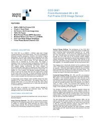
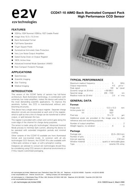
<strong>CCD47</strong>-<strong>10</strong> AIMO Back Illuminated Compact Pack<br />
High Performance CCD Sensor<br />
FEATURES<br />
* <strong>10</strong>24 by <strong>10</strong>24 Nominal (<strong>10</strong>56 by <strong>10</strong>27 Usable Pixels)<br />
* Image Area 13.3 x 13.3 mm<br />
* Back Illuminated Format<br />
* Full-Frame Operation<br />
* 13 mm Square Pixels<br />
* Symmetrical Anti-static Gate Protection<br />
* Very Low Noise Output Amplifiers<br />
* Gated Dump Drain on Output Register<br />
* <strong>10</strong>0% Active Area<br />
* Advanced Inverted Mode Operation (AIMO)<br />
* New Compact Footprint Package<br />
APPLICATIONS<br />
* Spectroscopy<br />
* Scientific Imaging<br />
* Star Tracking<br />
* Medical Imaging<br />
INTRODUCTION<br />
This version of the <strong>CCD47</strong> family of sensors has full-frame<br />
architecture. Back illumination technology, in combination with<br />
extremely low noise amplifiers, makes the device well suited to<br />
the most demanding scientific applications. To improve the<br />
sensitivity further, the CCD is manufactured without antiblooming<br />
structures.<br />
This device has a single serial output register. Separate charge<br />
detection circuits are incorporated at each end of the register,<br />
which is split so that a line of charge can be transferred to either<br />
output, or split between the two.<br />
The register is provided with a drain and control gate along the<br />
outer edge of the channel for charge dump purposes.<br />
The sensor is made using e2v technologies’ Advanced Inverted<br />
Mode process to minimise dark current, allowing the device to<br />
be operated with extended integration periods and minimal<br />
cooling.<br />
Other variants of the <strong>CCD47</strong>-<strong>10</strong> available are front illuminated<br />
format and non-inverted mode. In common with all e2v<br />
technologies CCD Sensors, the <strong>CCD47</strong>-<strong>10</strong> is also available with<br />
a fibre-optic window or taper, or with a phosphor coating.<br />
Designers are advised to consult e2v technologies should they<br />
be considering using CCD sensors in abnormal environments or<br />
if they require customised packaging.<br />
TYPICAL PERFORMANCE<br />
Maximum readout frequency . . . . . 5 MHz<br />
Output responsivity . . . . . . . . 4.5 mV/e 7<br />
Peak signal . . . . . . . . . . . <strong>10</strong>0 ke 7 /pixel<br />
Dynamic range (at 20 kHz) . . . *50 000:1<br />
Spectral range . . . . . . . 200 – 1<strong>10</strong>0 nm<br />
Readout noise (at 20 kHz) . . . . . . 2.0 e 7 rms<br />
GENERAL DATA<br />
Format<br />
Image area . . . . . . . . . 13.3 x 13.3 mm<br />
Active pixels (H) . . . . . . . . <strong>10</strong>56<br />
(V) . . . . . . . . <strong>10</strong>27<br />
Pixel size . . . . . . . . . . 13 x 13 mm<br />
Additional pixels are provided in the image area for dark<br />
reference and over-scanning purposes.<br />
Number of output amplifiers . . . . . . . . . . 2<br />
Weight (approx, no window) . . . . . 6 g<br />
Package<br />
Package size . . . . . . . . . . . 22.6 x 29.9 mm<br />
Number of pins . . . . . . . . . . . . . . 24<br />
Inter-pin spacing . . . . . . . . . . . 2.54 mm<br />
Window material . . . . . . quartz or removable glass<br />
Type . . . . . . . . . . . . ceramic DIL array<br />
e2v technologies (uk) limited, Waterhouse Lane, Chelmsford, Essex CM1 2QU, UK Telephone: +44 (0)1245 493493 Facsimile: +44 (0)1245 492492<br />
e-mail: enquiries@e2v.com Internet: www.e2v.com Holding Company: e2v technologies plc<br />
e2v technologies inc. 4 Westchester Plaza, PO Box 1482, Elmsford, NY<strong>10</strong>523-1482 USA Telephone: (914) 592-6050 Facsimile: (914) 592-5148<br />
e-mail: enquiries@e2vtechnologies-na.com<br />
# e2v technologies (uk) limited 2006 A1A-<strong>10</strong>0029 Issue 5, March 2006<br />
411/9572
PERFORMANCE<br />
Min Typical Max<br />
Peak charge storage (see note 1) 60k <strong>10</strong>0k – e 7 /pixel<br />
Peak output voltage (no binning) – 450 – mV<br />
Dark signal at 293 K (see notes 2 and 3) – 250 500 e 7 /pixel/s<br />
Dynamic range (see note 4) – 50 000 –<br />
Charge transfer efficiency (see note 5):<br />
parallel<br />
serial<br />
–<br />
–<br />
99.9999<br />
99.9993<br />
Output amplifier responsivity (see note 3) 3.0 4.5 6.0 mV/e 7<br />
Readout noise at 253 K (see notes 3 and 6) – 2.0 4.0 rms e 7 /pixel<br />
Maximum readout frequency (see note 7) – 5.0 – MHz<br />
Dark signal non-uniformity at 293 K<br />
(std. deviation) (see notes 3 and 8) – 60 125 e 7 /pixel/s<br />
–<br />
–<br />
%<br />
%<br />
Spectral Response (at 253 K)<br />
Wavelength<br />
(nm)<br />
Minimum Response (QE)<br />
UV Coated Midband Coated Broadband Coated Uncoated<br />
Maximum Response<br />
Non-uniformity (1s)<br />
300 45 not specified not specified not specified – %<br />
350 45 15 25 <strong>10</strong> 5 %<br />
400 55 40 55 25 3 %<br />
500 60 85 75 55 3 %<br />
650 60 85 75 50 3 %<br />
900 30 30 30 30 5 %<br />
ELECTRICAL INTERFACE CHARACTERISTICS<br />
Electrode capacitances (measured at mid-clock level)<br />
Min Typical Max<br />
I1/I1 interphase – 3.5 – nF<br />
I1/SS – 4.5 – nF<br />
R1/R1 interphase – 40 – pF<br />
R1/(SS+DG+OD) – 60 – pF<br />
1R/SS – <strong>10</strong> – pF<br />
Output impedance (at typ. operating condition) – 300 – O<br />
NOTES<br />
1. Signal level at which resolution begins to degrade.<br />
2. Measured between 253 and 293 K and V SS +9.5 V. Dark<br />
signal at any temperature T (kelvin) may be estimated from:<br />
Q d /Q d0 = 1.14 x <strong>10</strong> 6 T 3 e 79080/T<br />
where Q d0 is the dark signal at T = 293 K (20 8C).<br />
3. Test carried out at e2v technologies on all sensors.<br />
4. Dynamic range is the ratio of full-well capacity to readout<br />
noise measured at 253 K and 20 kHz readout speed.<br />
5. CCD characterisation measurements made using charge<br />
generated by X-ray photons of known energy.<br />
6. Measured using a dual-slope integrator technique (i.e.<br />
correlated double sampling) with a 20 ms integration period.<br />
7. Readout at speeds in excess of 5 MHz into a 15 pF load can<br />
be achieved but performance to the parameters given<br />
cannot be guaranteed.<br />
8. Measured between 253 and 293 K, excluding white defects.<br />
<strong>10</strong>0029, page 2 # e2v technologies
BLEMISH SPECIFICATION<br />
Traps<br />
Pixels where charge is temporarily held.<br />
Traps are counted if they have a capacity<br />
greater than 200 e 7 at 253 K.<br />
Slipped columns Are counted if they have an amplitude<br />
greater than 200 e 7 .<br />
Black spots Are counted when they have a signal level<br />
of less than 80% of the local mean at a<br />
signal level of approximately half full-well.<br />
White spots Are counted when they have a generation<br />
rate 125 times the specified maximum dark<br />
signal generation rate (measured between<br />
253 and 293 K). The typical temperature<br />
dependence of white spot defects is different<br />
from that of the average dark signal<br />
and is given by:<br />
Q d /Q d0 = 122T 3 e 76400/T<br />
White column<br />
Black column<br />
A column which contains at least 21 white<br />
defects.<br />
A column which contains at least 21 black<br />
defects.<br />
GRADE 0 1 2<br />
Column defects:<br />
black or slipped 0 2 6<br />
white 0 0 2<br />
Black spots 50 <strong>10</strong>0 200<br />
Traps 4200 e 7 2 5 12<br />
White spots 50 80 <strong>10</strong>0<br />
Grade 5 Devices which are fully functioning, with<br />
image quality below that of grade 2, and<br />
which may not meet all other performance<br />
parameters.<br />
Note The effect of temperature on defects is that traps will be<br />
observed less at higher temperatures but more may appear<br />
below 253 K. The amplitude of white spots and columns will<br />
decrease rapidly with temperature.<br />
TYPICAL OUTPUT CIRCUIT NOISE<br />
(Measured using clamp and sample)<br />
V SS = 9.5 V V RD =17V V OD =29V<br />
7<br />
7508<br />
6<br />
NOISE EQUIVALENT SIGNAL (e 7 rms)<br />
5<br />
4<br />
3<br />
2<br />
1<br />
0<br />
<strong>10</strong>k 50k <strong>10</strong>0k 500k 1M<br />
FREQUENCY (Hz)<br />
# e2v technologies <strong>10</strong>0029, page 3
TYPICAL SPECTRAL RESPONSE (At 720 8C, no window)<br />
<strong>10</strong>0<br />
7834<br />
90<br />
80<br />
BROADBAND COATED<br />
MIDBAND COATED<br />
70<br />
UV COATED<br />
60<br />
UNCOATED<br />
50<br />
40<br />
30<br />
QUANTUM EFFICIENCY (%)<br />
20<br />
<strong>10</strong><br />
0<br />
200 300 400 500 600 700 800 900 <strong>10</strong>00 1<strong>10</strong>0<br />
WAVELENGTH (nm)<br />
TYPICAL VARIATION OF DARK SIGNAL WITH SUBSTRATE VOLTAGE<br />
<strong>10</strong> 6<br />
<strong>10</strong> 5<br />
7835<br />
DARK SIGNAL AT 293 K (e 7 /pixel/s)<br />
<strong>10</strong> 4<br />
<strong>10</strong> 3<br />
TYPICAL RANGE<br />
<strong>10</strong> 2<br />
<strong>10</strong> 0 1 2 3 4 5 6 7 8 9 <strong>10</strong> 11 12<br />
SUBSTRATE VOLTAGE V SS (V)<br />
<strong>10</strong>0029, page 4 # e2v technologies
TYPICAL VARIATION OF DARK SIGNAL WITH TEMPERATURE (V SS = +9.5 V)<br />
<strong>10</strong> 4<br />
7329A<br />
<strong>10</strong> 3<br />
<strong>10</strong> 2<br />
<strong>10</strong><br />
DARK SIGNAL (e 7 /pixel/s)<br />
<strong>10</strong> 71<br />
<strong>10</strong> 72 1<br />
740 720 0 20 40<br />
PACKAGE TEMPERATURE (8C)<br />
DEVICE SCHEMATIC<br />
7889<br />
ABD<br />
1<br />
24<br />
ABG<br />
I13<br />
2<br />
23<br />
I13<br />
I12<br />
3<br />
22<br />
I12<br />
I11<br />
4<br />
21<br />
I11<br />
OG<br />
5<br />
6<br />
IMAGE SECTION<br />
<strong>10</strong>56 x <strong>10</strong>27 ACTIVE PIXELS<br />
13 x 13 mm<br />
20<br />
19<br />
DG<br />
SS<br />
7<br />
18<br />
SS<br />
1R<br />
8<br />
8 8<br />
17<br />
R13<br />
R12L<br />
R11L<br />
OD<br />
9<br />
<strong>10</strong><br />
11<br />
16 R12R<br />
15 R11R<br />
14 RD<br />
OSL<br />
12 8 BLANK ELEMENTS 8 BLANK ELEMENTS<br />
13 OSR<br />
Note Pins 6 and 19 are not connected. For convenience, the <strong>CCD47</strong>-<strong>10</strong> Compact Pack is<br />
pin compatible with the e2v technologies CCD57 sensors in the compact pack, except that<br />
OSL = pin 6, OSR = pin 19 and pins 12 and 13 are not connected in the CCD57.<br />
# e2v technologies <strong>10</strong>0029, page 5
CONNECTIONS, TYPICAL VOLTAGES AND ABSOLUTE MAXIMUM RATINGS<br />
PULSE AMPLITUDE OR<br />
DC LEVEL (V) (See note 9) MAXIMUM RATINGS<br />
PIN REF DESCRIPTION<br />
Min Typical Max with respect to V SS<br />
1 ABD Anti-blooming drain (see note <strong>10</strong>) V OD 70.3 to +25 V<br />
2 I13 Image area clock 12 15 16 +20 V<br />
3 I12 Image area clock 12 15 16 +20 V<br />
4 I11 Image area clock 12 15 16 +20 V<br />
5 OG Output gate 1 3 5 +20 V<br />
6 – No connection – –<br />
7 SS Substrate 8 9.5 11 –<br />
8 1R Output reset pulse (left and right amplifiers) 8 12 15 +20 V<br />
9 R12L Output register clock (left section) 8 <strong>10</strong> 15 +20 V<br />
<strong>10</strong> R11L Output register clock (left section) 8 <strong>10</strong> 15 +20 V<br />
11 OD Output transistor drain (left and right amplifiers) 27 29 32 70.3 to +35 V<br />
12 OSL Output transistor source (left amplifier) see note 11 70.3 to +25 V<br />
13 OSR Output transistor source (right amplifier) see note 11 70.3 to +25 V<br />
14 RD Reset transistor drain (left and right amplifiers) 15 17 19 70.3 to +25 V<br />
15 R11R Output register clock (right section) 8 <strong>10</strong> 15 +20 V<br />
16 R12R Output register clock (right section) 8 <strong>10</strong> 15 +20 V<br />
17 R13 Output register clock (left and right sections) 8 <strong>10</strong> 15 +20 V<br />
18 SS Substrate 8 9.5 11 –<br />
19 – No connection – –<br />
20 DG Dump gate (see note 12) – 0 – +20 V<br />
21 I11 Image area clock 12 15 16 +20 V<br />
22 I12 Image area clock 12 15 16 +20 V<br />
23 I13 Image area clock 12 15 16 +20 V<br />
24 ABG Anti-blooming gate 0 0 5 +20 V<br />
Maximum voltages between pairs of pins:<br />
pin <strong>10</strong> (OSL) to pin 11 (ODL) . . . . . . +15 V<br />
pin 22 (ODR) to pin 23 (OSR) . . . . . . +15 V<br />
Maximum output transistor current . . . . . . <strong>10</strong> mA<br />
NOTES<br />
9. Readout register clock pulse low levels +1 V; other clock low levels 0 + 0.5 V.<br />
<strong>10</strong>. Drain not incorporated, but bias is still necessary.<br />
11. 3 to 5 V below OD. Connect to ground using a 3 to 5 mA current source or appropriate load resistor (typically 5 to <strong>10</strong> kO).<br />
12. Non-charge dumping level shown. For operation in charge dumping mode, DG should be pulsed to 12 + 2V.<br />
13. All devices will operate at the typical values given. However, some adjustment within the minimum to maximum range may be<br />
required to optimise performance for critical applications. It should be noted that conditions for optimum performance may<br />
differ from device to device.<br />
14. With the R1 connections shown, the device will operate through the right-hand output only. In order to operate from both<br />
outputs R11(L) and R12(L) should be reversed.<br />
<strong>10</strong>0029, page 6 # e2v technologies
DETAIL OF LINE TRANSFER<br />
(For output from a single amplifier)<br />
I11<br />
T i<br />
7752<br />
t dri<br />
t oi<br />
t dir<br />
I12<br />
t wi<br />
I13<br />
t oi<br />
R11<br />
R12<br />
R13<br />
1R<br />
# e2v technologies <strong>10</strong>0029, page 7
DETAIL OF VERTICAL LINE TRANSFER (Single line dump)<br />
7764<br />
I11<br />
I12<br />
I13<br />
R11<br />
R12<br />
R13<br />
1R<br />
DG<br />
END OF<br />
PREVIOUS LINE<br />
READOUT<br />
LINE<br />
TRANSFER<br />
INTO<br />
REGISTER<br />
DUMP SINGLE LINE<br />
FROM REGISTER TO<br />
DUMP DRAIN<br />
LINE<br />
TRANSFER<br />
INTO<br />
REGISTER<br />
START OF<br />
LINE<br />
READOUT<br />
DETAIL OF VERTICAL LINE TRANSFER (Multiple line dump)<br />
7765<br />
I11<br />
I12<br />
I13<br />
R11<br />
R12<br />
R13<br />
1R<br />
DG<br />
END OF<br />
PREVIOUS LINE<br />
READOUT<br />
1ST LINE 2ND LINE 3RD LINE CLEAR<br />
READOUT<br />
DUMP MULTIPLE LINE FROM REGISTER<br />
REGISTER<br />
TO DUMP DRAIN<br />
LINE<br />
TRANSFER<br />
INTO<br />
REGISTER<br />
START OF<br />
LINE<br />
READOUT<br />
<strong>10</strong>0029, page 8 # e2v technologies
DETAIL OF OUTPUT CLOCKING<br />
7133A<br />
R11<br />
T r<br />
t wx<br />
t or<br />
R12<br />
R13<br />
t dx<br />
1R<br />
OUTPUT<br />
VALID<br />
SIGNAL<br />
OUTPUT<br />
OS<br />
RESET FEEDTHROUGH<br />
LINE OUTPUT FORMAT<br />
8 BLANK <strong>10</strong>56 ACTIVE OUTPUTS 8 BLANK<br />
7888<br />
CLOCK TIMING REQUIREMENTS<br />
Symbol Description Min Typical Max<br />
T i Image clock period 50 <strong>10</strong>0 see note 15 ms<br />
t wi Image clock pulse width 25 50 see note 15 ms<br />
t ri Image clock pulse rise time (<strong>10</strong> to 90%) 0.1 5 T i 7 2t wi ms<br />
t fi Image clock pulse fall time (<strong>10</strong> to 90%) t ri t ri T i 7 2t wi ms<br />
t oi Image clock pulse overlap (t ri +t fi )/2 5 (3t wi 7 T i )/2 ms<br />
t dir Delay time, I1 stop to R1 start 1 2 see note 15 ms<br />
t dri Delay time, R1 stop to I1 start 1 1 see note 15 ms<br />
T r Output register clock cycle period 200 <strong>10</strong>00 see note 15 ns<br />
t rr Clock pulse rise time (<strong>10</strong> to 90%) 50 0.1T r 0.3T r ns<br />
t fr Clock pulse fall time (<strong>10</strong> to 90%) t rr 0.1T r 0.3T r ns<br />
t or Clock pulse overlap 20 0.5t rr 0.1T r ns<br />
t wx Reset pulse width 30 0.1T r 0.3T r ns<br />
t rx ,t fx Reset pulse rise and fall times 0.2t wx 0.5t rr 0.1T r ns<br />
t dx Delay time, 1R low to R13 low 30 0.5T r 0.8T r ns<br />
NOTES<br />
15. No maximum other than that necessary to achieve an acceptable dark signal at the longer readout times.<br />
# e2v technologies <strong>10</strong>0029, page 9
OUTPUT CIRCUIT<br />
7766A<br />
RD<br />
1R<br />
I12 (SEE<br />
NOTE 16)<br />
OD<br />
R13<br />
OG<br />
OS<br />
OUTPUT<br />
EXTERNAL<br />
LOAD (SEE<br />
NOTE 17)<br />
NOTES<br />
SS SS 0 V<br />
16. The amplifier has a DC restoration circuit which is<br />
internally activated whenever I12 is high.<br />
17. Not critical; can be a 3 to 5 mA constant current supply or<br />
an appropriate load resistor.<br />
<strong>10</strong>0029, page <strong>10</strong> # e2v technologies
OUTLINE<br />
(All dimensions without limits are nominal)<br />
A<br />
7890<br />
24 13<br />
IMAGE CENTRE<br />
B<br />
C<br />
1<br />
12<br />
PIN 1 INDICATOR<br />
L<br />
TEMPORARY COVERGLASS<br />
D<br />
IMAGE PLANE<br />
E<br />
F<br />
H PITCH<br />
G<br />
Ref<br />
Millimetres<br />
K<br />
J<br />
A 29.94 + 0.30<br />
B 22.61 + 0.25<br />
C 22.86 + 0.25<br />
D 2.70 + 0.27<br />
E 1.65 + 0.25<br />
F 5.6 + 0.5<br />
G 0.46 + 0.05<br />
H 2.54 + 0.13<br />
J 27.94 + 0.13<br />
K 1.0 + 0.3<br />
L 0.2<br />
# e2v technologies <strong>10</strong>0029, page 11
ORDERING INFORMATION<br />
Options include:<br />
* Temporary Quartz Window<br />
* Permanent Quartz Window<br />
* Temporary Glass Window<br />
* Permanent Glass Window<br />
* Fibre-optic Coupling<br />
* UV Coating<br />
* X-ray Phosphor Coating<br />
For further information on the performance of these and other<br />
options, please contact e2v technologies.<br />
HANDLING CCD SENSORS<br />
CCD sensors, in common with most high performance MOS IC<br />
devices, are static sensitive. In certain cases a discharge of<br />
static electricity may destroy or irreversibly degrade the device.<br />
Accordingly, full antistatic handling precautions should be<br />
taken whenever using a CCD sensor or module. These include:<br />
* Working at a fully grounded workbench<br />
* Operator wearing a grounded wrist strap<br />
* All receiving socket pins to be positively grounded<br />
* Unattended CCDs should not be left out of their conducting<br />
foam or socket.<br />
Evidence of incorrect handling will invalidate the warranty. All<br />
devices are provided with internal protection circuits to the gate<br />
electrodes (pins 2, 3, 4, 5, 8, 9, <strong>10</strong>, 15, 16, 17, 20, 21, 22, 23,<br />
24) but not to the other pins.<br />
HIGH ENERGY RADIATION<br />
Device characteristics will change when subject to ionising<br />
radiation.<br />
Users planning to operate CCDs in high radiation environments<br />
are advised to contact e2v technologies.<br />
TEMPERATURE LIMITS<br />
Min Typical Max<br />
Storage . . . . . . . 73 – 373 K<br />
Operating . . . . . . 73 273 323 K<br />
Operation or storage in humid conditions may give rise to ice on<br />
the sensor surface on cooling, causing irreversible damage.<br />
Maximum device heating/cooling . . . . . 5 K/min<br />
Whilst e2v technologies has taken care to ensure the accuracy of the information contained herein it accepts no responsibility for the consequences of any use<br />
thereof and also reserves the right to change the specification of goods without notice. e2v technologies accepts no liability beyond that set out in its standard<br />
conditions of sale in respect of infringement of third party patents arising from the use of tubes or other devices in accordance with information contained herein.<br />
<strong>10</strong>0029, page 12 Printed in England<br />
# e2v technologies