Floating-Gate Devices, Circuits, and Systems - The Designer's ...
Floating-Gate Devices, Circuits, and Systems - The Designer's ...
Floating-Gate Devices, Circuits, and Systems - The Designer's ...

You also want an ePaper? Increase the reach of your titles
YUMPU automatically turns print PDFs into web optimized ePapers that Google loves.
<strong>Floating</strong>-<strong>Gate</strong> <strong>Devices</strong>, <strong>Circuits</strong>, <strong>and</strong> <strong>Systems</strong><br />
Paul Hasler<br />
Georgia Institute of Technology, Atlanta, Georgia 30332–0250, Email: phasler@ece.gatech.edu<br />
Abstract— This paper describes our programmable analog<br />
technology based around floating-gate transistors that allow for<br />
non-volitile storage as well as computation through the same<br />
device. We describe the basic concepts for floating-gate devices,<br />
capacitor-based circuits, <strong>and</strong> the basic charge modification mechanisms<br />
that makes this analog technology programmable. We<br />
describes the techniques to extend these techniques to program<br />
an nonhomogenious array of floating-gate devices.<br />
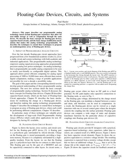
Input Capacitor<br />
poly2 cap<br />
<strong>Floating</strong> <strong>Gate</strong><br />
Transistor<br />
<strong>Floating</strong> <strong>Gate</strong><br />
Metal 1 Layer<br />
MOS Tunneling<br />
Capacitor<br />
I. IMPACT OF PROGRAMMABLE ANALOG CIRCUITS<br />
Over the last decade floating-gate circuit approaches have<br />
progressed from a few foundational academic results [1], [2] to<br />
a stable circuit <strong>and</strong> system technology with both academic <strong>and</strong><br />
industrial applications. This programmable analog technology<br />
empowers analog signal processing approaches programmable<br />
precision analog low-power techniques. An analog technology<br />
that is programmable can enable analog components to be seen<br />
as nearly user-friendly as configurable digital options. This<br />
approach allows power efficient computing for analog signal<br />
processing of 1000 to 10,000 times more efficient than custom<br />
digital computation, making a range of portable applications<br />
not possible for over a decade a possibility today.<br />
<strong>The</strong> goal of this paper <strong>and</strong> the corresponding tutorial session<br />
develop general underst<strong>and</strong>ing of these programmable analog<br />
techniques. <strong>The</strong> next few sections detail the basic concepts<br />
of programmable analog technology. Section II discusses the<br />
basic concepts for <strong>Floating</strong>-<strong>Gate</strong> devices. Chapter III describes<br />
capacitor-based circuits, which are the basis of <strong>Floating</strong>-<strong>Gate</strong><br />
Circuit approaches. Chapter IV describes the basic mechanisms<br />
for modifying the charge on a floating-gate device,<br />
<strong>and</strong> therefore making this analog technology programmable.<br />
Chapter V describes the techniques to extend these techniques<br />
to program an array of floating-gate devices, where each could<br />
be performing different computations. Chapter VI describes<br />
In particular, many of these techniques are valuable given<br />
the development of large-scale Field Programmable Analog<br />
Arrays (FPAAs) which could allow applications for non -IC<br />
designers by having ICs available..<br />
II. FLOATING-GATE CIRCUIT BASICS<br />
Figure 1a shows the layout, cross–section, <strong>and</strong> circuit symbol<br />
for the floating–gate pFET device [3]. A floating gate<br />
is a polysilicon gate surrounded by silicon–dioxide. Charge<br />
on the floating gate is stored permanently, providing a long–<br />
term memory, because it is completely surrounded by a high–<br />
quality insulator. From the layout, we see that the floating<br />
gate is a polysilicon layer that has no contacts to other layers.<br />
This floating gate can be the gate of a MOSFET <strong>and</strong> can<br />
be capacitively connected to other layers. In circuit terms, a<br />
V in<br />
SiO 2<br />
V s<br />
n-well<br />
SiO 2<br />
p-substrate<br />
V fg<br />
(<strong>Floating</strong> <strong>Gate</strong>)<br />
V d<br />
n-well<br />
p +<br />
n +<br />
V tun<br />
Fig. 1. Layout, cross section, <strong>and</strong> circuit diagram of the floating–gate pFET in<br />
a st<strong>and</strong>ard double–poly, n-well MOSIS process: <strong>The</strong> cross section corresponds<br />
to the horizontal line slicing through the layout view. <strong>The</strong> pFET transistor is<br />
the st<strong>and</strong>ard pFET transistor in the n-well process. <strong>The</strong> gate input capacitively<br />
couples to the floating–gate by either a poly–poly capacitor, a diffused linear<br />
capacitor, or a MOS capacitor, as seen in the circuit diagram (not explicitly<br />
shown in the other two figures). Between ÎØÙÒ <strong>and</strong> the floating–gate is our<br />
symbol for a tunneling junction—a capacitor with an added arrow designating<br />
the charge flow.<br />
floating gate occurs when we have no DC path to a fixed<br />
potential. No DC path implies only capacitive connections to<br />
the floating node, as seen in Fig. 1.<br />
<strong>The</strong> floating–gate voltage, determined by the charge stored<br />
on the floating gate, can modulate a channel between a source<br />
<strong>and</strong> drain, <strong>and</strong> therefore, can be used in computation. As<br />
a result, the floating-gate device can be viewed as a single<br />
transistor with one or several control gates where the designer<br />
controls the coupling into the surface potential. <strong>Floating</strong>–gate<br />
devices can compute a wide range of static <strong>and</strong> dynamic<br />
translinear functions by the particular choice of capacitive<br />
couplings into floating–gate devices [4].<br />
III. FLOATING-GATE CIRCUITS ENABLING CAPACITIVE<br />
CIRCUITS<br />
<strong>Floating</strong>–gate circuits provide IC designers with a practical,<br />
capacitor–based technology; since capacitors, rather than resistors,<br />
are a natural result of a MOS process. Figure 2 shows<br />
key basic capacitor circuit elements. Figure 2a shows the capacitive<br />
equivalent to a resistive voltage divider. <strong>The</strong> resulting<br />
expression is expected from a resistive voltage divider, except<br />
that we have an additional voltage, V Ö , that is set by the<br />
charge (Q) at the output node, as V Ö =Q/( ½ · ¾ ).<br />
Figure 2b shows the capacitor circuit for feedback around an<br />
Proceedings of the 9th International Database Engineering & Application Symposium (IDEAS’05)<br />
1098-8068/05 $20.00 © 2005 IEEE
V in<br />
C 1<br />
C 2<br />
V out<br />
V in<br />
C 1<br />
C 2<br />
= C eff<br />
/ G m<br />
SNR = 10 log 10<br />
(kT C eff<br />
)<br />
Linear Range =<br />
(C 1<br />
+ C 2<br />
+ C w<br />
)<br />
C 1<br />
<br />
<br />
<br />
<br />
<br />
<br />
<br />
<br />
<br />
<br />
<br />
C w<br />
G m<br />
V out<br />
C L<br />
C eff<br />
= (C 1 + C 2 + C w )(C 2 + C L ) - C 2 2<br />
(a)<br />
(c)<br />
C 2<br />
V in<br />
C 1<br />
C 2<br />
V out<br />
V 1<br />
C 2<br />
<br />
<br />
<br />
<br />
<br />
<br />
<br />
<br />
<br />
<br />
<br />
<br />
C 3<br />
S 1<br />
<br />
<br />
C sense<br />
<br />
<br />
<br />
<br />
<br />
<br />
<br />
<br />
<br />
<br />
<br />
<br />
<br />
<br />
<br />
<br />
<br />
(b)<br />
(d)<br />
V out<br />
Fig. 2. Basic capacitor circuits. In all cases, we have a charge term. (a) Capacitive Divider Circuit. (b) Capacitive Feedback around an amplifier. We<br />
assume the amplifier has MOS inputs; therefore inputs are practically only capacitive. (c) Assuming amplifier has a finite Gm, we identify the key parameters<br />
(b<strong>and</strong>width, SNR, <strong>and</strong> input linear range) for this amplifier (d) Circuit Modification for direct measurement of capacitive sensors.<br />
amplifier. As expected, the closed loop for this amplifier is<br />
½ ¾ ; the output of this amplifier also has a voltage term<br />
due to the charge stored (Q) at the ’-’ input terminal, where<br />
V Ö É ¾ .<br />
Figure 2c shows a more realistic circuit model for the<br />
amplifier circuit in 2b. This circuit description, which includes<br />
parasitic capacitances, is described as a single pole <strong>and</strong> zero<br />
system, assuming the amplifier sets a single pole (i.e. the<br />
amplifier has a frequency independent transconductance. In<br />
general, we describe the amplifier as a transconductance<br />
amplifier, assuming the gain set by the capacitors is lower<br />
than the amplifier gain. Increasing Û increases the input<br />
linear range; typically, Û is larger than ½ <strong>and</strong> ¾ , where<br />
Û models the input capacitance of the amplifier, explicitly<br />
drawn capacitance, <strong>and</strong> parasitic capacitances. Increasing the<br />
function Û Ä ¾ proportionately increases SNR (in signal<br />
power); therefore, unlike many filters where output noise <strong>and</strong><br />
SNR is set by the load capacitance (kT/C thermal noise), this<br />
function allows for lower drawn capacitances for a given noise<br />
floor. When we improve the linear range of this amplifier, we<br />
simultaneously improve the SNR of the amplifier. <strong>The</strong>se circuit<br />
approaches extend Transconductance-C filter approaches to<br />
allow some parameters to be set by the ratio of capacitors<br />
[5], such as b<strong>and</strong>pass gain, the linear range, the noise level,<br />
<strong>and</strong> b<strong>and</strong>width. <strong>The</strong>se approaches, coupled with the array<br />
programming discussions in Section IV, results in a highly<br />
accurate low-power filter technology.<br />
Figure 2d shows a slight extention of the other circuits<br />
towards measuring changes in capacitive sensors (i.e. MEMs<br />
sensors). Analyzing this circuit with an ideal amplifier with<br />
gain A Ú , we get<br />
¡ ×Ò×ÓÖ · ½<br />
´<br />
Î ÓÙØ Î Ú ×Ò×ÓÖ · Û µ<br />
½ <br />
¾<br />
¡Î ÓÙØ Î ½<br />
¡ ×Ò×ÓÖ<br />
¾<br />
(1)<br />
where C Û is the capacitance at the ’-’ amplifier input, including<br />
the amplifier input capacitance. This circuit configuration<br />
attenuates the effect of of sensor capacitance <strong>and</strong> C Û by the<br />
amplifier gain, an effect that is only a dc term assuming V ½<br />
remains constant. For example, for C ×Ò×ÓÖ = 1pF, maximum<br />
¡ ×Ò×ÓÖ = 2fF (typical of some MEMs sensors), <strong>and</strong> A Ú =<br />
1000, we choose C ¾ = 20fF for a maximum V ÓÙØ change of<br />
1V, resulting in an output offset voltage of 0.25V. <strong>The</strong> constant<br />
part of C ×Ò× , as well as C Û , increases the linear range of<br />
the closed-loop circuit.<br />
<strong>The</strong> dynamic performance of this amplifier is similar to<br />
techniques for Fig. 2. <strong>The</strong> circuit is still a first-order system<br />
(assuming a frequency independent amplifier Gm) described<br />
as<br />
Î ÓÙØ<br />
Î ½ ½ ×´ ¾ Ñ µ<br />
(2)<br />
¡ ×Ò×ÓÖ ¾ ½·×<br />
Proceedings of the 9th International Database Engineering & Application Symposium (IDEAS’05)<br />
1098-8068/05 $20.00 © 2005 IEEE
with the same timeconstant () as the amplifier in Fig. 2c, <strong>and</strong><br />
the zero, due to capacitive feedthrough, is typically at much<br />
higher frequency responses than the amplifier b<strong>and</strong>width.<br />
Typically, C ×Ò×ÓÖ <strong>and</strong> C Ä are roughly equal size (C Ä might<br />
be larger) <strong>and</strong> (the output load capacitance, as in Fig. 2c) are<br />
larger than C ¾ . For the example above, with Ä ×Ò×ÓÖ <br />
½Ô , the resulting b<strong>and</strong>width<br />
Transconductance ( Ñ ) Bias Current B<strong>and</strong>width<br />
1(kÅ) ½ 30A 3MHz (3)<br />
10 (kÅ) ½ 300A 30MHz<br />
<strong>The</strong> resulting output noise (entire b<strong>and</strong>) is<br />
Î ÓÙØ <br />
×ÕÎ Á Ò ´ ×Ò×ÓÖ · Û µ<br />
(4)<br />
¾ Ä<br />
where n is the equivalent number of devices contributing noise<br />
for the amplifier, <strong>and</strong> V Á is the ratio of the transconductance<br />
( Ñ ) <strong>and</strong> the differential pair transistor’s bias current. For the<br />
example above, with a typical low-noise amplifier stage with<br />
input transistors operating with subthreshold currents results<br />
in 0.5mV total noise, resulting in an SNR of roughly 66dB<br />
between the maximum capacitor deflection <strong>and</strong> the minimum<br />
deflection. For our example circuit, the maximum capacitance<br />
change of 2fF gives an output of 1V, where a 1aF change is at<br />
the 0dB SNR level; by restricting the b<strong>and</strong>width of interest or<br />
making the amplifier b<strong>and</strong>width larger than the b<strong>and</strong>width of<br />
interest, the resulting sensitivity will increase. In practice, we<br />
often allow for a bank of capacitors that can be switched into<br />
the circuit to alter C ¾ , <strong>and</strong> therefore the dynamic range <strong>and</strong><br />
noise of these signals. Figure 2d shows the switching between<br />
gain levels; the switch is not at the charge storage node because<br />
a MOS switch on the ’-’ terminal increases the leakage current<br />
at this node, decreasing hold time. All of these results have<br />
been experimentally verified through use of variable MEMs<br />
capacitor devices. In one particular system, one sees 100aF<br />
capacitor change resulting in 37.5mV change for an amplifier<br />
with noise significantly less than 1mV; therefore, 3fF change<br />
resulted in a 1.13V output swing, <strong>and</strong> 3aF change resulted in<br />
a 1mV output swing (0dB SNR point). <strong>The</strong> b<strong>and</strong>width of the<br />
amplifier was greater than 1MHz.<br />
IV. MODIFYING FLOATING-GATE CHARGE<br />
transistor I-V curve; therefore transistor elements<br />
We modify the floating–gate charge by applying large<br />
voltages across a silicon–oxide capacitor to tunnel electrons<br />
through the oxide or by adding electrons using hot–electron<br />
injection. Although we extensively discuss the physics of<br />
floating-gate circuits elsewhere [2], [6], [7], we briefly review<br />
the necessary physics below.<br />
A. Electron Tunneling<br />
We add charge to the floating gate by removing electrons<br />
using electron tunneling. Increasing the voltage across this<br />
tunneling capacitor, either by increasing the tunneling voltage<br />
(Î ØÙÒ ) or decreasing the floating-gate voltage, increases the<br />
effective electric field across the oxide, thereby increasing<br />
the probability of the electron tunneling through the barrier.<br />
Starting from the classic model of electron tunneling, given as<br />
Á ØÙÒ Á ¼ ´¼ØÓܵÎÓÜ (5)<br />
where ¼ is a fundamental parameter derived from a WKB<br />
solution of Schrodingers equation, I ¼ is an emperically measured<br />
parameter, t ÓÜ is the thickness of the oxide dielectric,<br />
<strong>and</strong> V ÓÜ is the voltage across the dielectric, we can derive an<br />
approximate model for the electron tunneling current around<br />
a given voltage acorss the oxide (tunneling voltage minus<br />
floating-gate voltage) as [2], [6]<br />
Á ØÙÒ Á ØÙÒ¼ ´ÎØÙÒ Î µÎ Ü<br />
(6)<br />
where Î Ü is a tunneling device-dependent parameter that is a<br />
function of the bias voltage across the oxide.<br />
V. PFET HOT-ELECTRON INJECTION<br />
We use pFET hot-electron injection to add electrons (remove<br />
charge) to the floating-gate. We use pFET hot-electron<br />
injection, because pFET hot-electron injection can not be<br />
eliminated from a CMOS process without adversely affecting<br />
basic transistor operation, <strong>and</strong> therefore will be available in all<br />
commercial CMOS processes. One might wonder how pFETs,<br />
where the current carriers are holes, inject hot electrons onto<br />
the floating gate. Figure 1b shows the b<strong>and</strong> diagram of a<br />
pFET operating under bias conditions that are favorable for<br />
hot-electron injection. <strong>The</strong> hot-hole impact ionization creates<br />
electrons at the drain edge of the drain-to-channel depletion<br />
region, due to the high electric fields there. <strong>The</strong>se electrons<br />
travel back into the channel region, gaining energy as they<br />
go. When their kinetic energy exceeds that of the silicon–<br />
silicon-dioxide barrier, they can be injected into the oxide <strong>and</strong><br />
transported to the floating gate. If we are to inject an electron<br />
onto a floating gate, the MOSFET must have a high-electricfield<br />
region ( ½¼V/Ñ ) to accelerate channel electrons to<br />
energies above the silicon–silicon-dioxide barrier, <strong>and</strong> in that<br />
region the oxide electric field must transport the electrons<br />
that surmount the barrier to the floating gate. As a result, the<br />
subthreshold MOSFET injection current is proportional to the<br />
source current, <strong>and</strong> is the exponential of a smooth function of<br />
the drain-to-channel potential (¨ ); the product of these two<br />
circuit variables is the key aspect necessary to build outerproduct<br />
learning rules. We present a first-principles model<br />
derived from basic physics that shows the resulting exponential<br />
functions elsewhere [8].<br />
A simplified model for pFET injection that is useful for<br />
h<strong>and</strong> calculations relates the hot-electron injection current for<br />
a channel current (I × ) <strong>and</strong> drain-to-source (¡Î × ) voltage as<br />
Á Ò Á Ò¼ « Á×<br />
¡Î ×Î Ò<br />
(7)<br />
Á ×¼<br />
where Á Ò¼ is the injection current when the pFET is operating<br />
with a channel current reference (Á ×¼ ), where Á × Á ×Ó at<br />
this reference current, <strong>and</strong> a drain-to-source voltage, Î Ò is<br />
a device <strong>and</strong> bias dependent parameter, <strong>and</strong> « is ½ ÍÌ<br />
Î Ò<br />
.<br />
Proceedings of the 9th International Database Engineering & Application Symposium (IDEAS’05)<br />
1098-8068/05 $20.00 © 2005 IEEE
V g<br />
V S V<br />
V fg<br />
V tun<br />
(a)<br />
V dd<br />
V tun<br />
V dd<br />
V tun<br />
V tun<br />
V 1 V 2<br />
C<br />
I 1 I<br />
C<br />
2<br />
<strong>Floating</strong>-gate<br />
(b)<br />
V tun<br />
well<br />
contact<br />
source<br />
(c)<br />
<strong>Floating</strong>-gate<br />
drain<br />
n-well<br />
<br />
p-substrate<br />
<br />
<br />
p-substrate<br />
n-well<br />
<br />
gate<br />
E c<br />
SiO 2<br />
<strong>Floating</strong><br />
<strong>Gate</strong><br />
E c<br />
V tun<br />
V ox<br />
V ox<br />
E c<br />
<strong>Floating</strong><br />
<strong>Gate</strong><br />
V ox<br />
V tun<br />
E c<br />
Channel<br />
<br />
<br />
Drain-to-Channel<br />
Depletion Region<br />
<br />
<br />
drain<br />
(d)<br />
(e)<br />
Fig. 3. Approach to modifying floating-gate charge. (a) Basic Circuit representation for a floating-gate device. (b) A programmable floating-gate differential<br />
pair. Both the input transistors as well as the current source transistor are programmed. Practically, we want to develop approaches to program the offset<br />
voltage for the amplifier, as well as the value for the current source. (c) Current–Voltage curves from a programmed pFET transistor. We modify charge<br />
by a complimentary combination of electron tunneling (weaker pFET transistor) <strong>and</strong> hot-electron injection (stronger pFET transistor). (d) Basic picture of<br />
electron tunneling in Si-SiO ¾ system (e) Basic picture of pFET hot-electron injection. Some holes moving through the channel gain sufficient energy to create<br />
an impact ionization event, generating electrons that increase in energy moving towards the channel. Some of these electrons will have sufficient energy to<br />
surmount the Si-SiO ¾ barrier <strong>and</strong> arrive at the gate terminal.<br />
Typical values for Î Ò in a 0.5m CMOS process are ½¼¼ÑÎ<br />
to ¾¼ÑÎ .<br />
Choosing the appropriate model for simulation is critical for<br />
these devices. For example, when simulating a set of floatinggate<br />
devices that will be programmed, one typically does not<br />
need to implement the tunneling <strong>and</strong> injection currents, but<br />
rather make sure at the beginning of the simulation that the<br />
floating-gate voltages / bias currents are set correctly based<br />
upon the behavior of the particular programming scheme. In<br />
this mode of operation, one can set the floating-gate voltage<br />
through a very large resistor; for the total capacitance at a<br />
floating-gate node of 100fF (a small device), a resistor of 10 ¾<br />
is consistent with the typical room temperature voltage drop<br />
of 4V over 10 year period for a 10nm oxide [9]. In some<br />
cases, transistor equivalent circuits can be used to simulate<br />
adaptive floating-gate elements, such as the C circuit <strong>and</strong> the<br />
ATS synapse element [5], [10]; these techniques tend to be<br />
useful circuits in their own right for applications requiring<br />
fast adaptation rates.<br />
VI. ACCURATE PROGRAMMING OF PROGRAMMABLE<br />
ANALOG<br />
<strong>The</strong> charge modification schemes, along with their detailed<br />
modeling, opens the door for accurate programming of a large<br />
number of floating-gate devices being utilized by a diverse set<br />
of circuits. Figure 4 shows the starting point for the story<br />
Proceedings of the 9th International Database Engineering & Application Symposium (IDEAS’05)<br />
1098-8068/05 $20.00 © 2005 IEEE
500<br />
V dd<br />
V dd<br />
V dd<br />
V dd<br />
Vdd<br />
I out<br />
Prog<br />
400<br />
V 1 V 2<br />
(a)<br />
Run<br />
V g<br />
Current (nA)<br />
300<br />
200<br />
V d<br />
Percentage Error (%)<br />
100<br />
0.7<br />
0.5<br />
0.3<br />
0.1<br />
0.1<br />
(b)<br />
0.3<br />
0 0 20 30 40 50 60 70<br />
<strong>Floating</strong>-<strong>Gate</strong> Position<br />
(c)<br />
Fig. 4. Programming of Large Number of <strong>Floating</strong>-<strong>Gate</strong> elements. (a) Infrastructure takes any number of floating-gate elements on a chip during run<br />
mode, <strong>and</strong> reconfigures these devices into a regular array of floating-gate elements. (b) Hot electron injection requires both channel current (subthreshold) <strong>and</strong><br />
high-electric field; therefore in an array of devices we can access a single element using an AND scheme, both for measurement <strong>and</strong> for programming. (c)<br />
Experimental measurements for programming a sequence of functions of different amplitudes. <strong>The</strong> corresponding percentage error is plotted below the data;<br />
the experimental error (for this example bounded between 0.7 percent <strong>and</strong> 0.3 percent) does not correlate with the experimental waveform.<br />
of automatically programming a large array of floating-gate<br />
elements. Figure 4a illustrates how we access programmable<br />
devices, which we define as Prog or program mode, <strong>and</strong> how<br />
we we compute using these elements, which we define as<br />
Run mode. When we go from Run mode to Prog mode, we<br />
electrically reconfigure all circuits such that each floating-gate<br />
device is configured into a two-dimensional mesh array of<br />
devices with the drain <strong>and</strong> gate lines moving in orthogonal<br />
directions. We isolate individual elements (access to an individual<br />
gate <strong>and</strong> drain line) in a large matrix using peripheral<br />
control circuitry [3], [7]. A st<strong>and</strong>ard technique is necessary<br />
when working with thous<strong>and</strong>s <strong>and</strong> millions of floating-gate<br />
elements on a single die.<br />
Our programming scheme minimizes interaction between<br />
floating–gate devices in an array during the programming<br />
operation. Other elements are switched to a separate voltage to<br />
ensure that those devices will not inject. We program a device<br />
by increasing the output current using hot-electron injection,<br />
<strong>and</strong> erase a device by decreasing the output current using<br />
electron tunnelling. Because of the poorer selectivity, we use<br />
tunnelling primarily for erasing <strong>and</strong> for rough programming<br />
steps. Our programming scheme performs injection over a<br />
fixed time window (from 1s to 10s <strong>and</strong> larger) using drainto-source<br />
voltage based on the actual <strong>and</strong> target currents.<br />
Most rapid programming techniques use pulse widths in the<br />
10s to 100s range. which potentially enable programming<br />
large arrays of floating-gate elements in mass production.<br />
Developing an efficient algorithm for pFET programming<br />
requires discussing the dependencies of the gate currents as<br />
a function of the drain-to-source voltage. This scheme also<br />
measures results at the circuit’s operating condition for optimal<br />
tuning of the operating circuit (no compensation circuitry<br />
needed). Once programmed, the floating-gate devices retain<br />
their channel current in a non-volatile manner. We designed<br />
a custom programming board (PCB board) to program large<br />
floating-gate arrays around these st<strong>and</strong>ards [7], [11], <strong>and</strong> have<br />
been developing approaches to move all of these blocks onchip<br />
using row-parallel programming techniques [12]. <strong>The</strong>se<br />
approaches have been used by over 40 researchers on hundreds<br />
of IC projects. <strong>The</strong> limiting factor for rapid programming<br />
of these devices is the speed <strong>and</strong> accuracy of our current<br />
measurements; the hot-electron injection physics does not limit<br />
the speed of the programming with current approaches.<br />
Often, one is asked how accurately can these devices be<br />
programmed. In the end, the accuracy is limited by change in<br />
voltage (¡Î ) due to one electron (Õ) moving off of the total<br />
capacitance ( Ì ) at the floating node, expressed as<br />
¡Î Õ Ì (8)<br />
Proceedings of the 9th International Database Engineering & Application Symposium (IDEAS’05)<br />
1098-8068/05 $20.00 © 2005 IEEE
For C Ì of 16fF (a small device), the voltage change from<br />
one electron is 10V. For a voltage source based on the<br />
floating-gate voltage for a 2V swing, the accuracy is roughly<br />
0.0005 percent or 17 - 18 bits. For a subthreshold current<br />
source, the accuracy is roughly 0.05 percent (11 bit) over the<br />
entire subthreshold current range (typically 6 to 8 orders of<br />
magnitude). <strong>The</strong> error decreases inversely proportional to an<br />
increasing C Ì .<br />
<strong>The</strong>refore, the real question is how accurately can the<br />
programming algorithm achieve this theoretical limit. First,<br />
the limitation is the accuracy of measuring the quantity we<br />
desire to program; for example, if we only have 8bit accuracy<br />
to measure the output current we want to program, then we can<br />
not expect to achieve significantly higher programming performance<br />
through that measurement. Second, is the limitation of<br />
the programming algorithm <strong>and</strong> associated circuitry, including<br />
parasitic elements; our approaches are designed to minimizes<br />
the effect of parasitic elements by design. On the other h<strong>and</strong>,<br />
due to factors like capacitor mismatch, we can usually have<br />
fine-tuning programming steps to improve the effects due to<br />
these mismatches. [5], [13] Finally, C Ì can set the thermal<br />
noise (kT/C noise) for the previous stage; a 16fF capacitor will<br />
set a total noise for a single subthreshold device as 0.25mV,<br />
an error if not addressed in the resulting circuit, will be 25<br />
times greater than the programming accuracy. Figure 4c shows<br />
measurements of programming accuracy from an array of<br />
floating-gate devices ( C Ì ½¼¼fF). Typical experimental<br />
results show that we can program within 0.5 to 0.1 percent<br />
accuracy over 3.5 decades of target currents, we can program<br />
at least as well as 1 percent accuracy over 6 decodes of target<br />
currents, in CMOS processes ranging from 0.5m to 0.25m<br />
CMOS processes [14].<br />
[6] P. Hasler, B. A. Minch, <strong>and</strong> C. Diorio, “Adaptive circuits using pFET<br />
floating-gate devices,” in Proceedings of the 20th Anniversary Conference<br />
on Advanced Research in VLSI, Atlanta, GA, March 1999, pp.<br />
215–229.<br />
[7] M. Kucic, P. Hasler, J. Dugger, <strong>and</strong> D. V. Anderson, “Programmable<br />
<strong>and</strong> adaptive analog filters using arrays of floating-gate circuits,” in 2001<br />
Conference on Advanced Research in VLSI, E. Brunv<strong>and</strong> <strong>and</strong> C. Myers,<br />
Eds. IEEE Computer Society, March 2001, pp. 148–162.<br />
[8] C. Duffy <strong>and</strong> P. Hasler, “Modeling hot-electron injection in pfet’s,”<br />
Journal of Computational Electronics, vol. 2, pp. 317–322, Jan. 2001.<br />
[9] V. Srinivasan, G. J. Serrano, J. Gray, <strong>and</strong> P. Hasler, “A precision<br />
cmos amplifier using floating-gates for offset cancellation,” in Custom<br />
Integrated <strong>Circuits</strong> Conference, San Jose, Sept. 2005.<br />
[10] V. Srinivasan, J. Dugger, <strong>and</strong> P. Hasler, “An adaptive analog synapse<br />
circuit that implements the least-mean-square learning algorithm,” in<br />
Proceedings of the International Symposium on <strong>Circuits</strong> <strong>and</strong> <strong>Systems</strong>,<br />
Kobe, Japan, May 2005.<br />
[11] G. Serrano, P. Smith, H. Lo, R. Chawla, T. Hall, C. Twigg, <strong>and</strong><br />
P.Hasler, “Automatic rapid programming of large arrays of floating-gate<br />
elements,” in Proceedings of the International Symposium on <strong>Circuits</strong><br />
<strong>and</strong> <strong>Systems</strong>, Vancouver, May 2004.<br />
[12] M. Kucic, Ed., Analog Computing Arrays. Atlanta, GA: Ph.D.<br />
Dissertation, Georgia Institute of Technology, 2004.<br />
[13] A. B<strong>and</strong>yopadhyay, J. Lee, R. Robucci, <strong>and</strong> P. Hasler, “A 80uw/frame<br />
104x128 cmos imager front-end for jpeg compression,” in Proceedings<br />
of the International Symposium on <strong>Circuits</strong> <strong>and</strong> <strong>Systems</strong>, Kobe, Japan,<br />
May 2005.<br />
[14] A. B<strong>and</strong>yopadhyay, G. Serrano, <strong>and</strong> P. Hasler, “Programming analog<br />
computational memory elements to 0.2 percent accuracy over 3.5<br />
decades of current,” in Proceedings of the International Symposium on<br />
<strong>Circuits</strong> <strong>and</strong> <strong>Systems</strong>, Kobe, Japan, May 2005.<br />
VII. ACKNOWLEDGEMENTS<br />
This paper has been heavily based upon the research in the<br />
CADSP laboratory at Georgia Tech, founded by David Anderson<br />
<strong>and</strong> myself. In particular, I greatly appreciate the many<br />
discussions with graduate students that have helped shape the<br />
focus of this paper: Farhan Adil, Abhishek B<strong>and</strong>yopadyady,<br />
Ravi Chawla, Chris Duffy, Jeff Dugger, David Graham, Jordan<br />
Gray, Tyson Hall, Matt Kucic, Guillermo Serrano, Paul Smith,<br />
Venkatesh Srinivasan. <strong>and</strong> Chris Twigg.<br />
REFERENCES<br />
[1] T. Shibata <strong>and</strong> T. Ohmi, “A functional MOS transistor featuring gatelevel<br />
weighted sum <strong>and</strong> threshold operations,” IEEE Transactions on<br />
Electron <strong>Devices</strong>, vol. 39, no. 6, pp. 1444–1455, 1992.<br />
[2] P. Hasler, C. Diorio, B. A. Minch, <strong>and</strong> C. A. Mead, Advances in Neural<br />
Information Processing <strong>Systems</strong> 7. Cambridge, MA: MIT Press, 1995,<br />
ch. Single transistor learning synapses, pp. 817–824.<br />
[3] P. Hasler <strong>and</strong> T. S. L<strong>and</strong>e, “Special issue on floating-gate devices,<br />
circuits, <strong>and</strong> systems,” IEEE Journal of <strong>Circuits</strong> <strong>and</strong> <strong>Systems</strong>, vol. 48,<br />
no. 1, Jan. 2001.<br />
[4] B. A. Minch, P. Hasler, <strong>and</strong> C. Diorio, “Multiple-input translinear<br />
element networks,” IEEE Transactions on <strong>Circuits</strong> <strong>and</strong> <strong>Systems</strong> II,<br />
vol. 48, no. 1, pp. 20–28, Jan. 2001.<br />
[5] D. Graham, P. D. Smith, R. Ellis, R. Chawla, <strong>and</strong> P. Hasler, “Programmable<br />
b<strong>and</strong>pass array using floating-gate elements,” in Proceedings<br />
of the International Symposium on <strong>Circuits</strong> <strong>and</strong> <strong>Systems</strong>, Vancouver, BC,<br />
May 2004.<br />
Proceedings of the 9th International Database Engineering & Application Symposium (IDEAS’05)<br />
1098-8068/05 $20.00 © 2005 IEEE