Lab Manual v1.2013 - Cristinel Ababei
Lab Manual v1.2013 - Cristinel Ababei
Lab Manual v1.2013 - Cristinel Ababei

Create successful ePaper yourself
Turn your PDF publications into a flip-book with our unique Google optimized e-Paper software.
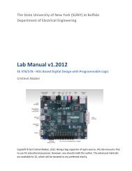
The State University of New York (SUNY) at Buffalo<br />
Department of Electrical Engineering<br />
<strong>Lab</strong> <strong>Manual</strong> <strong>v1.2013</strong><br />
EE 379/578 – Embedded Systems and Applications<br />
<strong>Cristinel</strong> <strong>Ababei</strong><br />
Copyleft © by <strong>Cristinel</strong> <strong>Ababei</strong>, 2013. Being a big supporter of open-source, this lab manual is free<br />
to use for educational purposes. However, you should credit the author. The advanced materials<br />
are available for $1, which will be donated to my preferred charity.
Table of Contents<br />
<strong>Lab</strong> 1: A “Blinky” Introduction to C and Assembly Programming .................................................................... 3<br />
<strong>Lab</strong> 2: Using UART .......................................................................................................................................... 13<br />
<strong>Lab</strong> 3: Debugging and More on Interrupts ..................................................................................................... 23<br />
<strong>Lab</strong> 4: CAN and I2C ......................................................................................................................................... 32<br />
<strong>Lab</strong> 5: USB audio, Stepper Motor .................................................................................................................. 47<br />
<strong>Lab</strong> 5: Supplemental Material – SPI and SD cards ......................................................................................... 54<br />
<strong>Lab</strong> 6: Introduction to RTX Real-Time Operating System (RTOS) .................................................................. 66<br />
<strong>Lab</strong> 7: Introduction to Ethernet ..................................................................................................................... 74<br />
<strong>Lab</strong> 7: Supplemental Material – AR.Drone Control........................................................................................ 91<br />
<strong>Lab</strong> 8: Streaming Video from CMOS Camera ................................................................................................. 98<br />
Notes on Using MCB1700 Board .................................................................................................................... 99<br />
2
<strong>Lab</strong> 1: A “Blinky” Introduction to C and Assembly Programming<br />
1. Objective<br />
The objective of this lab is to give you a “first foot in the door” exposure to the programming in C and<br />
assembly of a program, which when executed by the microcontroller (NXP LPC1768, an ARM Cortex-M3)<br />
simply blinks LEDs located on the development board. You also learn how to use the ARM Keil uVision<br />
IDE to create projects, build and download them to the board (either Keil MCB1700 or Embest EM-<br />
LPC1700).<br />
2. Pre-lab Preparation<br />
Optional (but encouraged)<br />
You should plan to work on your own computer at home a lot during this semester. You should install the<br />
main software (evaluation version) we will use in this course: the Microcontroller Development Kit (MDK-<br />
ARM), which supports software development for and debugging of ARM7, ARM9, Cortex-M, and Cortex-R4<br />
processor-based devices. Download it from ARM’s website [1] and install it on your own computer. This is<br />
already installed on the computers in the lab.<br />
MDK combines the ARM RealView compilation tools with the Keil µVision Integrated Development<br />
Environment (IDE). The Keil µVision IDE includes: Project Management and Device & Tool<br />
Configuration, Source Code Editor Optimized for Embedded Systems, Target Debugging and Flash<br />
Programming, Accurate Device Simulation (CPU and Peripheral).<br />
You should read this lab entirely before attending your lab session. Equally important, you should/browse<br />
related documents suggested throughout the description of this lab. These documents and pointers are<br />
included either in the downloadable archive for this lab or in the list of References. Please allocate<br />
significant amount of time for doing this.<br />
3. <strong>Lab</strong> Description<br />
a. BLINKY 1<br />
Creating a new project<br />
1. First create a new folder called say EE378_S2013 where you plan to work on the labs of this course.<br />
Then, inside it, create a new folder called lab1.<br />
2. Launch uVision4, Start->All Programs->Keil uVision4<br />
3. Select Project->New uVision Project… and then select lab1 as the folder to save in; also type blinky1<br />
as the File Name.<br />
4. Then, select NXP (founded by Philips) LPC1768 as CPU inside the window that pops-up. Also, click<br />
Yes to Copy “startup_LPCxx.s” to Project Folder.<br />
5. Under File Menu select New.<br />
6. Write your code in the and save it as blinky1.c in the same project folder. This file (as well as all others<br />
discussed in this lab) is included in the downloadable archive from the website of this course. The panel<br />
on the left side of the uVision IDE is the Project window. The Project window gives you the hierarchy<br />
of Target folder and Source Group folder.<br />
3
7. Right click on the “Source Group 1” and select “Add files to Source Code”.<br />
8. Locate blinky1.c and include it to the group folder.<br />
9. Copy C:\Keil\ARM\Startup\NXP\LPC17xx\system_LPC17xx.c to lab1 directory and add it as a<br />
source file to the project too. Open this file and browse it quickly to see what functions are defined<br />
inside it.<br />
10. Click Project menu and then select Build Target.<br />
11. Build Output panel should now show that the program is being compiled and linked. This creates<br />
blinky1.axf file (in ARM Executable Format), which will be downloaded to the board. To create a .hex<br />
file (more popular), select Flash->Configure Flash Tools->Output and check mark Create HEX File.<br />
12. Connect the board to two USB ports of the host computer. One connection is to the port J16 of the<br />
board (the one that is a Standard-B plug). The second connection is via the ULINK2<br />
debugger/programmer/emulator. These connections are illustrated in Fig.1.<br />
13. Download the program to the Flash of the microcontroller. Select Flash->Download. This loads the<br />
blinky1.axf file. Then press the RESET push-button of the board.<br />
14. Congratulations! You just programmed your first project. You should notice that the LED P1.29 is<br />
blinking. If this is not the case, then you should investigate/debug your project to make it work.<br />
Figure 1 Connection of ULINK2 to the board.<br />
Debugging<br />
If your program has errors (discovered by compiler or linker) or you simply want to debug it to verify its<br />
operation, then we can use the debugging capabilities of the uVision tools.<br />
1. Click Debug menu option and select Start/Stop Debug Session. A warning about the fact that this is an<br />
evaluation version shows up; click OK.<br />
2. Then, a new window appears where we can see the simulation of the program.<br />
3. This window has several different supportive panels/sub-windows where we can monitor changes<br />
during the simulation. The left hand side panel, Registers, provides information regarding the Registers<br />
of LPC17xx with which we are working.<br />
4. Again, click on the Debug menu option and select Run. The code starts simulating.<br />
5. It is good practice that before going ahead with the actual hardware implementation to perform a<br />
debug/simulation session to make sure that our program behaves according to the design requirements.<br />
6. In our example, we use PORT1.<br />
4
7. Go to Peripherals menu option then select GPIO Fast Interface followed by Port 1.<br />
8. You should get the window shown in Fig.2 below, where you can see LED P1.29 blinking. To actually<br />
observe this you should wait until the simulated time (shown on the bottom-right side of the uVision<br />
ISE window) is longer than 1 second. Note that in order to actually simulate 1 second of execution time<br />
of the program, the simulator must run much longer. This is expected, as typically simulators require<br />
much longer computational runtimes (wallclock time) in order to simulate relatively short execution<br />
times of the program under investigation!<br />
9. This is a standard method to check that your program works correctly.<br />
10. The debugger is a very powerful tool. This is only a brief exposure to it; we’ll revisit it many times later<br />
in this course. Once you are done with the simulation/debug of your program, you can stop it by<br />
selecting Start/Stop the Debug Session from the Debug menu option. This stops the show and takes us<br />
back to the main uVision window.<br />
Figure 2 Pin P1.29 is checked on/off every other second or so.<br />
Taking it further<br />
At this time, you should revisit blinky1.c file. Read this file (it has lots of comments) and browse<br />
related/included files in order to fully understand what is what and what it does. This is very important.<br />
You should take time to read/browse on your own the user’s guide of the board, the user manual and<br />
datasheet of LPC17xx microcontrollers as well as other files included in the downloadable archive of this<br />
lab [2-5]. Do not attempt to print them as some have >800 pages.<br />
Note that because it is very difficult to cover everything during the lectures and labs, you are expected to<br />
proactively engage materials related to this course and take ownership of your learning experience! This<br />
is a necessary (but not sufficient) attitude to do well in this course.<br />
b. BLINKY 2<br />
Start uVision and select Project->Open Project, then, browse to open the Blinky project example located at:<br />
C:\Keil460\ARM\Boards\Keil\MCB1700\Blinky<br />
As you noticed, the ARM Kiel software installation contains a folder called Boards that contains design<br />
examples for a variety of boards. We’ll use some of these design examples for the board utilized in this<br />
course. However, as we go, you should take a look and play with all these examples; try to understand their<br />
code.<br />
Build the project and download to target. Observe operation and comment.<br />
5
At this time, you should take time to read the .c files of this project, starting with Blinky.c. Read it and also<br />
browse the other files to gain insights into what and how the code achieves different tasks. At this stage, do<br />
not expect to understand everything; however, please make an effort to see as much as you can.<br />
c. BLINKY 3<br />
In this part of the lab, we implement the blinky example by writing a program in assembly language. In this<br />
example we’ll turn on/off the LED controlled by pin P1.28. Start uVision and create a new project. Add to<br />
it the following files:<br />
1. When creating the project say Yes to have added startup_LPCxx.s to the project<br />
2. blinky3.s (available in the downloadable archive of this lab as well in an ppendix at the end of this lab)<br />
3. C:\Keil\ARM\Startup\NXP\LPC17xx\system_LPC17xx.c. This is needed for the SystemInit()<br />
function called from within startup_LPCxx.s. We could not add this file to the project provided that<br />
we comment out the two lines inside startup_LPCxx.s that contain SystemInit.<br />
Build the project and download to target. Observe operation and comment.<br />
At this time, you should take time to read the blinky3.s. Read it and make sure you understand how the<br />
code achieves each task.<br />
4. <strong>Lab</strong> Assignment<br />
Modify the assembly program blinky3.s to implement the following design description: blink all eight<br />
LEDs on the board, one by one from left to right repeatedly.<br />
For each lab with a “<strong>Lab</strong> Assignment”, you must turn-in a lab report in PDF format (font size 11, single<br />
spacing), named lab#_firstname_lastname.pdf (where “#” is the number of the lab, for example in the<br />
case of lab1, “#” must be replaced with 1) which should contain the following sections:<br />
<strong>Lab</strong> title, Your name<br />
Introduction section – a brief description of the problem you solve in this lab assignment, outlining the<br />
goal and design requirements.<br />
Solution section – describe the main technique(s) that you utilized to develop your solution. Include<br />
block diagrams, flow graphs, plots, etc. here to aid your explanation.<br />
Results and Conclusion section – describe your results and any issues you may have faced during the<br />
assignment and how you solved them.<br />
Code listings, assembly or C code that you wrote. Appended at the end of your report. Use smaller font<br />
(size 9) to save space.<br />
For full credit, you must demo the correct operation of your assignment to the TA during the next lab.<br />
While you are free to hand-write your report (still turned-in as a PDF file), please make sure your report is<br />
neat and the presentation is coherent. You will lose points for reports that do not present enough details, are<br />
ugly, disorganized, or are hard to follow/read.<br />
5. Credits and references<br />
[1] Software: Microcontroller Development Kit; download from http://www.keil.com/arm/mdk.asp<br />
6
[2] Hardware: MCB1700 board User’s Guide;<br />
http://www.keil.com/support/man/docs/mcb1700/mcb1700_su_connecting.htm<br />
[3] LPC17xx user’s manual; http://www.nxp.com/documents/user_manual/UM10360.pdf<br />
[4] NXP LPC17xx datasheet;<br />
http://www.nxp.com/documents/data_sheet/LPC1769_68_67_66_65_64_63.pdf<br />
http://www.keil.com/dd/chip/4868.htm<br />
[5] Cortex-M3 information;<br />
http://www.nxp.com/products/microcontrollers/cortex_m3/<br />
http://www.arm.com/products/processors/cortex-m/cortex-m3.php<br />
[6] Additional resources<br />
--Keil uVision User’s Guide<br />
http://www.keil.com/support/man/docs/uv4/<br />
-- Keil uVision4 IDE Getting Started Guide<br />
www.keil.com/product/brochures/uv4.pdf<br />
--ARM Assembler Guide<br />
http://www.keil.com/support/man/docs/armasm/<br />
--ARM Compiler toolchain for uVision. Particularly browse:<br />
ARM Compiler toolchain for uVision, Using the Assembler<br />
ARM Compiler toolchain for µVision, Using the Linker<br />
http://infocenter.arm.com/help/index.jsp?topic=/com.arm.doc.dui0377c/index.html<br />
--Professor J.W. Valvano (UTexas) resources;<br />
http://users.ece.utexas.edu/~valvano/Volume1/uvision/<br />
--UWaterloo ECE254, Keil MCB1700 Hardware Programming Notes<br />
https://ece.uwaterloo.ca/~yqhuang/labs/ece254/doc/MCB1700_Hardware.pdf<br />
----EE 472 Course Note Pack, Univ. of Washington, 2009,<br />
http://abstract.cs.washington.edu/~shwetak/classes/ee472/notes/472_note_pack.pdf (Chapter 6)<br />
APPENDIX A: Some info on LPC1768 peripherals programming<br />
Pins on LPC1768 are divided into 5 ports indexed from 0 to 4. Pin naming convention is Px.y, where x is<br />
the port number and y is the pin number. For example, P1.29 means Port 1, Pin 29. Each pin has four<br />
operating modes: GPIO (default), first alternate function, second alternate function, and third alternate<br />
function. Any pin of ports 0 and 2 can be used to generate an interrupt.<br />
To use any of the LPC1768 peripherals, the general steps to be followed are:<br />
1. Power Up the peripheral to be used<br />
2. Set the Clock Rate for the peripheral<br />
3. Specify the pin operating mode - Connect necessary pins using Pin Connect Block<br />
4. Set direction - Initialize the registers of the peripheral<br />
1. Power Up the peripheral<br />
Let’s assume we are interested in utilizing the pin P1.29 to drive one of the board’s LEDs on and off<br />
(the blinky1 example). Refer to LPC17xx User’s <strong>Manual</strong>, Chapter 4: Clocking and Power Control.<br />
Look for register Power Control for Peripherals register, PCONP. It’s on page 63; bit 15 is PGPIO.<br />
Setting this bit to 1 should power up the GPIO ports. Note that the default value is 1 anyway, which<br />
7
means GPIO ports are powered up by default on reset; but the start up code may modify this. Hence,<br />
it’s good practice to make sure we take care of it. For example, here is how we power up the GPIO:<br />
LPC_SC->PCONP |= 1 PINSEL3 &= ~((3
We turn a pin to HIGH/LOW (i.e., digital logic 1/0) by setting the corresponding bit in<br />
FIOSET/FIOCLR register. Both FIOSET and FIOCLR are member variables defined in the<br />
PC_GPIO_TypeDef C struct. To set a pin to digital 1, set the corresponding bit of LPC_GPIOx-<br />
>FIOSET to 1. To turn a pin to digital 0, set the corresponding bit of LPC_GPIOx->FIOCLR to 1.<br />
Refer to Sections 9.5.2 and 9.5.3 of LPC17xx User’s manual for details.<br />
For example, to turn on LED P1.29, the following code can be used:<br />
LPC_GPIO1->FIOSET = 1 FIOSET = mask;<br />
}<br />
Of course, to turn off a particular LED, just replace FIOSET with FIOCLR in the above code.<br />
Note: we can also set HIGH/LOW a particular output pin via the FIOPIN register. We can write<br />
specific bits of the FIOPIN register to set the corresponding pin to the desired logic value. In this<br />
way, we bypass the need to use both the FIOSET and FIOCLR registers. However, this is not the<br />
recommended method. For example, in the case of the blinky example, we use the following C code:<br />
LPC_GPIO1->FIOPIN |= 1 FIOPIN &= ~( 1 FIOPIN value to obtain pin value(s). Refer to Section 9.5.4 in the<br />
LPC17xx User’s manual for details. For example, to read the joystick position, the following code<br />
can be used<br />
#define KBD_MASK 0x79<br />
uint32_t kbd_val;<br />
kbd_val = (LPC_GPIO1->FIOPIN >> 20) & KBD_MASK;<br />
When the joystick buttons are inactive, the bits located at P1.23,24,25,26 are logic 1. When any of<br />
the joystick buttons becomes active, the bit corresponding to that pin becomes 0.<br />
APPENDIX B: Listing of blinky3.s<br />
; CopyLeft (:-) <strong>Cristinel</strong> <strong>Ababei</strong>, SUNY at Buffalo, 2012<br />
; this is one assembly implementation of the infamous blinky example;<br />
9
; target microcontroler: LPC1768 available on board Keil MCB1700 (or Embest EM-LPC1700 board)<br />
; I tested it first on EM-LPC1700 board as it's cheaper!<br />
;<br />
; Note1: it has lots of comments, as it is intended for the one who<br />
; sees for the first time assembly;<br />
; Note2: some parts of the implementation are written in a more complicated manner<br />
; than necessary for the purpose of illustrating for example different memory<br />
; addressing methods;<br />
; Note3: each project will have to have added to it also system_LPC17xx.s (added<br />
; automatically by Keil uVision when you create your project) and system_LPC17xx.c<br />
; which you can copy from your install directory of Keil IDE (for example,<br />
; C:\Keil\ARM\Startup\NXP\LPC17xx\system_LPC17xx.c)<br />
; Note4: system_LPC17xx.s basically should contain the following elements:<br />
; -- defines the size of the stack<br />
; -- defines the size of the heap<br />
; -- defines the reset vector and all interrupt vectors<br />
; -- the reset handler that jumps to your code<br />
; -- default interrupt service routines that do nothing<br />
; -- defines some functions for enabling and disabling interrupts<br />
; Directives<br />
; they assist and control the assembly process; directives or "pseudo-ops"<br />
; are not part of the instruction set; they change the way the code is assembled;<br />
; THUMB directive placed at the top of the file to specify that<br />
; code is generated with Thumb instructions;<br />
THUMB<br />
; some directives define where and how the objects (code and variables) are<br />
; placed in memory; here is a list with some examples:<br />
; AREA, in assembly code, the smallest locatable unit is an AREA<br />
; CODE is the place for machine instructions (typically flash ROM)<br />
; DATA is the place for global variables (typically RAM)<br />
; STACK is the place for the stack (also in RAM)<br />
; ALIGN=n modifier starts the area aligned to 2^n bytes<br />
; |.text| is used to connect this program with the C code generated by<br />
; the compiler, which we need if linking assembly code to C code;<br />
; it is also needed for code sections associated with the C library;<br />
; NONINT defines a RAM area that is not initialized (normally RAM areas are<br />
; initialized to zero); Note: ROM begins at 0x00000000 and RAM begins at<br />
; 0x2000000;<br />
; EXPORT is a directive in a file where we define an object and<br />
; IMPORT directive is used in a file from where we wish to access the object;<br />
; Note: we can export a function in an assembly file and call the function<br />
; from a C file; also, we can define a function in C file, and IMPORT the function<br />
; into an assembly file;<br />
; GLOBAL is a synonym for EXPORT<br />
; ALIGN directive is used to ensure the next object is aligned properly; for example,<br />
; machine instructions must be half-word aligned, 32-bit data accessed with LDR, STR<br />
; must be word-aligned; good programmers place an ALIGN at the end of each file so the<br />
; start of every file is automatically aligned;<br />
; END directive is placed at the end of each file<br />
; EQU directive gives a symbolic name to a numeric constant, a register-relative<br />
; value or a program-relative value; we'll use EQU to define I/O port addresses;<br />
AREA |.text|, CODE, READONLY ; following lines are to be placed in code space<br />
EXPORT __main<br />
ENTRY<br />
10
; EQUates to make the code more readable; to turn LED P1.28 on and off<br />
; we will write the bit 28 of the registers FIO1SET (to set HIGH) and FIO1CLR (to set LOW);<br />
; refer to page 122 of the LPC17xx user manual to see the adresses of these registers; they are:<br />
FIO1SET EQU 0x2009C038<br />
FIO1CLR EQU 0x2009C03C<br />
; we will implement a dirty delay by decrementing a large enough<br />
; number of times a register;<br />
LEDDELAY EQU 10000000<br />
__main<br />
; (1) we want to set as output the direction of the pins that<br />
; drive the 8 LEDs; these pins belong to the ports Port 1 and Port 2<br />
; and are: P1.28, P1,29, P1.31 and P2.2,...,6<br />
; to set them as output, we must set to 1 the corresponding bits in<br />
; registers (page 122 of LPC17xx user manual):<br />
; FIO1DIR - 0x2009C020<br />
; FIO2DIR - 0x2009C040<br />
; that is, we'll set to 1 bits 28,29,31 of the register at adress 0x2009C020,<br />
; which means writing 0xB0000000 to this location; also, we'll set 1 bits 2,...,6<br />
; of the register at address 0x2009C040, which means writing 0x0000007C to<br />
; this location;<br />
MOV R1, #0x0 ; init R1 register to 0 to "build" address<br />
MOVT R1, #0x2009 ; assign 0x20090000 to R1; MOVT assigns to upper nibble<br />
MOV R3, #0xC000 ; move 0xC000 into R3<br />
ADD R1, R1, R3 ; add 0xC000 to R1 to get 0x2009C000<br />
MOV R4, #0xB0000000 ; place 0xB0000000 (i.e., bits 28,29,31) into R4<br />
; now, place contents of R4 (i.e. 0xB0000000) to address<br />
; 0x2009C020 (i.e., register FIO1DIR); this sets pins<br />
; 28,29,31 as output direction;<br />
; Note: address is created by adding the offset 0x20 to R1<br />
; Note: the entire complication above could be replaced with<br />
; simply loading R1 with =FIO1DIR (but we wanted to experiment with<br />
; different flavors of MOV, to upper and lower nibbles); we'll use<br />
; the simpler version later;<br />
STR R4, [R1, #0x20]<br />
MOV R4, #0x0000007C ; value to go to register of Port 2<br />
STR R4, [R1, #0x40] ; set output direction for pins of Port 2 by writing to reister FIO2DIR<br />
; (2) set HIGH the LED driven by P1.28; to do that we load current<br />
; contents of register FIO1SET (i.e., memory address 0x2009C038) to R3,<br />
; set to 1 its 28th bit, and then put it back into the location at<br />
; memory address 0x2009C038 (i.e., effectively writing into register FIO1SET);<br />
LDR R1, =FIO1SET ; we'll not touch R1 anymore so that it keeps this address<br />
LDR R3, [R1]<br />
ORR R3, #0x10000000 ; set to logic 1 bit 28 of R3<br />
STR R3, [R1]<br />
; (3) some initializations<br />
LDR R0, =LEDDELAY ; initialize R0 for countdown<br />
LDR R2, =FIO1CLR ; we'll not touch R2 anymore so that it keeps this address<br />
; now, the main thing: turn the LED P1.28 on and off repeatedly;<br />
; this is done by setting the bit 28 of registers FIO1CLR and FIO1SET;<br />
; Note: one could do this in a simpler way by using a toggling trick:<br />
; toggle (could be done using exclusive or with 1) bit 28 of register<br />
; FIO1PIN instead (page 122 of LPC17xx user manual) and not use<br />
; FIO1CLR and FIO1SET; I do not recommend however this trick as<br />
11
loop<br />
led_on<br />
led_off<br />
; due to the peculiarities of FIO1PIN;<br />
SUBS R0, #1 ; decrement R0; this sets N,Z,V,C status bits<br />
BNE led_on ; if zero not reached yet, go back and keep decrementing<br />
LDR R3, [R2] ; recall that R2 stores =FIO1CLR<br />
ORR R3, #0x10000000 ; set to logic 1 bit 28 of R3<br />
STR R3, [R2] ; place R3 contents into FIO1CLR, which will put pin on LOW<br />
LDR R0, =LEDDELAY ; initialize R0 for countdown<br />
SUBS R0, #1 ; decrement R0; this sets N,Z,V,C status bits<br />
BNE led_off ; if zero not reached yet, go back and keep decrementing<br />
LDR R3, [R1] ; recall that R1 stores =FIO1SET<br />
ORR R3, #0x10000000 ; set to logic 1 bit 28 of R3<br />
STR R3, [R1] ; place R3 contents into FIO1SET, which will put pin on HIGH<br />
LDR R0, =LEDDELAY ; initialize R0 for countdown<br />
; now do it again;<br />
B loop<br />
ALIGN<br />
END<br />
12
<strong>Lab</strong> 2: Using UART<br />
1. Objective<br />
The objective of this lab is to utilize the Universal Asynchronous Receiver/Transmitter (UART) to connect<br />
the MCB1700 board to the host computer. Also, we introduce the concept of interrupts briefly. In the<br />
example project, we send characters to the microcontroller unit (MCU) of the board by pressing keys on the<br />
keyboard. These characters are sent back (i.e., echoed, looped-back) to the host computer by the MCU and<br />
are displayed in a hyperterminal window.<br />
2. UART<br />
The most basic method for communication with an embedded processor is asynchronous serial. It is<br />
implemented over a symmetric pair of wires connecting two devices (referred as host and target here,<br />
though these terms are arbitrary). Whenever the host has data to send to the target, it does so by sending an<br />
encoded bit stream over its transmit (TX) wire. This data is received by the target over its receive (RX)<br />
wire. The communication is similar in the opposite direction. This simple arrangement is illustrated in<br />
Fig.1. This mode of communications is called “asynchronous” because the host and target share no time<br />
reference (no clock signal). Instead, temporal properties are encoded in the bit stream by the transmitter and<br />
must be decoded by the receiver.<br />
Figure 1 Basic serial communication.<br />
A commonly used device for encoding and decoding such asynchronous bit streams is a Universal<br />
Asynchronous Receiver/Transmitter (UART). UART is a circuit that sends parallel data through a serial<br />
line. UARTs are frequently used in conjunction with the RS-232 standard (or specification), which specifies<br />
the electrical, mechanical, functional, and procedural characteristics of two data communication equipment.<br />
A UART includes a transmitter and a receiver. The transmitter is essentially a special shift register that<br />
loads data in parallel and then shifts it out bit by bit at a specific rate. The receiver, on the other hand, shifts<br />
in data bit by bit and reassembles the data. The serial line is ‘1’ when it is idle. The transmission starts with<br />
a start-bit, which is ‘0’, followed by data-bits and an optional parity-bit, and ends with stop-bits, which are<br />
‘1’. The number of data-bits can be 6, 7, or 8. The optional parity bit is used for error detection. For odd<br />
parity, it is set to ‘0’ when the data bits have an odd number of ‘1’s. For even parity, it is set to ‘0’ when the<br />
data-bits have an even number of ‘1’s. The number of stop-bits can be 1, 1.5, or 2. The transmission with 8<br />
data-bits, no parity, and 1 stop-bit is shown in Fig.2 (note that the LSB of the data word is transmitted first).<br />
Figure 2 Transmission of a byte.<br />
13
No clock information is conveyed through the serial line. Before the transmission starts, the transmitter and<br />
receiver must agree on a set of parameters in advance, which include the baud-rate (i.e., number of bits per<br />
second), the number of data bits and stop bits, and use of parity bit.<br />
To understand how the UART's receiver extracts encoded data, assume it has a clock running at a multiple<br />
of the baud rate (e.g., 16x). Starting in the idle state (as shown in Fig.3), the receiver “samples” its RX<br />
signal until it detects a high-low transition. Then, it waits 1.5 bit periods (24 clock periods) to sample its RX<br />
signal at what it estimates to be the center of data bit 0. The receiver then samples RX at bit-period intervals<br />
(16 clock periods) until it has read the remaining 7 data bits and the stop bit. From that point this process is<br />
repeated. Successful extraction of the data from a frame requires that, over 10.5 bit periods, the drift of the<br />
receiver clock relative to the transmitter clock be less than 0.5 periods in order to correctly detect the stop<br />
bit.<br />
Figure 3 Illustration of signal decoding.<br />
UARTs can be used to interface to a wide variety of other peripherals. For example, widely available<br />
GSM/GPRS cell phone modems and Bluetooth modems can be interfaced to a microcontroller UART.<br />
Similarly GPS receivers frequently support UART interfaces.<br />
The NXP LPC1768 microcontroller includes four such devices/peripherals called UARTs: UART0/2/3 and<br />
UART1. See pages 298 and 318 of the LPC17xx User’s <strong>Manual</strong> [1]. See also page 27 of the Datasheet [2].<br />
UART0 and UART1 of the microcontroller are connected on the MCB1700 board to the ST3232C (IC6),<br />
which converts the logic signals to RS-232 voltage levels. This connection is realized from pins<br />
{P0.2/TXD0/AD0.7 and P0.3/RXD0/AD0.6} and { P2.0/PWM1.1/TXD1 and P2.1/PWM1.2/RXD1} of the<br />
microcontroller to the pins {10, 9, 11, and 12} ST3232C chip. The ST3232C chip drives the two COM0<br />
and COM1 represented by the two female DB9 connectors (Note: if you use an Embest LPC1700 board,<br />
then, note that these two connectors are male DB9 connectors). To see these connections, take a look on<br />
pages 1 and 3 of the schematic diagram of the board [3] (included also in the downloadable files of this<br />
lab#2).<br />
For more details on UART and RS-232, please read references [1-6].<br />
In this lab we will explore serial communication between the (target) LPC1768 UART and a serial<br />
communication port of the host PC.<br />
3. EXAMPLE 1: Microcontroller “echoes” back the characters sent by host computer<br />
(a) Experiment<br />
In the first example of this lab, we’ll use an example project that comes with the “LPC1700 code bundle”.<br />
The LPC1700 Code Bundle is a free software package from NXP that demonstrates the use of the built-in<br />
peripherals on the NXP LPC17xx series of microcontrollers. The example software includes a common<br />
library, peripheral APIs, and test modules for the APIs.<br />
14
Download LPC1700 Code Bundle from [7] (http://ics.nxp.com/support/software/code.bundle.lpc17xx.keil/)<br />
and save it in your own work directory. Save it with the plan to keep it as we’ll revisit some other example<br />
in the future. Unzip it to get the keil_examples folder created with several examples therein. Take a minute<br />
and read keil_example/readme.txt now.<br />
Launch Keil uVision4 and then open the project UART from among the example just downloaded. The<br />
UART project is a simple program for the NXP LPC17xx microcontrollers using Keil’s MCB1700<br />
evaluation board. When sending some characters from a terminal program on the PC at a speed of 57600<br />
Baud to the LPC17xx UART0 or UART1 the LPC17xx will echo those same characters back to the<br />
terminal program.<br />
Step 1: Connect the board, ULINK2, and the host computer as shown in Fig.4. Ask the TA for the COM0/1<br />
to Serial Port cable.<br />
Figure 4 Hardware setup.<br />
Remove the RST and ISP jumpers. Please keep the jumpers safe and place them back when you are done<br />
with this lab.<br />
Note: If you are doing this lab using a laptop which does not have a serial port, you can use a USB Serial<br />
Converter. I got mine for about $12 from Amazon [8] and it works great.<br />
Step 2: Familiarize yourself with the following files:<br />
--uart.c: contains the UART0 / UART1 handlers / driver functions<br />
--uarttest.c: contains a small test program utilizing the UART driver<br />
--system_LPC17xx.c: Cortex-M3 Device Peripheral Access Layer Source File<br />
--startup_LPC17xx.s: CMSIS Cortex-M3 Core Device Startup File<br />
--Abstract.txt: Describes what the uarttest.c program does<br />
Change "#include "lpc17xx.h" to "#include . This is done in order to use the latest Keil’s<br />
release of the header file (normally located in C:\Keil\ARM\INC\NXP directory).<br />
Step 3: Make sure the uVision4 Target setting is FLASH. Then, build the project by rebuilding all target<br />
files. Download to the microcontroller and confirm that download is ok.<br />
Step 4: Establish a Terminal connection<br />
--Method 1: If your Windows is XP or older, you can use HyperTerminal:<br />
15
--Start HyperTerminal by clicking Start - > All Programs -> Accessories -> Communications -><br />
HyperTerminal<br />
--Connect HyperTerminal to the serial port that is connected to the COM0 port of the evaluation board for<br />
example. For the HyperTerminal settings you should use: COM1 (double check that it the host’s serial port<br />
is indeed COM1in your case – you can do that by Start->Control Panel->System->Hardware->Device<br />
Manager and click on Ports (COM & LPT); if in your case it’s a different port number then use that; for<br />
example, in my case as I use the USB to serial adapter with my laptop, the port is COM14), baud rate<br />
57600, 8 data bits, no parity, 1 stop bit, and no flow control.<br />
--Method 2: If your Windows is 7 or newer, you first must make sure you download and/or install a serial<br />
connection interface (because HyperTerminal is not part of Windows 7 or later). On the machines in the<br />
lab, you can use Putty (http://www.putty.org):<br />
--Start->All Programs->Putty->Putty<br />
--Then, select Connection, Serial and type COM1 (or whatever is in your case; find what it is as described<br />
in Method 1), baud rate 57600, 8 data bits, no parity, 1 stop bit, and no flow control.<br />
--Click on Session and choose the type of connection as Serial. Save the session for example as "lab2".<br />
--Finally, click on Open; you should get HyperTerminal like window.<br />
--Method 3: You can use other programs such as:<br />
TeraTerm (http://logmett.com/index.php?/products/teraterm.html) or<br />
HyperSerialPort (http://www.hyperserialport.com/index.html) or<br />
RealTerm (http://realterm.sourceforge.net) or CoolTerm (http://freeware.the-meiers.org), etc.<br />
Step 5: Type some text. It should appear in the HyperTerminal window. This is the result of: First, what<br />
you type is sent to the microcontroller via the serial port (that uses a UART). Second, the MCU receives<br />
that via its own UART and echoes (sends back) the typed characters using the same UART. The host PC<br />
receives the echoed characters that are displayed in the HyperTerminal.<br />
Disconnect the serial cable from COM0 and connect it to COM1 port on the MCB1700 board. The behavior<br />
of project should be the same.<br />
Step 6: (optional – do not do it on computers in the lab): On your own computer only, download and install<br />
NXP’s FlashMagic tool from here:<br />
http://www.flashmagictool.com/<br />
Then, follow the steps that describe how to use this tool as presented in the last part of the UART<br />
documentation for the code bundle:<br />
http://ics.nxp.com/literature/presentations/microcontrollers/pdf/code.bundle.lpc17xx.keil.uart.pdf (included<br />
in the downloadable archive of files for this lab).<br />
Note: With this approach one does not need the ULINK2 programmer/debugger.<br />
(b) Brief program description<br />
Looking at the main() function inside the uarttest.c file we can see the following main actions:<br />
--UART0 and UART1 are initialized:<br />
UARTInit(0, 57600); /* baud rate setting */<br />
UARTInit(1, 57600); /* baud rate setting */<br />
--A while loop which executes indefinitely either for UART0 or for UART1. The instructions executed<br />
inside this loop (let’s assume the UART0) are:<br />
16
Disable Receiver Buffer Register (RBR), which contains the next received character to be read. This is<br />
achieved by setting all bits of the Interrupt Enable Register (IER) to ‘0’ except bits THRE and RLS. In<br />
this way the LSB (i.e., bit index 0 out of 32 bits) of IER register is set to ‘0’. The role of this bit (as<br />
explained in the LPC17xx User’s <strong>Manual</strong> [1] on page 302) when set to ‘0’ is to disable the Receive<br />
Data Available interrupt for UART0.<br />
Send back to the host the characters from the buffer UART0Buffer. This is done only if there are<br />
characters in the buffer (the total buffer size is 40 characters) which have been received so far from the<br />
host PC. The number of characters received so far and not yet echoed back is stored and updated in<br />
UART0Count.<br />
Once the transmission of all characters from the buffer is done, reset the counter UART0Count.<br />
Enable Receiver Buffer Register (RBR). This is achieved by setting to ‘1’ the LSB of IER, which in<br />
turn is achieved using the mask IER_RBR.<br />
(c) Source code discussion<br />
Please take your time now to thoroughly browse the source code in files uart.c and uarttest.c files. Open<br />
and read other files as necessary to track the declarations and descriptions of variables and functions.<br />
For example, in uarttest.c we see:<br />
--A function call SystemClockUpdate();<br />
This is described in source file system_LPC17xx.c which we locate in the Project panel of the uVision4<br />
IDE. Click on the name of this file to open and search inside it the description of SystemClockUpdate().<br />
This function is declared in header file system_LPC17xx.h. Open these files and try to understand how this<br />
function is implemented; what each of the source code lines do?<br />
--A function call UARTInit(0, 57600);<br />
This function is described in source file uart.c. The declaration of this function is done inside header file<br />
uart.h. Open these files and read the whole code; try to understand each line of the code.<br />
--An instruction:<br />
LPC_UART0->IER = IER_THRE | IER_RLS; /* Disable RBR */<br />
Based on what’s been studied in lab#1 you should know already that LPC_UART0 is an address of a<br />
memory location – the UART0 peripheral is “mapped” to this memory location. Starting with this memory<br />
location, several consecutive memory locations represent “registers” associated with this peripheral/device<br />
called UART0. All 14 such registers (or memory locations) are listed on page 300 of the User <strong>Manual</strong>.<br />
Utilizing this peripheral is done through reading/writing into these registers according to their meaning and<br />
rules described in the manual. For example, one of the 14 registers associated with UART0 is Interrupt<br />
Enable Register (IER).<br />
Form a C programming perspective, LPC_UART0 is declared inside header file LPC17xx.h:<br />
#define LPC_UART0 ((LPC_UART_TypeDef *) LPC_UART0_BASE )<br />
Which also declares what LPC_UART0_BASE as:<br />
#define LPC_UART0_BASE (LPC_APB0_BASE + 0x0C000)<br />
Where LPC_APB0_BASE is declared at its turn in the same file:<br />
#define LPC_APB0_BASE<br />
(0x40000000UL)<br />
This effectively makes LPC_UART0_BASE to have value: 0x4000C000, which not surprisingly coincides<br />
with what is reported on page 14 of the LPC17xx User’s <strong>Manual</strong>!<br />
Furthermore, the Interrupt Enable Register (IER) contains individual interrupt enable bits for the 7 potential<br />
UART interrupts. The IER register for UART0 is “mapped” (or associated with) to memory address<br />
17
0x4000C004 as seen on page 300 of the LPC17xx User’s <strong>Manual</strong>. This fact is captured in the struct<br />
declaration of LPC_UART_TypeDef inside the header file LPC17xx.h (open this file and double check<br />
it!). As a result, in our C programming, we can refer to the IER register as in the instruction that we are<br />
currently discussing: LPC_UART0->IER, which basically stores/represents the address 0x4000C004.<br />
In addition, note that IER_THRE and IER_RLS are declared inside the header file uart.h as:<br />
#define IER_THRE 0x02<br />
#define IER_RLS 0x04<br />
Which are utilized as masks in our instruction:<br />
LPC_UART0->IER = IER_THRE | IER_RLS; /* Disable RBR */<br />
So, finally as we see, the effect of this instruction is simply to turn ‘1’ bit index 1 (the second LSB out of 32<br />
bits) and bit index 2 (the third LSB out of 32 bits) of the IER register! All other bits are set to ‘0’.<br />
Having bit index 1 of this register set to ‘1’ enables the Transmit Holding Register Empty (THRE) flag for<br />
UART0 – see page 302, Table 275 of the LPC17xx User’s <strong>Manual</strong>. Having bit index 2 of this register set to<br />
‘1’ enables the UART0 RX line status interrupts – see page 302, Table 275 of the LPC17xx User’s <strong>Manual</strong>.<br />
As already said, all other bits are set therefore via this masking to ‘0’. This includes the LSB (i.e., bit index<br />
0 out of 32 bits) of IER register, which is set to ‘0’. The role of this bit (as explained in the LPC17xx User’s<br />
<strong>Manual</strong> on page 302) when set to ‘0’ is to disable the Receive Data Available interrupt for UART0.<br />
You should be able now to explain what the following instruction does:<br />
LPC_UART0->IER = IER_THRE | IER_RLS | IER_RBR; /* Re-enable RBR */<br />
Summarizing, what the code inside uarttest.c does is (as also mentioned in the previous section):<br />
--disable receiving data<br />
--send back data to the PC from the buffer (i.e., array variable UART0Buffer)<br />
--reset counter of characters stored in buffer<br />
--enable receiving data<br />
Note: As mentioned in lab#1, in general one would not need to worry about these details about addresses to<br />
which registers are mapped. It would be sufficient to just know of for example the definition and declaration<br />
of LPC_UART_TypeDef inside the header file LPC17xx.h. To the C programmer, it is transparent to what<br />
exact address the register IER is mapped to for example. However, now at the beginning, it’s instructive to<br />
track these things so that we get a better global picture of these concepts. It also forces us to get better used<br />
with the LPC17xx User’s <strong>Manual</strong> and the datasheets.<br />
Notice that inside the source file uart.c we have these two function descriptions:<br />
void UART0_IRQHandler (void) {...}<br />
void UART1_IRQHandler (void) {...}<br />
which are not called for example inside uarttest.c, but they appear inside startup_LPC17xx.s:<br />
DCD UART0_IRQHandler ; 21: UART0<br />
DCD UART1_IRQHandler ; 22: UART1<br />
The function void UART0_IRQHandler (void) is the UART0 interrupt handler. Its name is<br />
UART0_IRQHandler because it is named like that by the startup code inside the file startup_LPC17xx.s.<br />
DCD is an assembler directive (or pseudo-op) that defines a 32-bit constant.<br />
To get a better idea about these things, we need to make a parenthesis and discuss a bit about interrupts in<br />
the next section. For the time being this discussion is enough. We will discuss interrupts in more details in<br />
class lectures and in some of the next labs as well.<br />
18
----------------------------------------------------------------------------------------------------------------------------------<br />
(d) Interrupts – a 1 st encounter<br />
An interrupt is the automatic transfer of software execution in response to a hardware event that is<br />
asynchronous with the current software execution. This hardware event is called a trigger. The hardware<br />
event can either be a busy to ready transition in an external I/O device (i.e., peripheral, like for example the<br />
UART input/output) or an internal event (like bus fault, memory fault, or a periodic timer). When the<br />
hardware needs service, signified by a busy to ready state transition, it will request an interrupt by setting its<br />
trigger flag.<br />
A thread is defined as the path of action of software as it executes. The execution of the interrupt service<br />
routine (ISR) is called as a background thread, which is created by the hardware interrupt request and is<br />
killed when the ISR returns from interrupt (e.g., by executing a BX LR in an assembly program). A new<br />
thread is created for each interrupt request. In a multi-threaded system, threads are normally cooperating to<br />
perform an overall task. Consequently, we’ll develop ways for threads to communicate (e.g., FIFOs) and<br />
synchronize with each other.<br />
A process is also defined as the action of software as it executes. Processes do not necessarily cooperate<br />
towards a common shared goal. Threads share access to I/O devices, system resources, and global variables,<br />
while processes have separate global variables and system resources. Processes do not share I/O devices.<br />
To arm (disarm) a device/peripheral means to enable (shut off) the source of interrupts. Each potential<br />
interrupting trigger has a separate “arm” bit. One arms (disarms) a trigger if one is (is not) interested in<br />
interrupts from this source.<br />
To enable (disable) means to allow interrupts at this time (postponing interrupts until a later time). On the<br />
ARM Coretx-M3 processor, there is one interrupt enable bit for the entire interrupt system. In particular, to<br />
disable interrupts we set the interrupt mask bit, I, in PRIMASK register.<br />
Note: An interrupt is one of five mechanisms to synchronize a microcontroller with an I/O device. The<br />
other mechanisms are blind cycle, busy wait, periodic polling, and direct memory access. With an input<br />
device, the hardware will request an interrupt when input device has new data. The software interrupt<br />
service will read from the input device and save in global RAM. With an output device, the hardware will<br />
request an interrupt when the output device is idle. The software interrupt service will get data from a<br />
global structure, and write it to the device. Sometimes, we configure the hardware timer to request<br />
interrupts on a periodic basis. The software interrupt service will perform a special function; for example, a<br />
data acquisition system needs to read the ADC at a regular rate.<br />
On the ARM Cortex-M3 processor, exceptions include resets, software interrupts, and hardware<br />
interrupts. Each exception has an associated 32-bit vector that points to the memory location where the<br />
ISR that handles the exception is located. Vectors are stored in ROM at the beginning of the memory. Here<br />
is an example of a few vectors as defined inside startup_LPC17xx.s:<br />
__Vectors<br />
DCD __initial_sp ; Top of Stack<br />
DCD Reset_Handler ; Reset Handler<br />
DCD NMI_Handler ; NMI Handler<br />
DCD HardFault_Handler ; Hard Fault Handler<br />
...<br />
19
; External Interrupts<br />
DCD WDT_IRQHandler ; 16: Watchdog Timer<br />
DCD TIMER0_IRQHandler ; 17: Timer0<br />
...<br />
DCD UART0_IRQHandler ; 21: UART0<br />
...<br />
ROM location 0x00000000 has the initial stack pointer and location 0x00000004 contains the initial<br />
program counter (PC), which is called the reset vector. It points to a function called reset handler, which is<br />
the first thing executed following reset.<br />
Interrupts on the Cortex-M3 are controlled by the Nested Vector Interrupt Controller (NVIC). To activate<br />
an “interrupt source” we need to set its priority and enable that source in the NVIC (i.e., activate =<br />
set priority + enable source in NVIC). This activation is in addition to the “arm” and “enable” steps<br />
discussed earlier.<br />
Table 50 in the User <strong>Manual</strong> (page 73) lists the interrupt sources for each peripheral function. Table 51<br />
(page 76 in User <strong>Manual</strong>) summarizes the registers in the NVIC as implemented in the LPC17xx<br />
microcontroller. Read the entire Chapter 6 of the User <strong>Manual</strong> (pages 72-90) and identify the priority and<br />
enable registers and their fields of the NVIC. Pay particular attention to (i.e., search/watch for) UART0 in<br />
this Chapter. How would you set the priority and enable UART0 as a source of interrupts?<br />
----------------------------------------------------------------------------------------------------------------------------------<br />
Coming back to our discussion of the function void UART0_IRQHandler (void) in uart.c, we see a first<br />
instruction:<br />
IIRValue = LPC_UART0->IIR;<br />
What does it do? It simply reads the value of LPC_UART0->IIR and assigns it to a variable whose name<br />
is IIRValue. LPC_UART0->IIR is the value of the register IIR (Interrupt IDentification Register -<br />
identifies which interrupt(s) are pending), which is one of several (14 of them) registers associated with the<br />
UART0 peripheral/device. You can see it as well as the other registers on page 300 of the User <strong>Manual</strong>.<br />
Take a while and read them all. The fields of the interrupt register IIR are later described on page 303 in the<br />
User <strong>Manual</strong>. Take another while and read them all on pages 303-304.<br />
Next inside uart.c we see:<br />
IIRValue >>= 1; /* skip pending bit in IIR */<br />
IIRValue &= 0x07; /* check bit 1~3, interrupt identification */<br />
Which shifts right with one bit IIRValue and then AND’s it with 0x07. This effectively “zooms-in” onto the<br />
field formed by bits index 1-3 from the original LPC_UART0->IIR, bits which are now in the position bits<br />
index 0-2 of IIRValue variable.<br />
Going on, we find an “if” instruction with several branches:<br />
if ( IIRValue == IIR_RLS ) /* Receive Line Status */<br />
{...<br />
}<br />
else if ( IIRValue == IIR_RDA ) /* Receive Data Available */<br />
{...<br />
}<br />
else if ( IIRValue == IIR_CTI ) /* Character timeout indicator */<br />
{...<br />
}<br />
else if ( IIRValue == IIR_THRE ) /* THRE, transmit holding register empty */<br />
20
{...<br />
}<br />
See in Table 276 on page 303 in the User <strong>Manual</strong> what is the meaning of the three bits 1-3 from the original<br />
IIR register:<br />
011 1 - Receive Line Status (RLS).<br />
010 2a - Receive Data Available (RDA).<br />
110 2b - Character Time-out Indicator (CTI).<br />
001 3 - THRE Interrupt<br />
For each of these situations, something else is done inside the corresponding branch of the “if” instruction<br />
above. In other words, we first identify the interrupt, and for each ID we do something else. If none of the<br />
expected IDs is found, we do nothing. Please take your time now to explain what’s done in each of these<br />
cases. Read pages 303-304 in the User <strong>Manual</strong> for this. This is very important in order to understand the<br />
overall operation of the example of this lab.<br />
4. <strong>Lab</strong> Assignment<br />
1) (not graded and should not be discussed in the lab report) Use a Debug session to step through the<br />
execution of this program. The scope is for you to better understand its operation. See lab#1 for how to<br />
use/run a debug session. See also documentation of the code bundle from NXP [7].<br />
2) Answer the question: Why did we need to remove the ISP and RST jumpers in Example 1?<br />
3) Describe in less than a page (typed, font size 11, single line spacing) all instructions inside the function<br />
void UART0_IRQHandler (void) for each of the branches of the main “if” instruction. Include this in your<br />
lab report.<br />
4) Modify Example 1 such that the characters typed on the host’s keyboard are also displayed on the LCD<br />
display on the board. (Hint: re-use code from Blinky2 example of lab#1)<br />
5. Credits and references<br />
[1] LPC17xx user’s manual; http://www.nxp.com/documents/user_manual/UM10360.pdf (part of lab#1<br />
files)<br />
[2] NXP LPC17xx Datasheet;<br />
http://www.nxp.com/documents/data_sheet/LPC1769_68_67_66_65_64_63.pdf (part of lab#1 files)<br />
[3] Schematic Diagram of the MCB1700 board; http://www.keil.com/mcb1700/mcb1700-schematics.pdf<br />
(part of lab#2 files)<br />
[4] MCB1700 Serial Ports; http://www.keil.com/support/man/docs/mcb1700/mcb1700_to_serial.htm<br />
[5] UART entry on Wikipedia (click also on the references therein for RS-232);<br />
http://en.wikipedia.org/wiki/Universal_asynchronous_receiver/transmitter<br />
[6]<br />
--Jonathan W. Valvano, Embedded Systems: Introduction to Arm Cortex-M3 Microcontrollers, 2012.<br />
(Chapters 8,9)<br />
--Pong P. Chu, FPGA Prototyping by VHDL Examples: Xilinx Spartan-3 Version, Wiley 2008. (Chapter 7)<br />
--<strong>Lab</strong> manual of course http://homes.soic.indiana.edu/geobrown/c335 (Chapter 5)<br />
--EE 472 Course Note Pack, Univ. of Washington, 2009,<br />
http://abstract.cs.washington.edu/~shwetak/classes/ee472/notes/472_note_pack.pdf (Chapter 8)<br />
[7] LPC1700 Code Bundle;<br />
Download: http://ics.nxp.com/support/software/code.bundle.lpc17xx.keil/<br />
21
Documentation:<br />
http://ics.nxp.com/literature/presentations/microcontrollers/pdf/code.bundle.lpc17xx.keil.uart.pdf<br />
[8] Pluggable USB to RS-232 DB9 Serial Adapter;<br />
Amazon: http://www.amazon.com/Plugable-Adapter-Prolific-PL2303HX-<br />
Chipset/dp/B00425S1H8/ref=sr_1_1?ie=UTF8&qid=1359988639&sr=8-<br />
1&keywords=plugable+usb+to+serial<br />
Tigerdirect: http://www.tigerdirect.com/applications/SearchTools/itemdetails.asp?EdpNo=3753055&CatId=464<br />
22
<strong>Lab</strong> 3: Debugging and More on Interrupts<br />
1. Objective<br />
The objective of this lab is to learn about the different features of the debugger of uVision. We’ll do this by<br />
experimenting with several examples. We’ll also re-emphasize some aspects about interrupts (UART and<br />
Timer) via these examples.<br />
2. uVision Debuger<br />
The μVision Debugger is completely integrated into the μVision IDE. It provides many features, including<br />
the following [1]:<br />
--Disassembly of the code on C/C++ source- or assembly-level with program execution in various stepping<br />
modes and various view modes, like assembler, text, or mixed mode<br />
--Multiple breakpoint options including access and complex breakpoints<br />
--Review and modify memory, variable, and register values<br />
--List the program call tree including stack variables<br />
--Review the status of on-chip microcontroller peripherals<br />
--Debugging commands or C-like scripting functions<br />
--Code Coverage statistics for safety-critical application testing<br />
--Various analyzing tools to view statistics, record values of variables and peripheral I/O signals, and to<br />
display them on a time axis<br />
--Instruction Trace capabilities to view the history of executed instructions<br />
The μVision Debugger offers two operating modes:<br />
1) Simulator Mode - configures the μVision Debugger as a software-only product that accurately<br />
simulates target systems including instructions and most on-chip peripherals (serial port, external I/O,<br />
timers, and interrupts; peripheral simulation capabilities vary depending on the device you have<br />
selected.). In this mode, you can test your application code before any hardware is available. It gives<br />
you serious benefits for rapid development of reliable embedded software.<br />
2) Target Mode - connects the μVision Debugger to real hardware. Several target drivers are available<br />
that interface to a:<br />
-ULINK JTAG/OCDS Adapter that connects to on-chip debugging systems<br />
-Monitor that may be integrated with user hardware or that is available on many evaluation boards<br />
-Emulator that connects to the microcontroller pins of the target hardware<br />
-In-System Debugger that is part of the user application program and provides basic test functions<br />
-ULINKPro Adapter a high-speed debug and trace unit connecting to on-chip debugging systems via<br />
JTAG/SWD/SWV, and offering Cortex-M3ETM Instruction Trace capabilities<br />
Debug Menu<br />
The Debug Menu of uVision IDE includes commands that start and stop a debug session, reset the CPU,<br />
run and halt the program, and single-step in high-level and assembly code. In addition, commands are<br />
available to manage breakpoints, view RTOS Kernel information, and invoke execution profiling. You can<br />
modify the memory map and manage debugger functions and settings.<br />
23
Debug Toolbar<br />
Take a moment and read pages 67-68 of the uV IDE Getting Started Guide [1]. The discussion on these<br />
pages present all the icons of the IDE related to the debugger.<br />
Pre-lab preparation<br />
Please take some time now and read fully Chapters 7,8,9 from the uV IDE Getting Started Guide [1].<br />
3. Example 1 – Blinky 1 Revisited<br />
The files necessary for this example are located in example1 folder as part of the downloadable archive for<br />
this lab. As mentioned earlier, the μVision Debugger can be configured as a Simulator or as a Target<br />
Debugger. In this example, we’ll use the Simulator. Go to the Debug tab of the Options for Target dialog to<br />
switch between the two debug modes and to configure each mode. Configure to Use Simulator. Before<br />
running the simulation, replace the following two lines inside blinky1.c:<br />
delay( 1 FIOPIN |= 1 FIOPIN &= ~( 1
3. Debug->Run. Notice that the simulation starts and runs till the first breakpoint where it stops. Notice<br />
that P1.29 is 0. To continue the simulation click the icon “Step (F11)” once. What happens? P1.29 is<br />
turned 1 and we stepped with the simulation to the next instruction inside our program.<br />
4. Step (F11) again more times. Observe what happens each time. While stepping inside the delay()<br />
function, observe the value of local variable “i” inside the panel labeled Call Stack + Locals on the<br />
bottom right side of the uVision IDE. Notice how “i” is incremented. To get out from within the delay()<br />
function click the icon “Step out (Ctrl-F11)”.<br />
5. Once you get a hang of it, stop the simulation.<br />
Logic Analyzer<br />
The debugger includes a logic analyzer that will allow you to study the relative timing of various signals<br />
and variable changes. It’s activated using the button in the debugger. Note that you can only use the logic<br />
analyzer when you’re running in the simulator, not on the board.<br />
The logic analyzer is mostly self-explanatory. Use the Setup button to add channels. You can use symbolic<br />
names such as FIO1PIN to determine what registers or variables to watch, and you can specify a mask value<br />
(which is ANDed with the contents of the register or variable) and a right shift value (which is applied after<br />
the AND operation). You can view the result as a numeric value (“analog”) or as a bit value. At any point<br />
you can stop the updating of the screen (and/or stop the simulation itself), and change the resolution to<br />
zoom in or out. You can also scroll forward and backward in time using the scrollbar below the logic<br />
analyzer window. There are also “prev” and “next” buttons to move quickly from one transition to another.<br />
1. Open the Logic Analyzer by clicking the icon Analysis Windows->Logic Analyzer<br />
2. Click Setup… in the new window of the logic analyzer. Then, click New (Insert) icon and type<br />
FIO1PIN. Type in 0x20000000 as “And Mask”.<br />
3. Go to Peripherals menu option then select GPIO Fast Interface followed by Port 1 to show the GPIO1<br />
Fast Interface.<br />
4. Run simulation and observe how the signal changes inside the Logic Analyzer window.<br />
4. Example 2 – UART1 sends “Hello World! “ Once Only<br />
The files necessary for this example are located in example2 folder as part of the downloadable archive for<br />
this lab. This example is a modified (simplified) version of the example from lab#2. The simplified version<br />
uses only UART1 to simply send to the PC the string of characters “Hello World! “.<br />
Please take a moment and read the new files uart.h, uart.c, and uarttest.c. Observe the differences<br />
compared to the original example from lab#2. Discuss with your team member the functionality of this new<br />
example.<br />
To work with this example, go to your own folder where you have saved keil_examples/ (this is the codebundle<br />
of lab#2) and copy the whole directory UART/ to UART_modified/. Then, replace the files uart.h,<br />
uart.c, and uarttest.c from UART_modified/ with the ones provided in folder example2 of the<br />
downloadable archive of this lab. We make this copy and work inside keil_examples/ to avoid copying files<br />
from keil_examples/common/ (such as type.h).<br />
Launch uVision and open the project from UART_modified/. Build the project and download to the board<br />
as you did in lab#2. Use a Putty terminal (or a HyperTerminal if you use Windows XP) to see that indeed<br />
“Hello World! “ is printed out.<br />
25
Simulation Debug<br />
1. Configure the debugger to Use Simulator.<br />
2. Click Debug menu option and select Start/Stop Debug Session.<br />
3. Select View->Serial Windows->UART #2. In this window we can see what is sent out from UART1.<br />
4. Select View->Watch Windows->Watch1. Double click on inside the newly<br />
opened window and type UART1TxEmpty. This will monitor the variable UART1TxEmpty.<br />
5. Run and Step through the program simulation. Observe and comment.<br />
Target Debug<br />
1. Configure the debugger to ULINK2/ME Cortex Debugger.<br />
2. Modify the following line inside uart.c:<br />
volatile uint32_t UART1Count = 1;<br />
We do this so that UART1 will transmit only one character, which we want to observe during debugging.<br />
3. Build and download.<br />
4. Click Debug menu option and select Start/Stop Debug Session.<br />
5. Run and step through the execution of the program. Observe and comment. Identify the moment when<br />
the execution is in the state shown in the figure below. This is the moment when character ‘H’ (which is<br />
48 in HEX) stored in register R3 is going to be stored to memory location 0x4001000 (stored in register<br />
R4), which if you look on page 320 of the user manual, you will see that it is register LPC_UART1-<br />
>THR!<br />
Figure 1 Illustration of the moment when 'H' is placed into register 0x40010000<br />
26
5. Example 3 – Blink LED using Timer 0 Interrupt<br />
The file necessary for this example is located in example3 folder as part of the downloadable archive for<br />
this lab. We discussed this example in class (see lecture notes #9).<br />
First, create a new uVision project and use the provided source file, blink1_lec09.c. Build and download.<br />
Observe operation and comment. Also, take some time and read the file to remember anything that it does.<br />
Target Debug<br />
1. Configure the debugger to ULINK2/ME Cortex Debugger.<br />
2. Click Debug menu option and select Start/Stop Debug Session.<br />
3. Open the Logic Analyzer by clicking the icon Analysis Windows->Logic Analyzer<br />
4. Click Setup… in the new window of the logic analyzer. Then, click New (Insert) icon and type<br />
FIO1PIN. Type in 0x20000000 as “And Mask”.<br />
5. Go to Peripherals menu option then select GPIO Fast Interface followed by Port 1 to show the GPIO1<br />
Fast Interface.<br />
6. Run simulation and step through the execution of the program. Observe how the signal changes inside<br />
the Logic Analyzer window as well as inside the peripheral monitoring window. Comment.<br />
6. Example 4 – Drawing circles on the 320x240 pixels LCD display of the MCB1700 board<br />
You are given two versions of this example: Version 1 files are located in lab3_circles1 and Version 2 files<br />
are located in lab3_circles2. Both versions do the same thing: plot randomly sized circles at random<br />
locations and of random colors on the 320x240 LCD display of the board. Create two different uVision<br />
projects for each version of this example. Create these projects inside the keil_examples/ directory with all<br />
the examples of the code-bundle used in lab#2 so that you will not need to copy standard header files from<br />
common/. Build and download each of the projects. Observe their operation. You should observe a<br />
simplified (in that circles are not filled) operation of the one shown in Fig.2 below.<br />
Read and compare the source code from main_circles1.c and main_circles2.c. Which version do you think<br />
is better and why? Is there anything that you would change to make this example more efficient?<br />
Figure 2 Plotting circles on the LCD display of MCB1700 board.<br />
27
7. <strong>Lab</strong> Assignment<br />
Write a program that uses the LCD screen of the MCB1700 board to display a smiley face in the center<br />
of the screen. In your program, you should use the Timer 0 Interrupt to trigger the change of color for the<br />
smiley face every other second. The smiley face’s color should alternate between yellow and red. The size<br />
of the face should be approximately the size of a dime. The background can be any other color different<br />
from yellow and red.<br />
Hint: Start with modifying any of the projects from Example 4 above. This example has already functions<br />
for drawing empty circles and lines. I have included already place holders for functions that you would need<br />
to describe/write (inside CRIS_UTILS.c and CRIS_UTILS.h). Then, you also need only to implement the<br />
logic of the main program by changing the main() function. The timer 0 interrupt is already set up in the<br />
Example 4 for you.<br />
8. Credits and references<br />
[1] Keil ARM, Getting Started, Creating Applications with μVision;<br />
http://www.keil.com/product/brochures/uv4.pdf (included in lab#1 files too)<br />
[2] uVision IDE and Debugger; http://www.keil.com/uvision/debug.asp<br />
[3] <strong>Lab</strong> <strong>Manual</strong> for ECE455 https://ece.uwaterloo.ca/~ece455/lab_manual.pdf<br />
APPENDIX A: More on Interrupts (based in part on [3])<br />
The LPC1768 microprocessor can have many sources of interrupts. All the internal peripherals are capable<br />
of generating interrupts. The specific conditions that produce interrupts can be set individually for each<br />
peripheral. The individual interrupts can be enabled or disabled using a set of registers (think of memory<br />
locations in the “memory space”).<br />
Selected GPIO pins can also be set to generate interrupts. The push button INT0 is connected to pin P2.10<br />
of the LPC1768 microprocessor. This pin can be a source of external interrupts to the MCU. The table<br />
below shows different functionalities that can be assigned to P2.10 pin.<br />
If you plan to use P2.10 as GPIO, then you should also enable this source of interrupt as described in<br />
section 9.5.6 of the LPC17xx user manual. Note that you can set the P2.10 pin to be sensitive to either the<br />
rising edge or the falling edge. More information on clearing the interrupt pending bit can be found in table<br />
123 in section 9.5.6.1, page 139 of the user manual.<br />
28
To write an interrupt handler in C we need to describe/create a function with an appropriate name and it<br />
will automatically be used (it will be called automatically via the pointers stored inside the vector table).<br />
The name of this function consists of the prefix from the table below plus the keyword “Handler”<br />
appended (e.g., TIMER0_IRQHandler).<br />
---------------------------------------------------------------------------------------<br />
Int# Prefix Description<br />
---------------------------------------------------------------------------------------<br />
0 WDT_IRQ Watchdog timer<br />
1 TIMER0_IRQ Timer 0<br />
2 TIMER1_IRQ Timer 1<br />
3 TIMER2_IRQ Timer 2<br />
4 TIMER3_IRQ Timer 3<br />
5 UART0_IRQ UART 0<br />
6 UART1_IRQ UART 1<br />
7 UART2_IRQ UART 2<br />
8 UART3_IRQ UART 3<br />
9 PWM1_IRQ PWM 1 (not used on MCB1700)<br />
10 I2C0_IRQ I2C 0 (not used on MCB1700)<br />
11 I2C1_IRQ I2C 1 (not used on MCB1700)<br />
12 I2C2_IRQ I2C 2 (not used on MCB1700)<br />
13 SPI_IRQ SPI (used for communicating with LCD display)<br />
14 SSP0_IRQ SSP 0 (not used on MCB1700)<br />
15 SSP1_IRQ SSP 1 (not used on MCB1700)<br />
16 PLL0_IRQ PLL 0 (interrupts not used by our labs)<br />
17 RTC_IRQ Real-time clock<br />
18 EINT0_IRQ External interrupt 0<br />
19 EINT1_IRQ External interrupt 1 (not used on MCB1700)<br />
20 EINT2_IRQ External interrupt 2 (not used on MCB1700)<br />
21 EINT3_IRQ External interrupt 3 (not used on MCB1700) & GPIO interrupt<br />
22 ADC_IRQ ADC end of conversion<br />
23 BOD_IRQ Brown-out detected (not used)<br />
24 USB_IRQ USB<br />
25 CAN_IRQ CAN<br />
26 DMA_IRQ DMA<br />
27 I2S_IRQ I2S (not used on MCB1700)<br />
28 ENET_IRQ Ethernet<br />
29 RIT_IRQ Repetitive-interrupt timer<br />
30 MCPWM_IRQ Motor control PWM<br />
31 QEI_IRQ Quadrature encoder<br />
32 PLL1_IRQ USB phase-locked loop<br />
33 USBActivity_IRQ USB activity<br />
34 CANActivity_IRQ CAN activity<br />
29
---------------------------------------------------------------------------------------<br />
A particular peripheral can generate its interrupts for a variety of reasons, which are configured within that<br />
peripheral. For example, timers can be configured to generate interrupts either on match or on capture. The<br />
priorities of the interrupts can be set individually. See sections 6.5.11 to 6.5.19 of the user manual for<br />
details.<br />
A set of functions is available for enabling and disabling specific interrupts, setting their priority, and<br />
controlling their pending status (find them inside core_cm3.h file, which is the so called CMSIS Cortex-M3<br />
Core Peripheral Access Layer Header File):<br />
void NVIC_EnableIRQ(IRQn_Type IRQn)<br />
void NVIC_DisableIRQ(IRQn_Type IRQn)<br />
void NVIC_SetPriority(IRQn_Type IRQn, int32_t priority)<br />
uint32_t NVIC_GetPriority(IRQn_Type IRQn)<br />
void NVIC_SetPendingIRQ(IRQn_Type IRQn)<br />
void NVIC_ClearPendingIRQ(IRQn_Type IRQn)<br />
IRQn_Type NVIC_GetPendingIRQ(IRQn_Type IRQn)<br />
The IRQn names are just the prefix from the table above with an “n” appended (e.g., TIME0_IRQn).<br />
We can also enable or disable interrupts altogether using __disable_irq() and __enable_irq().<br />
We can also trigger any interrupt in software (inside our C programs) by writing the interrupt number to the<br />
NVIC->STIR register (values up to 111 are permitted). We must clear interrupt conditions in the interrupt<br />
handler. This is done in different ways, depending on what caused the interrupt. For example, if we have<br />
INT0 configured to generate an interrupt, you would clear it by setting the low-order bit of the LPC_SC-<br />
>EXTINT register.<br />
For detailed descriptions of all interrupts, you should read Chapter 6 of the NXP LPC17xxx User <strong>Manual</strong>.<br />
APPENDIX B: Listing of source file blink1_lec09.c used in Example 3 of this lab<br />
//<br />
// this is a simple example, which turns one of the MCB1700 board's LEDs<br />
// on/off; it uses a Timer 0 interrupt; we discussed it in lecture#9 in<br />
// class;<br />
//<br />
#include "LPC17xx.h"<br />
int main (void)<br />
{<br />
// (1) Timer 0 configuration (see page 490 of user manual)<br />
LPC_SC->PCONP |= 1 PCLKSEL0 |= 1 MR0 = 1
frequency based on the clock frequency<br />
// MCR is "Match Control Register". The MCR is used to control if an<br />
// interrupt is generated and if the TC is reset when a Match occurs.<br />
// (see page 492 and 496 of user manual)<br />
LPC_TIM0->MCR |= 1 MCR |= 1 TCR |= 1 TCR &= ~(1
<strong>Lab</strong> 4: CAN and I2C<br />
1. Objective<br />
The objective of this lab is to learn about Controller Area Network (CAN). We’ll do this by experimenting<br />
with an example that on board A converts (ADC) the value of the potentiometer and sends it via CAN to<br />
board B where the LEDs will be turned on/off by the received value. The transmitted and received data are<br />
displayed on the LCD screens of both boards. We’ll also study I2C communication protocol and use a Wii<br />
NunChuck to control a moving circle on the LCD display.<br />
2. CAN Introduction<br />
This discussion is based on Chapter 16 of the LPC17xx user manual [1]. Please take time to read the<br />
aforementioned chapter completely.<br />
CAN Controllers<br />
Controller Area Network (CAN) is the definition of a high performance communication protocol for serial<br />
data communication. The CAN Controller of the LPC1768 microcontroller (supports 2 CAN controllers and<br />
buses; 11-bit identifier as well as 29-bit identifier) is designed to provide a full implementation of the CAN-<br />
Protocol according to the CAN Specification Version 2.0B. Microcontrollers with this on-chip CAN<br />
controller are used to build powerful local networks by supporting distributed real-time control with a very<br />
high level of security. The applications are automotive, industrial environments, and high speed networks as<br />
well as low cost multiplex wiring. The result is a strongly reduced wiring harness and enhanced diagnostic<br />
and supervisory capabilities.<br />
The CAN block is intended to support multiple CAN buses simultaneously, allowing the device to be used<br />
as a gateway, switch, or router among a number of CAN buses in various applications. The CAN module<br />
consists of two elements: the controller and the Acceptance Filter. All registers and the RAM are accessed<br />
as 32-bit words.<br />
CAN Controller Architecture<br />
The CAN Controller is a complete serial interface with both Transmit and Receive Buffers but without<br />
Acceptance Filter. CAN Identifier filtering is done for all CAN channels in a separate block (Acceptance<br />
Filter). Except for message buffering and acceptance filtering the functionality is similar to the PeliCAN<br />
concept.<br />
The CAN Controller Block includes interfaces to the following blocks (see Fig.1):<br />
--APB Interface<br />
--Acceptance Filter<br />
--Nested Vectored Interrupt Controller (NVIC)<br />
--CAN Transceiver (a separate chip on the MCB1700 board, shown in Fig.2)<br />
--Common Status Registers<br />
32
Figure 3 CAN controller block diagram [1]<br />
Figure 1 Portion of the schematic diagram of MCB1700 board that shows the CAN1,2 connections [2]<br />
Please read through the pointers suggested [3] to learn more about CAN. Also, take a look at the datasheet<br />
of the NXP's TJA1040 High speed CAN transceiver integrated circuit (included in the downloadable<br />
archive of this lab) [4].<br />
33
3. Example 1 – CAN2 – CAN1 loopback on the same board<br />
The files necessary for this example are located in CAN_Keil470/ folder as part of the downloadable<br />
archive for this lab. This is actually the whole uVision project directory. Just copy it to keil_examples/ (this<br />
is the code-bundle of lab#2). Then clean and re-build the project. Download to the board. Connect the<br />
serial cable as shown in Fig.3 using the adaptor from your TA. Observe operation and comment.<br />
Figure 2 Block diagram of example 1.<br />
4. Example 2 – CAN2 of board A sends to CAN1 of board B<br />
This is basically the same example as in the previous section. You do not need to create another uVision<br />
project. To do this example, work with your neighboring team to realize the configuration shown in Fig.4.<br />
Use the serial cable to connect CAN2 of the transmitter board (board A) to the CAN1 of the receiver board<br />
(board B). Tune the potentiometer of board A and observe that it’s received by board B, which drives its 8<br />
LEDs and also displays the data on the LCD.<br />
Figure 3 Block diagram of example 2.<br />
34
5. I2C Introduction<br />
I2C (inter-integrated circuit) is a two wire protocol used to connect one or more “masters” with one or more<br />
“slaves”. The case of a single master (the LPC1768) communicating with two slave devices is illustrated in<br />
Fig.5. In this configuration, a single master (LPCxxxx) communicates with two slaves over the pair of<br />
signal wires SCL (serial clock line) and SDA (serial data/address). Example slave devices include<br />
temperature, humidity, and motion sensors as well as serial EEPROMs, serial RAMs, LCDs, tone<br />
generators, other microcontrollers, etc.<br />
Figure 4 I2C bus configuration.<br />
Electrically, the value of the two signal wires is “high” unless one of the connected devices pulls the signal<br />
“low”. The two pull-up resistors in Fig.5 force the default value of the two bus wires to VCC (typically<br />
3.3V). Any device on the bus may safely force either wire low (to GND) at any time because the resistors<br />
limit the current draw; however, the communication protocol constrains when this should occur. To<br />
communicate, a master drives a clock signal on SCL while driving, or allowing a slave to drive SDA.<br />
Therefore, the bit-rate of a transfer is determined by the master.<br />
The I2C Physical Protocol:<br />
Communication between a master and a slave consists of a sequence of transactions where the master<br />
utilizes the SCL as a clock for serial data driven by the master or a slave on SDA as shown in Fig.6.<br />
When the master wishes to talk to a slave, it begins by issuing a start sequence on the I2C bus. A start<br />
sequence is one of two special sequences defined for the I2C bus, the other being the stop sequence. These<br />
are also referred to as Start condition (S) and Stop condition (P).<br />
Figure 5 I2C physical protocol.<br />
35
A transaction consists of a sequence of bytes. Each byte is sent as a sequence of 8 bits. The bits of each byte<br />
of data are placed on the SDA line starting with the MSB. The SCL line is then pulsed high, then low. For<br />
every 8 bits transferred, the device receiving the data sends back an acknowledge bit, so there are actually 9<br />
SCL clock pulses to transfer each 8 bit byte of data. If the receiving device sends back a low ACK bit, then<br />
it has received the data and is ready to accept another byte. If it sends back a high (Not Acknowledge,<br />
NACK) then it is indicating it cannot accept any further data and the master should terminate the transfer by<br />
sending a stop sequence.<br />
Figure 6 Illustration of sending of 1 byte of data.<br />
The data may be sent by either the slave or the master, as the protocol dictates, and the ACK or NACK is<br />
generated by the receiver of the data. Start (S) and Stop (P) conditions are always generated by the master.<br />
A high to low transition on SDA while SCL is high defines a Start. A low to high transition on SDA while<br />
SCL is high defines a Stop.<br />
There are three types of transactions on the I2C bus, all of which are initiated by the master. These are:<br />
write, read - depending on the state of the direction bit (R/W), and combined transactions. The first two of<br />
these (illustrated in Fig.8) are:<br />
(1) Write transaction - Data transfer from a master transmitter to a slave receiver. The first byte transmitted<br />
by the master is the slave address. Next follows a number of data bytes. The slave returns an<br />
acknowledge bit after each received byte, unless the slave device is unable to accept more data.<br />
(2) Read transaction - Data transfer from a slave transmitter to a master receiver. The first byte (the slave<br />
address) is transmitted by the master. The slave then returns an acknowledge bit. Next follows the data<br />
bytes transmitted by the slave to the master. The master returns an acknowledge bit after all received<br />
bytes other than the last byte. At the end of the last received byte, a “not acknowledge” is returned. The<br />
master device generates all of the serial clock pulses and the START and STOP conditions. A transfer<br />
is ended with a STOP condition or with a repeated START condition. Since a repeated START<br />
condition is also the beginning of the next serial transfer, the I2C-bus will not be released.<br />
Figure 7 I2C write and read transactions.<br />
36
The LPC17xx I2C interfaces are byte oriented and have four operating modes: master transmitter mode,<br />
master receiver mode, slave transmitter mode, and slave receiver mode. Please read Chapter 19 of the<br />
LPC17xx user manual for details on each of these operating modes [5]. Also, please read NXP I2C-bus<br />
specification and user manual for even more details [6].<br />
I2C Device Addressing:<br />
All I2C addresses are either 7 bits or 10 bits. The use of 10 bit addresses is rare. Most common chips use 7<br />
bit addresses - we can have up to 128 devices on the I2C bus. When sending out the 7 bit address, we still<br />
always send 8 bits. The extra bit is used to inform the slave if the master is writing to it or reading from it. If<br />
the bit is zero the master is writing to the slave. If the bit is 1 the master is reading from the slave. The 7 bit<br />
address is placed in the upper 7 bits of the byte and the Read/Write (R/W) bit is in the LSB.<br />
6. Wii NunChuck<br />
The Wii NunChuk is an input device with a joystick, two buttons, and a three-axis accelerometer as<br />
illustrated in Fig.9,10. The three axes X, Y, and Z correspond to the data produced by the accelerometer,<br />
joystick. X is right/left, Y is forward/backwards, and Z is up/down (accelerometer only).<br />
Figure 8 NunChuck basic information.<br />
Figure 9 NunChuck X,Y,Z.<br />
The NunChuck communicate via I2C. We'll hook the NunChuck to the I2C1 bus of the LPC1768<br />
microcontroller on the MCB1700 board. We'll initialize the Nunchuk to a known state and then to regularly<br />
“poll” its state. The data are read from the NunChuck in a six-byte read transaction. These data are<br />
37
formatted as illustrated in Fig.11 and are read beginning with byte 0x0 (little-endian). The only<br />
complication with this format is that the 10-bit/axis accelerometer data are split.<br />
Figure 10 Formatting of data from NunChuck.<br />
The NunChuck is a slave I2C bus device. It has 2 slave IDs for writing (0xA4) and reading (0xA5) data<br />
which is shown in Fig.12.<br />
Figure 11 Slave IDs.<br />
Communication with the NunChuk consists of two phases – an initialization phase (executed once) in which<br />
specific data are written to NunChuk and a repeated read phase in which the six data bytes are read. Each<br />
read phase consists of two transactions – a write transaction which sets the read address to zero, and a read<br />
transaction.<br />
Initialize start NunChuk command<br />
The initialization consists of two write transactions, each of which writes a single byte to a register internal<br />
to the I2C slave: reg[0xf0]=0x55, reg[0xfb]= 0x00. Normally this done once only.<br />
The read process consists of writing a 0 and then reading 6 bytes of data.<br />
Conversion command (0x00)<br />
Send this command to get all sensor data and store into the 6-byte register within Nunchuk controller. This<br />
must be executes before reading data from the Nunchuk.<br />
38
Data read command<br />
Send the slave ID for reading (0xA5) and wait for the stream data 6-byte from the Nunchuk.<br />
The joystick data are in the range 0..255 roughly centered at 128. The dynamic range is somewhat less than<br />
the full range (approximately 30-220).<br />
The accelerometer data are in the range 0..1023 where 0 corresponds to -2g and 1023 corresponds to +2g.<br />
The accelerometer can be used both to detect motion (acceleration), but also as a “tilt sensor” when it is not<br />
in motion because we can use the earth’s gravitational field as a reference. Suppose we have measured<br />
values of gravity in three dimensions, Gx, Gy, Gz. Then:<br />
From this, it is possible to compute “pitch” (rotation around the X axis), “roll” (rotation around the Y axis)<br />
and “yaw” (rotation around the Z axis). For joystick replacement, it is sufficient to compute (after range<br />
conversion to -512..511).<br />
Remember that this is for 360 degrees and a reasonable of motion to measure is perhaps 90 degrees.<br />
Please read more about NunChuck hacking in the cited references [10] and on the Internet.<br />
7. Example 3 – NunChuck data & moving circle (according to joystick) displayed on LCD display of<br />
the MCB1700 board<br />
Note: Because I have only one NunChuck and a single NunChuck-adaptor, and because this example<br />
requires some wiring, you will not actually do this example in the lab. I will demonstrate it in each of the<br />
lab sessions or in class. However, you should read and study the source code to get familiar with this<br />
example and how it uses I2C.<br />
39
In this example, we use the I2C to connect the NunChuck to the board. We’ll display the data read from the<br />
NunChuck on the 320x240 pixels display and we’ll use this data to move around a circle drawn on the<br />
display.<br />
The files necessary for this example are located in I2C_NunChuck/ folder as part of the downloadable<br />
archive for this lab. This is actually the whole uVision project directory. Just copy it to keil_examples/ (this<br />
is the code-bundle of lab#2). Then clean and re-build the project. Download to the board. Connect the<br />
NunChuck as shown as shown in Fig.13 using the wires provided by your instructor. Observe operation<br />
and comment.<br />
Figure 12 NunChuck connected to MCB1700 board. Data from NunChuck controls the movement of a<br />
circle on the LCD display.<br />
8. <strong>Lab</strong> Assignment<br />
Pre-lab report (worth 8 points out of 20 points for this whole lab):<br />
Write the pre-lab report and explain line by line of code the following functions from inside can.c file of<br />
example 1:<br />
void CAN_setup (uint32_t ctrl) { ... }<br />
void CAN_start (uint32_t ctrl) { ... }<br />
void CAN_waitReady (uint32_t ctrl) { ... }<br />
void CAN_wrMsg (uint32_t ctrl, CAN_msg *msg) { ... }<br />
void CAN_rdMsg (uint32_t ctrl, CAN_msg *msg) { ... }<br />
void CAN_IRQHandler (void) { ... }<br />
<strong>Lab</strong> assignment project (demo worth 6 points, final report worth 6 points):<br />
40
Modify example 1 as follows: remove the part related to the ADC and add instead the part related to the<br />
UART1 from the example studied in lab#2. In fact, from the UART1 source code you should add only the<br />
part that sends characters typed on the keyboard of the host PC to the board. You can remove from the<br />
UART1 code the part that sends the characters back to the host PC (which we used to display in the Putty<br />
terminal). Here, in this modified example, we want to send character by character via CAN: send out via<br />
CAN2 Tx and receive in via CAN1 Rx. The transmitted and received character should be displayed on the<br />
LCD instead of the old ADC value. The received character should also drive the 8 LEDs as in example 1.<br />
9. Credits and references<br />
[0] Textbook, Sections 18.4,5.<br />
References on CAN:<br />
[1] LPC17xx user manual (Chapter 16);<br />
http://www.nxp.com/documents/user_manual/UM10360.pdf<br />
[2] Schematic Diagram of the MCB1700 board; http://www.keil.com/mcb1700/mcb1700-schematics.pdf<br />
[3] Pointers on CAN related information:<br />
-- Keil CAN Primer; http://www.keil.com/download/files/canprimer_v2.pdf<br />
-- CAN Introduction; http://www.esd-electronics-usa.com/Controller-Area-Network-CAN-<br />
Introduction.html<br />
-- CAN Information; http://hem.bredband.net/stafni/developer/CAN.htm<br />
-- CAN Primer; http://www.dgtech.com/images/primer.pdf<br />
-- CAN Tutorial; http://www.computer-solutions.co.uk/info/Embedded_tutorials/can_tutorial.htm<br />
-- Jonathan W. Valvano’s lecture 15; http://users.ece.utexas.edu/~valvano/EE345M/view15_CAN.pdf<br />
(Note: his lectures are based on Stellaris MCU’s; however, the basics about CAN are the same)<br />
-- Entry on Wikipedia; http://en.wikipedia.org/wiki/CAN_bus<br />
-- CAN Specification, Version 2.0, 1991; http://esd.cs.ucr.edu/webres/can20.pdf<br />
-- NXP’s Bosch CAN, protocol standard;<br />
http://www.freescale.com/files/microcontrollers/doc/data_sheet/BCANPSV2.pdf<br />
-- CAN Bus Description;<br />
http://www.interfacebus.com/CAN-Bus-Description-Vendors-Canbus-Protocol.html<br />
-- Marco Di Natale, Understanding and using the Controller Area Network, 2008;<br />
http://www-inst.eecs.berkeley.edu/~ee249/fa08/Lectures/handout_canbus2.pdf<br />
-- CAN PPT presentation at CMU; http://www.ece.cmu.edu/~ece649/lectures/11_can.pdf<br />
[4] NXP's TJA1040 High speed CAN transceiver integrated circuit;<br />
http://www.nxp.com/documents/data_sheet/TJA1040.pdf<br />
References of I2C:<br />
[5] LPC17xx user manual (Chapter 19);<br />
http://www.nxp.com/documents/user_manual/UM10360.pdf<br />
[6] Pointers on I2C related information:<br />
--NXP I2C-bus specification and user manual; http://www.nxp.com/documents/user_manual/UM10204.pdf<br />
-- tutorial 1; http://www.best-microcontroller-projects.com/i2c-tutorial.html<br />
-- tutotial 2; http://www.robot-electronics.co.uk/acatalog/I2C_Tutorial.html<br />
-- tutorial 3; http://embedded-lab.com/blog/?p=2583<br />
-- Wikipedia entry; http://en.wikipedia.org/wiki/I%C2%B2C<br />
41
[7] <strong>Lab</strong> manual of course http://homes.soic.indiana.edu/geobrown/c335 (Chapter 9).<br />
[8] http://www.i2c-bus.org/addressing/<br />
[9] I2C vs. SPI; http://www.byteparadigm.com/applications/introduction-to-i2c-and-spi-protocols/<br />
[10] Pointers on NunChuck:<br />
--Robotshop; http://www.robotshop.com/ca/content/PDF/inex-zx-nunchuck-datasheet.pdf<br />
--Chad Philips. Read wii nunchuck data into arduino; http://www.windmeadow.com/node/42<br />
--Wikipedia. Wii remote. http://en.wikipedia.org/wiki/Wii_Remote<br />
--Wiibrew, Wiimote/Extension Controllers; http://wiibrew.org/wiki/Wiimote/Extension_Controllers<br />
--Dangerousprototype, http://dangerousprototypes.com/docs/Wii_Nunchuck_quick_guide<br />
--Freescale Semiconductor, Tilt sensing using linear accelerometers, 2012.<br />
[11] Wii NunChuck adaptor; https://www.sparkfun.com/products/9281<br />
APENDIX A: Listing of the main source code file for example 3<br />
#include <br />
#include <br />
#include "lpc17xx.h"<br />
#include "type.h"<br />
#include "i2c.h"<br />
#include "GLCD.h"<br />
#include "CRIS_UTILS.h"<br />
void NunChuck_translate_data(void);<br />
void NunChuck_print_data_init(void);<br />
void NunChuck_print_data(void);<br />
void search_for_i2c_devices(void);<br />
#define __FI 1 // Use font index 16x24<br />
#define PORT_USED 1<br />
#define NUNCHUK_ADDRESS_SLAVE1 0xA4<br />
#define NUNCHUK_ADDRESS_SLAVE2 0xA5<br />
volatile int joy_x_axis;<br />
volatile int joy_y_axis;<br />
volatile int accel_x_axis;<br />
volatile int accel_y_axis;<br />
volatile int accel_z_axis;<br />
volatile int z_button = 0;<br />
volatile int c_button = 0;<br />
extern volatile uint8_t I2CMasterBuffer[I2C_PORT_NUM][BUFSIZE]; // BUFSIZE=64<br />
extern volatile uint8_t I2CSlaveBuffer[I2C_PORT_NUM][BUFSIZE];<br />
extern volatile uint32_t I2CReadLength[I2C_PORT_NUM];<br />
extern volatile uint32_t I2CWriteLength[I2C_PORT_NUM];<br />
char text_buffer[8];<br />
volatile uint8_t ack_received, ack_sent; // debugging only<br />
// we'll use delay_dirty() as a software delay function; it should produce<br />
// about a second when del=(1
{<br />
}<br />
uint32_t i;<br />
for ( i=0; iphase 1: initialization phase (executed once) in which specific data<br />
// are written to the Nunchuk;<br />
// Essentially initialization consists of two write transactions,<br />
// each of which writes a single byte to a register internal to<br />
// the I2C slave ( reg[0xf0] = 0x55, reg[0xfb] = 0x00 ).<br />
// -->phase 2: repeated read phase in which six data bytes are read<br />
// again and again; each read phase consists of two transactions –<br />
// a write transaction which sets the read address to zero, and a<br />
// read transaction.<br />
// NOTES:<br />
// -- I2C0 only supports 'fast mode' that the NunChuck uses!<br />
// -- When I2C0 is used the pin connections are: SDA=P0.27, SCL=P0.28<br />
// -- When I2C1 is used the pin connections are: SDA=P0.19, SCL=P0.20<br />
void NunChuck_phase1_init(void)<br />
{<br />
// this function should be called once only;<br />
uint32_t i;<br />
I2CWriteLength[PORT_USED] = 3; // write 3 bytes<br />
I2CReadLength[PORT_USED] = 0; // read 0 bytes<br />
I2CMasterBuffer[PORT_USED][0] = NUNCHUK_ADDRESS_SLAVE1;<br />
I2CMasterBuffer[PORT_USED][1] = 0xF0; // at adress 0xF0 of NunChuck write:<br />
I2CMasterBuffer[PORT_USED][2] = 0x55; // data 0x55<br />
I2CEngine( PORT_USED );<br />
// should I introduce a delay? people say it's useful when debugging;<br />
delay_dirty( 0x100000 );<br />
}<br />
I2CWriteLength[PORT_USED] = 3; // write 3 bytes<br />
I2CReadLength[PORT_USED] = 0; // read 0 bytes<br />
I2CMasterBuffer[PORT_USED][0] = NUNCHUK_ADDRESS_SLAVE1;<br />
I2CMasterBuffer[PORT_USED][1] = 0xFB; // at adress 0xFB of NunChuck write:<br />
I2CMasterBuffer[PORT_USED][2] = 0x00; // data 0x00<br />
I2CEngine( PORT_USED );<br />
void NunChuck_phase2_read(void)<br />
{<br />
// this is called repeatedly to realize continued polling of NunChuck<br />
uint32_t i;<br />
I2CWriteLength[PORT_USED] = 2; // write 2 bytes<br />
I2CReadLength[PORT_USED] = 0; // read 6 bytes;<br />
I2CMasterBuffer[PORT_USED][0] = NUNCHUK_ADDRESS_SLAVE1;<br />
I2CMasterBuffer[PORT_USED][1] = 0x00; // address<br />
I2CEngine( PORT_USED );<br />
delay_dirty( 0x10000 );<br />
I2CWriteLength[PORT_USED] = 1; // write 1 bytes<br />
I2CReadLength[PORT_USED] = 6; // read 6 bytes;<br />
I2CMasterBuffer[PORT_USED][0] = NUNCHUK_ADDRESS_SLAVE2;<br />
I2CEngine( PORT_USED );<br />
// when I2CEngine() is executed, 6 bytes will be read and placed<br />
// into I2CSlaveBuffer[][]<br />
43
}<br />
int main(void)<br />
{<br />
uint32_t i;<br />
uint32_t x_prev=160, y_prev=120;<br />
uint32_t x_new=160, y_new=120;<br />
uint32_t dx=4, dy=4, delta=5, radius=16;<br />
// (1) Initializations of GLCD and SER;<br />
GLCD_Init();<br />
GLCD_SetTextColor(Yellow);<br />
CRIS_draw_circle(160,120, radius);<br />
NunChuck_print_data_init();<br />
// (2) SystemClockUpdate() updates the SystemFrequency variable<br />
SystemClockUpdate();<br />
// (3) Init I2C devices; though we'll use only I2C1<br />
I2C0Init( );<br />
I2C1Init( );<br />
I2C2Init( );<br />
// (4)<br />
LPC_SC->PCONP |= ( 1 FIODIR |= (1
apply same logic for joy_x_axis<br />
// TODO (assignments): move the circle based on the rotations<br />
// i.e., do not use joystick; use buttons Z and C to increase<br />
// or decrease the radius of the circle displayed on LCD;<br />
if (joy_x_axis > 190) {<br />
dx = delta;<br />
} else if (joy_x_axis < 90) {<br />
dx = -delta;<br />
} else {<br />
dx = 0;<br />
}<br />
x_new = x_prev + dx;<br />
if (x_new > 320 - radius) x_new = 320 - radius;<br />
if (x_new < 0 + radius) x_new = radius;<br />
if (joy_y_axis > 190) {<br />
dy = -delta;<br />
} else if (joy_y_axis < 90) {<br />
dy = delta;<br />
} else {<br />
dy = 0;<br />
}<br />
y_new = y_prev + dy;<br />
if (y_new > 240 - radius) y_new = 240 - radius;<br />
if (y_new < 0 + radius) y_new = radius;<br />
if ( (x_new != x_prev) || (y_new != y_prev)) { // must move circle;<br />
// first erase the circle at previous location;<br />
GLCD_SetTextColor(Black);<br />
CRIS_draw_circle(x_prev,y_prev, radius);<br />
// then re-draw at new location;<br />
GLCD_SetTextColor(Yellow);<br />
CRIS_draw_circle(x_new,y_new, radius);<br />
}<br />
x_prev = x_new;<br />
y_prev = y_new;<br />
}<br />
// (d) long delay such that I have enough time to release joystick<br />
// and have the circle stay at new location; this is a hack<br />
// and should be modified to work nicely and to use rotations;<br />
delay_dirty( 0x10000 );<br />
}<br />
void NunChuck_translate_data(void)<br />
{<br />
int byte5 = I2CSlaveBuffer[PORT_USED][5];<br />
joy_x_axis = I2CSlaveBuffer[PORT_USED][0];<br />
joy_y_axis = I2CSlaveBuffer[PORT_USED][1];<br />
accel_x_axis = (I2CSlaveBuffer[PORT_USED][2] > 1) & 1)<br />
45
}<br />
c_button = 1;<br />
accel_x_axis += (byte5 >> 2) & 0x03;<br />
accel_y_axis += (byte5 >> 4) & 0x03;<br />
accel_z_axis += (byte5 >> 6) & 0x03;<br />
void NunChuck_print_data_init(void)<br />
{<br />
// this should be called once only;<br />
GLCD_SetTextColor(White);<br />
GLCD_Clear(Black); // clear graphical LCD display; set all pixels to Black<br />
GLCD_SetBackColor(Black); // set background color for when characters/text is printed<br />
GLCD_SetTextColor(White);<br />
GLCD_DisplayString(0, 0, __FI, " This is I2C example");<br />
GLCD_DisplayString(1, 0, __FI, " Data from NunChuck:");<br />
}<br />
GLCD_DisplayString(2, 2, __FI, "joyX =");<br />
GLCD_DisplayString(3, 2, __FI, "joyY =");<br />
GLCD_DisplayString(4, 2, __FI, "accX =");<br />
GLCD_DisplayString(5, 2, __FI, "accY =");<br />
GLCD_DisplayString(6, 2, __FI, "accZ =");<br />
GLCD_DisplayString(7, 2, __FI, "Z =");<br />
GLCD_DisplayString(8, 2, __FI, "C =");<br />
void NunChuck_print_data(void)<br />
{<br />
// this is called as many times as reads from the NunChuck;<br />
GLCD_SetTextColor(White);<br />
}<br />
sprintf(text_buffer, "%03d", joy_x_axis);<br />
GLCD_DisplayString(2, 10, __FI, (uint8_t*)text_buffer);<br />
sprintf(text_buffer, "%03d", joy_y_axis);<br />
GLCD_DisplayString(3, 10, __FI, (uint8_t*)text_buffer);<br />
sprintf(text_buffer, "%04d", accel_x_axis);<br />
GLCD_DisplayString(4, 10, __FI, (uint8_t*)text_buffer);<br />
sprintf(text_buffer, "%04d", accel_y_axis);<br />
GLCD_DisplayString(5, 10, __FI, (uint8_t*)text_buffer);<br />
sprintf(text_buffer, "%04d", accel_z_axis);<br />
GLCD_DisplayString(6, 10, __FI, (uint8_t*)text_buffer);<br />
sprintf(text_buffer, "%01d", z_button);<br />
GLCD_DisplayString(7, 10, __FI, (uint8_t*)text_buffer);<br />
sprintf(text_buffer, "%01d", c_button);<br />
GLCD_DisplayString(8, 10, __FI, (uint8_t*)text_buffer);<br />
46
<strong>Lab</strong> 5: USB audio, Stepper Motor<br />
1. Objective<br />
The objective of this lab is to learn through examples about:<br />
USB: play a youtube song through the speaker available on the MCB1700 board and control its volume<br />
via the potentiometer also available on the board.<br />
Control of a simple stepper motor using four GPIOs and the joystick of MCB1700 board to set the<br />
direction of the rotation.<br />
2. USB Introduction<br />
USB was developed (in the mid-1990s) by Compaq, Intel, Microsoft, and NEC, joined later by Hewlett-<br />
Packard, Lucent and Philips. The USB was developed as a new means to connect a large number of devices<br />
to the PC, and eventually to replace the “legacy” ports (serial ports, parallel ports, keyboard and mouse<br />
connections, joystick ports, midi ports, etc.). The USB is based on a “tiered star topology” in which there is<br />
a single host controller and up to 127 “slave” devices. The host controller is connected to a hub, integrated<br />
within the PC, which allows a number of attachment points (referred to as ports). This is illustrated in the<br />
figure below.<br />
Figure 1 USB “tiered star topology”.<br />
47
USB is intended as a bus for devices near to the PC (up to 5 m). For applications requiring distance from<br />
the PC, another form of connection is needed, such as Ethernet.<br />
USB is a four-wire bus (requires a shielded cable containing 4 wires) that supports communication<br />
between a host and one or more (up to 127) peripherals. The host controller allocates the USB bandwidth to<br />
attached devices through a token-based protocol. The bus supports hot plugging and dynamic configuration<br />
of the devices. All transactions are initiated by the host controller.<br />
The host schedules transactions in 1 ms frames. Each frame contains a Start-Of-Frame (SOF) marker and<br />
transactions that transfer data to or from device endpoints. Each device can have a maximum of 16 logical<br />
or 32 physical endpoints. There are four types of transfers defined for the endpoints.<br />
Control transfers are used to configure the device.<br />
Interrupt transfers are used for periodic data transfer.<br />
Bulk transfers are used when the rate of transfer is not critical.<br />
Isochronous transfers have guaranteed delivery time but no error correction.<br />
LPC1768 has a USB 2.0 interface that can be configured as:<br />
Host<br />
Device<br />
OTG: USB On-The-Go, often abbreviated USB OTG or just OTG, is a specification that allows USB<br />
devices such as digital audio players or mobile phones to act as a host, allowing other USB devices like<br />
a USB flash drive, mouse, or keyboard to be attached to them.<br />
The USB device controller on the LPC17xx enables full-speed (12 Mb/s) data exchange with a USB host<br />
controller. A simplified block diagram of the three USB connectors of the MCB1700 board is shown in the<br />
figure below (see also the schematic diagram of the MCB1700 board; file available in archive of lab2).<br />
Figure 2 The three USB connectors on MCB1700 board.<br />
Some of the most popular types of USB connectors are shown in figure below:<br />
48
Figure 3 Common USB connectors.<br />
There is a lot of online information describing the USB. As a start, please read the first pointer from the<br />
references suggested in [2]. Also, take a look at Chapters 11,12,13 of the LPC17xx user manual.<br />
3. Example 1: Play audio to speaker of MCB1700<br />
The Audio project example is a demo program for the KeilMCB1700 Board using the NXP LPC17xx<br />
Microcontroller. It demonstrates an USB Audio Device – Speaker. The USB Audio Device is recognized by<br />
the host PC running Windows which will load a generic Audio driver and add a speaker which can be used<br />
for sound playback on the PC. Potentiometer on the board is used for setting the Volume.<br />
The files of this example are in keil_example/USBAudio/. Launch uVision and open the project; clean and<br />
re-build. Download to the board. Now, start a web browser and play the clip from:<br />
http://www.youtube.com/watch?v=Tj75Arhq5ho<br />
Te audio should play on the speaker of the MCB1700 board. Tune the potentiometer, listen, and enjoy.<br />
Observe operation and comment.<br />
This is not an easy project example. However, take some time to read the source code and try to get a birdseye-view<br />
understanding of it. Start with usbmain.c and backtrack the function calls. Only with a thorough<br />
understanding of the USB theory this source code would be easier to digest.<br />
Optional: Study the USBHID example too.<br />
4. Stepper Motor Introduction<br />
A stepper motor (also referred to as step or stepping motor) is an electromechanical device achieving<br />
mechanical movements through conversion of electrical pulses. Stepping motors can be viewed as electric<br />
motors without commutators. Typically, all windings in the motor are part of the stator, and the rotor is<br />
either a permanent magnet or, in the case of variable reluctance motors, a toothed block of some<br />
magnetically soft material. All of the commutation must be handled externally by the motor controller, and<br />
typically, the motors and controllers are designed so that the motor may be held in any fixed position as<br />
well as being rotated one way or the other.<br />
Stepper motors are driven by digital pulses rather than by a continuous applied voltage. Unlike conventional<br />
electric motors which rotate continuously, stepper motors rotate or step in fixed angular increments. A<br />
stepper motor is most commonly used for position control. With a stepper motor/driver/controller system<br />
design, it is assumed the stepper motor will follow digital instructions. Most steppers can be stepped at<br />
audio frequencies, allowing them to spin quite quickly, and with an appropriate controller, they may be<br />
started and stopped at controlled orientations.<br />
49
For some applications, there is a choice between using servomotors and stepping motors. Both types of<br />
motors offer similar opportunities for precise positioning, but they differ in a number of ways. Servomotors<br />
require analog feedback control systems of some type. Typically, this involves a potentiometer to provide<br />
feedback about the rotor position, and some mix of circuitry to drive a current through the motor inversely<br />
proportional to the difference between the desired position and the current position.<br />
In making a choice between steppers and servos, a number of issues must be considered; which of these will<br />
matter depends on the application. For example, the repeatability of positioning done with a stepping motor<br />
depends on the geometry of the motor rotor, while the repeatability of positioning done with a servomotor<br />
generally depends on the stability of the potentiometer and other analog components in the feedback circuit.<br />
Stepping motors can be used in simple open-loop control systems; these are generally adequate for systems<br />
that operate at low accelerations with static loads, but closed loop control may be essential for high<br />
accelerations, particularly if they involve variable loads. If a stepper in an open-loop control system is<br />
overtorqued, all knowledge of rotor position is lost and the system must be reinitialized; servomotors are<br />
not subject to this problem.<br />
In this lab, we’ll use a so called “five wire stepper” shown in the figure below. This 28BYJ48 stepper motor<br />
is driven via a driver board that contains 4 Darlington drivers (ULN2003) and 4 LEDs.<br />
Figure 4 Stepper motor with driver board.<br />
The diagram below shows the 5 wires connected to the motor, which must be plugged into the driver board.<br />
The connections between the MCB1700 (read the source code of the example in the next section) and the<br />
ULN2003 driver board are:<br />
5V+ connect to +(5..12)V<br />
5V- connect to 0V (Ground)<br />
IN1: to MCB1700 pin P0.0<br />
IN2: to MCB1700 pin P0.1<br />
IN3: to MCB1700 pin P0.2<br />
IN4: to MCB1700 pin P0.3<br />
50
Figure 5 Connections between drive board and stepper.<br />
Figure below shows a closer look at the connections of the stepper motor.<br />
Figure 6 Wiring of the stepper motor.<br />
To drive the motor we set to logic high/low the pins of the MCU in an 8-phase order as shown in the figure<br />
below (clockwise movement):<br />
Drive IN4 only<br />
Drive IN4 and IN3<br />
Drive IN3 only<br />
Drive IN3 and IN2<br />
…<br />
Figure 7 Order of driving the first four wires of the stepper.<br />
For more details on stepper motors take a look at the suggested references [3] and search on the Internet.<br />
51
5. Example 2: Control of a stepper motor<br />
In this example, we control the rotation of the 28BYJ48 stepper motor via the joystick on the MCB1700<br />
board. If the joystick is pressed to the left the rotation is clockwise and if the joystick is pressed to the right<br />
the rotation is anti-clockwise.<br />
The files necessary for this example are located in lab5_stepper/ folder as part of the downloadable archive<br />
for this lab. This is actually the whole uVision project directory. Just copy it to keil_examples/ (this is the<br />
code-bundle directory of lab#2). Then clean and re-build the project. Download to the board. Connect the<br />
stepper motor and the driver board as shown in the figure below using the power supply and the wires<br />
provided by your TA. Observe operation and comment.<br />
Figure 8 Stepper motor setup.<br />
6. <strong>Lab</strong> Assignment<br />
This lab has no lab assignment (no pre-lab report, no final lab report). Instead you should use the extra labtime<br />
to work on your projects and on the HW assignment #4.<br />
7. Credits and references<br />
[1] Micro SD(HC) cards:<br />
[2] USB:<br />
--USB Made Simple (excellent read): http://www.usbmadesimple.co.uk/index.html<br />
--USB Background; http://www.totalphase.com/support/kb/10047/<br />
--USB Home: http://www.usb.org/home<br />
-- http://www.keil.com/rl-arm/rl-usbhost.asp<br />
52
--USB on-the-go (OTG) basics; http://www.maximintegrated.com/app-notes/index.mvp/id/1822<br />
-- http://en.wikipedia.org/wiki/Universal_Serial_Bus<br />
--LUFA; http://www.fourwalledcubicle.com/LUFA.php<br />
[3] Stepper motors:<br />
--Control of stepping motors, a tutorial; http://homepage.cs.uiowa.edu/~jones/step/<br />
--Sparkfun tutorial; https://www.sparkfun.com/tutorials/400<br />
--More tutorials; http://www.stepperworld.com/pgTutorials.htm<br />
--Even more tutorials; http://www.epanorama.net/links/motorcontrol.html#stepper<br />
--Stepper Motor 5V 4-Phase 5-Wire & ULN2003 Driver Board (includes detailed specs);<br />
http://www.geeetech.com/wiki/index.php/Stepper_Motor_5V_4-Phase_5-<br />
Wire_%26_ULN2003_Driver_Board_for_Arduino<br />
Buy it for $2.02 (amazing price) on Amazon: http://www.amazon.com/28BYJ-48-28BYJ48-4-Phase-<br />
Arduino-Stepper/dp/B0089JV2OM/ref=pd_sim_sbs_vg_1<br />
53
<strong>Lab</strong> 5: Supplemental Material – SPI and SD cards<br />
1. Objective<br />
The objective of this lecture is to learn about Serial Peripheral Interface (SPI) and micro SD memory cards.<br />
2. SPI Introduction<br />
Serial Peripheral Interface (SPI) communication was used to connect devices such as printers, cameras,<br />
scanners, etc. to a desktop computer; but it has largely been replaced by USB. SPI is still utilized as a<br />
communication means for some applications using displays, memory cards, sensors, etc. SPI runs using a<br />
master/slave set-up and can run in full duplex mode (i.e., signals can be transmitted between the master and<br />
the slave simultaneously). When multiple slaves are present, SPI requires no addressing to differentiate<br />
between these slaves. There is no standard communication protocol for SPI.<br />
SPI is used to control peripheral devices and has some advantages over I2C. Because of its simplicity and<br />
generality, it is being incorporated in various peripheral ICs. The number of signals of SPI, three or four<br />
wires, is larger than I2C's two wires, but the transfer rate can rise up to 20 Mbps or higher depends on<br />
device's ability (5 - 50 times faster than I2C). Therefore, often it is used in applications (ADC, DAC or<br />
communication between ICs) that require high data transfer rates.<br />
The SPI communication method is illustrated in Fig.1 below. The master IC and the slave IC are tied with<br />
three signal lines, SCLK (Serial Clock), MISO (Master-In Slave-Out) and MOSI (Master-Out Slave-In).<br />
The contents of both 8-bit shift registers are exchanged with the shift clock driven by master IC. An<br />
additional fourth signal, SS (Slave Select), is utilized to synchronize the start of packet or byte boundary<br />
and to facilitate working with multiple slave devices simultaneously. Most slave ICs utilize different pin<br />
names (e.g., DI, DO, SCK and CS) to the SPI interface. For one-way transfer devices, such as DAC and<br />
single channel ADC, either of data lines may be omitted. The data bits are shifted in MSB first.<br />
Figure 1 SPI communication method.<br />
When additional slaves are attached to the SPI bus, they are attached in parallel and an individual SS signal<br />
must be connected from the master to each of the slaves (as shown in Fig.2). The data output of the slave IC<br />
54
is enabled when the corresponding SS signal is set; the data output is disconnected from the MISO line<br />
when the slave device is deselected.<br />
Figure 2 Single master multiple slaves configuration.<br />
In SPI, data shift and data latch are done on opposite clock edges. Consequently, the four different<br />
operation modes (as a result of the combination of clock polarity and clock phase) that the master IC can<br />
configure its SPI interface are shown in Fig.3 below.<br />
SPI Mode<br />
Timing Diagram<br />
Mode 0<br />
Positive Pulse.<br />
Latch, then Shift.<br />
(CPHA=0, CPOL=0)<br />
Mode 1<br />
Positive Pulse.<br />
Shift, then Latch.<br />
Mode 2<br />
Negative Pulse.<br />
Latch, then Shift.<br />
Mode 3<br />
Negative Pulse.<br />
Shift, then Latch.<br />
Figure 3 The four different operation modes of SPI.<br />
55
There is a lot of online information on SPI. You should search and read some for more details. Good<br />
starting points are the references suggested in [1] from where most of the above material has been adopted.<br />
Also, read Chapter 17 of the LPC17xx User <strong>Manual</strong> for details on the SPI interface available on the<br />
LPC1768 MCU that we use in this course.<br />
3. MMC and SDC Cards<br />
A) Background<br />
The Secure Digital Memory Card (SDC) is the de facto standard memory card for mobile devices. The SDC<br />
was developed as upper-compatible to Multi Media Card (MMC). SDC compliant equipment can also use<br />
MMCs in most cases. These cards have basically a flash memory array and a (micro)controller inside. The<br />
flash memory controls (erasing, reading, writing, error controls, and wearleveling) are completed inside the<br />
memory card. The data is transferred between the memory card and the host controller as data blocks in<br />
units of 512 bytes; therefore, these cards can be seen as generic hard disk drives from the view point of<br />
upper level layers. The currently defined file system for the memory card is FAT12/16 with FDISK<br />
petitioning rule. The FAT32 is defined for only high capacity (>= 4G) cards.<br />
Please take a while and read the following very popular webpage that describes the use of MMC and SDC<br />
cards: http://elm-chan.org/docs/mmc/mmc_e.html<br />
A lot of the concepts described in the aforementioned webpage apply also to working with micro SD cards,<br />
which we’ll use in the examples studied later on in this lecture.<br />
A block diagram of the SD card is shown in Fig.4. It consists of a 9-pin interface, a card controller, a<br />
memory interface and a memory core. The 9-pin interface allows the exchange of data between a connected<br />
system and the card controller. The controller can read/write data from/to the memory core using the<br />
memory core interface. In addition, several internal registers store the state of the card. The controller<br />
responds to two types of user requests: control and data. Control requests set up the operation<br />
of the controller and allow access to the SD card registers. Data requests are used to either read data from or<br />
write data to the memory core.<br />
56
Figure 4 Block diagram of an SD card.<br />
B) Communication with SD cards<br />
Communication with an SD card can be done in one of two modes: the SD mode or the SPI mode. By<br />
default, the SD card operates in the SD mode. However, we’ll work with the SPI mode and communicate<br />
with it using the SPI protocol.<br />
Communication with the SD card is performed by sending commands to it and receiving responses from it.<br />
A valid SD card command consists of 48 bits as shown in Fig.5. The leftmost two bits are the start bits<br />
which we set to (01). They are followed by a 6-bit command number and a 32-bit argument where<br />
additional information may be provided. Next, there are 7 bits containing a Cyclic Redundancy Check<br />
(CRC) code, followed by a single stop bit (1).<br />
Figure 5 Format of the 48-bit command for an SD card.<br />
57
The CRC code is used by the SD card to verify the integrity of a command it receives. By default, the SD<br />
card ignores the CRC bits for most commands (except CMD8) unless a user requests that CRC bits be<br />
checked upon receiving every message.<br />
Sending a command to the SD card is performed in serial fashion. By default, the MOSI line is set to 1 to<br />
indicate that no message is being sent. The process of sending a message begins with placing its mostsignificant<br />
bit on the MOSI line and then toggling the SD CLK signal from 0 to 1 and then back from 1 to<br />
0. Then, the second bit is placed on the MOSI line and again the SD CLK signal is toggled twice. Repeating<br />
this procedure for each bit allows the SD card to receive a complete command.<br />
Once the SD card receives a command it will begin processing it. To respond to a command, the SD card<br />
requires the SD CLK signal to toggle for at least 8 cycles. Your program will have to toggle the SD CLK<br />
signal and maintain the MOSI line high while waiting for a response. The length of a response message<br />
varies depending on the command. Most of the commands get a response mostly in the form of 8-bit<br />
messages, with two exceptions where the response consists of 40 bits.<br />
To ensure the proper operation of the SD card, the SD CLK signal should have a frequency in the range of<br />
100 to 400 kHz.<br />
To communicate with the SD card, your program has to place the SD card into the SPI mode. To do this, set<br />
the MOSI and CS lines to logic value 1 and toggle SD CLK for at least 74 cycles. After the 74 cycles (or<br />
more) have occurred, your program should set the CS line to 0 and send the command CMD0:<br />
01 000000 00000000 00000000 00000000 00000000 1001010 1<br />
This is the reset command, which puts the SD card into the SPI mode if executed when the CS line is low.<br />
The SD card will respond to the reset command by sending a basic 8-bit response on the MISO line. The<br />
structure of this response is shown in Fig.6. The first bit is always a 0, while the other bits specify any<br />
errors that may have occured when processing the last message. If the command you sent was successfully<br />
received, then you will receive the message (00000001) 2 .<br />
Figure 6 Format of a basic 8-bit Response to every command in SPI mode.<br />
To receive this message, your program should continuously toggle the SD CLK signal and observe the<br />
MISO line for data, while keeping the MOSI line high and the CS line low. Your program can detect the<br />
message, because every message begins with a 0 bit, and when the SD card sends no data it keeps the MISO<br />
line high. Note that the response to each command is sent by the card a few SD CLK cycles later. If the<br />
expected response is not received within 16 clock cycles after sending the reset command, the reset<br />
command has to be sent again.<br />
Following a successful reset, test if your system can successfully communicate with the SD card by sending<br />
a different command. For example, send one of the following commands, while keeping the CS at value 0:<br />
(i) Command CMD8<br />
01 001000 00000000 00000000 00000001 10101010 0000111 1<br />
58
This command is only available in the latest cards, compatible with SD card Specifications version 2.0. For<br />
most older cards this command should fail and cause the SD card to respond with a message that this<br />
command is illegal.<br />
(ii) Command CMD58<br />
01 111010 00000000 00000000 00000000 00000000 0111010 1<br />
This command requests the contents of the operating conditions register for the connected card.<br />
A response to these commands consists of 40 bits (see Fig.7), where the first 8 bits are identical to the basic<br />
8-bit response, while the remaining 32 bits contain specific information about the SD card. Although the<br />
actual contents of the remaining 32 bits are not important for this discussion, a valid response indicates that<br />
your command was transmitted and processed successfully. If successful, the first 8 bits of the response will<br />
be either 00000001or 00000101 depending on the version of your SD card.<br />
Figure 7 The format of the 40-bit Response.<br />
The steps necessary to complete the SD card initialization are shown in the flowchart in Fig.8. The<br />
flowchart consists of boxes in which a command number is specified. Starting at the top of the flowchart,<br />
each command has to be sent to the SD card, and a response has to be received. In some cases, a response<br />
from the card needs to be processed to decide the next course of action, as indicated by the diamond-shaped<br />
decision boxes.<br />
This is just one example of such an initialization sequence (credit:<br />
ftp://ftp.altera.com/up/pub/Altera_Material/12.0/<strong>Lab</strong>oratory_Exercises/Embedded_Systems/DE2/embed_la<br />
b9.pdf, from where portions of this discussion are adopted). It’s possible that it may work or not depending<br />
on the type of card you use and on its manufacturer. Other similar such flowcharts exist; for example:<br />
http://elm-chan.org/docs/mmc/sdinit.png. Most of the times, you will have to try to implement several of<br />
them until you will get it to work; unless you use a known card and an already written program for that<br />
card.<br />
59
Figure 8 Flowchart of a generic SD card initialization routine in SPI mode.<br />
C) FAT File system basics<br />
Microcontrollers are relatively memory constrained, e.g., 512K bytes flash, which limits the ability to store<br />
large quantities of data either as inputs to or outputs from an embedded program. For example, in a game<br />
application it might be desirable to access sound and graphic files or in a data logging application, to store<br />
extended amounts of data. In addition, accessing the contents of the flash requires a special interface and<br />
software. In such applications it is desirable to provide external storage which the MCU can access while<br />
running and the user/programmer can easily access at other times. SD cards provide a cost effective solution<br />
which can be accessed by both the processor and user. In practice, these cards have file systems (typically<br />
FAT) and can be inserted in commonly available adaptors. Furthermore, the physical interface of most SD<br />
cards has a SPI mode (described in the previous section and which is demonstrated with an actual<br />
implementation in Example 1 in the next section) which is accessible.<br />
Communicating with an SD memory card is relatively simple using some SPI driver like the one described<br />
in the previous section. However, controlling the card and interpreting the data communicated requires<br />
significant additional software. Such software practically elevates the level of access to the card to a higher<br />
level of abstraction as illustrated in Fig.9 (user or application space).<br />
60
Figure 9 SD card software stack.<br />
The aforementioned software is typically what is referred as a FAT file system driver. One such example<br />
is the available widely used FatFs module, which with some amount of porting could be utilized with our<br />
SPI driver. Note that Keil offers a similar module too, but it’s not free; if you tried to compile for example<br />
the SD_File/ project, you will get an error as you would need an RL license...<br />
The data on an SD card is organized as a file system – cards below 2GB are typically formatted as FAT16<br />
file systems. In a FAT file system, the first several storage blocks are used to maintain data about the file<br />
system – for example allocation tables – while the remaining blocks are used to store the contents of files<br />
and directories.<br />
An application, which wishes to access data stored on an SD Card, utilizes file level commands such as<br />
open, read, and write to access specific files within the SD card file system. These commands are provided<br />
by a FAT file system driver. The FAT file system issues commands at the level of block reads and writes<br />
without any knowledge of how these commands are implemented. A separate SD driver implements these<br />
commands. Finally, the SD driver utilizes the SPI interface to communicate with the SD Card.<br />
Fortunately, it is not necessary to write all of this software. One can use of the FatFs generic file system (or<br />
use licensed ones but for pay, like the one from Keil). This open source package provides most of the<br />
components required including a “generic” SD driver that is relatively easily modified to utilize with any<br />
typical SPI driver.<br />
To understand how an application interacts with FatFs, consider the example derived from the FatFs sample<br />
distribution illustrated in Fig.10 (credit: http://homes.soic.indiana.edu/geobrown/c335 from where portions<br />
of this description have been adopted too). This example fragment assumes it is communicating with an SD<br />
card formatted with a fat file system which contains file in the root directory called MESSAGE.TXT. The<br />
program reads this file, and creates another called HELLO.TXT. Notice the use of relatively standard file<br />
system commands.<br />
61
Figure 10 FatFs example.<br />
4. Example 1: Reading from a micro SD card (1GB) raw data from fixed physical addresses<br />
In this example, I simply read raw data from a fixed physical address on the micro SD memory card. The<br />
SD card has only one file, which is a small .png image alfaromeo.png with size 320x240 pixels. Using the<br />
free HxD hexadecimal editor, I first found that the physical address where the file is stored inside the<br />
memory is 0x00040000. This is a neat editor, which also shows the contents of the file as in figure below:<br />
62
Figure 11 Contents of .png file displayed using HxD editor.<br />
The program in this example (found as the entire uVision project lab5_sd_dbg/ inside the downloadable<br />
archive of lab#5) simply: 1) initializes the SPI and the SD card and 2) reads data from the SD card starting<br />
at address 0x00040000 and then prints byte by byte to the putty terminal of the host PC. This relatively<br />
simple set-up is very useful for debugging purposes and for investigating micro SD cards (which working<br />
with is kind of painful as a lot of times SD cards do not behave as theoretically described on sdcard.org or<br />
for example in SanDisk’s ambiguous documentation…).<br />
Use the provided uVision project lab5_sd_dbg/. Clean and build, then download to the MCB1700 board.<br />
Observe operation and comment. Study the source code. The putty terminal should print useful information<br />
as in the figure below. Note that the data read from the SD card matches the data shown using the HxD<br />
editor.<br />
63
Figure 12 Output of Putty terminal connected to the MCB170 board.<br />
5. Example 2: Read picture from micro SD card and display on the 320x240 LCD display of the<br />
MCB1700 board<br />
This example is an improved version of the previous example. Here, I simply read the small .bmp (TODO:<br />
make it work with .png format too) image, alfaromeo.bmp, and display it on the 320x240 LCD screen of<br />
the MCB1700 board. The program in this example can be found inside the uVision project lab5_sd_lcd/<br />
inside the downloadable archive of lab#5.<br />
Clean and build, then download to the MCB1700 board. Observe operation and comment. Study the source<br />
code. You should see the image displayed on the LCD screen as shown below (use the micro SD card from<br />
the TA).<br />
64
Figure 13 Cris' Alfaromeo sports-car shown on the LCD display of the MCB1700 board. <br />
6. Example 3: Manipulate files on the SD card using the FatFs file system<br />
The program in this example can be found inside the uVision project lab5_sd_fat/ inside the downloadable<br />
archive of lab#5. Clean and build, then download to the MCB1700 board. Observe operation and comment.<br />
Study the source code.<br />
7. References, credits<br />
[1] SPI related references:<br />
--About SPI; http://elm-chan.org/docs/spi_e.html<br />
--SPI bus (see also the references and external links therein!);<br />
http://en.wikipedia.org/wiki/Serial_Peripheral_Interface_Bus<br />
[2] SD memory cards related references:<br />
--How to use MMC/SDC cards (very popular reference!); http://elm-chan.org/docs/mmc/mmc_e.html<br />
--Modified version of the above: http://users.ece.utexas.edu/~valvano/EE345M/view12_SPI_SDC.pdf<br />
--<strong>Lab</strong> manual; http://homes.soic.indiana.edu/geobrown/c335<br />
--Application note; http://alumni.cs.ucr.edu/~amitra/sdcard/Additional/sdcard_appnote_foust.pdf<br />
--https://www.sdcard.org/home/<br />
--SDCARD Physical Layer Simplified Specification;<br />
https://www.sdcard.org/downloads/pls/simplified_specs/archive/part1_101.pdf<br />
--Toshiba SD Card specification;<br />
http://embdev.net/attachment/39390/TOSHIBA_SD_Card_Specification.pdf<br />
--MultiMediaCard (MMC); http://en.wikipedia.org/wiki/MultiMediaCard<br />
--Secure Digital (SD) Card; http://en.wikipedia.org/wiki/Secure_Digital_card<br />
--FatFs - Generic FAT File System Module; http://elm-chan.org/fsw/ff/00index_e.html<br />
[3] PNG and BMP formats:<br />
-- http://en.wikipedia.org/wiki/Portable_Network_Graphics<br />
-- http://en.wikipedia.org/wiki/BMP_file_format<br />
65
<strong>Lab</strong> 6: Introduction to RTX Real-Time Operating System (RTOS)<br />
1. Objective<br />
The objective of this lab is to learn how to write simple applications using RTX (ARM Keil’s real time<br />
operating system, RTOS). These simple examples involve flashing LEDs, counting, and displaying on the<br />
board’s LCD display a “simulation” of how to drive a step-motor. In addition, we’ll look at FreeRTOS too.<br />
Note: A lot of the discussion in this lab is based on ARM’s online information.<br />
2. RTOS<br />
Simple embedded systems typically use a Super-Loop concept where the application executes each function<br />
in a fixed order. Interrupt Service Routines (ISR) are used for time-critical program portions. This<br />
approach is well suited for small systems but has limitations for more complex applications. These<br />
limitations include the following disadvantages:<br />
Time-critical operations must be processed within interrupts (ISR)<br />
o ISR functions become complex and require long execution times<br />
o ISR nesting may create unpredictable execution time and stack requirements<br />
Data exchange between Super-Loop and ISR is via global shared variables<br />
o Application programmer must ensure data consistency<br />
A Super-Loop can be easily synchronized with the System timer, but:<br />
o If a system requires several different cycle times, it is hard to implement<br />
o Split of time-consuming functions that exceed Super-Loop cycle<br />
o Creates software overhead and application program is hard to understand<br />
Super-Loop applications become complex and therefore hard to extend<br />
o A simple change may have unpredictable side effects; such side effects are time consuming to<br />
analyze.<br />
These disadvantages of the Super-Loop concept are solved by using a Real-Time Operating System<br />
(RTOS).<br />
A RTOS separates the program functions into self-contained tasks and implements an on-demand<br />
scheduling of their execution. An advanced RTOS, such as the Keil RTX, delivers many benefits including:<br />
Task scheduling - tasks are called when needed ensuring better program flow and event response<br />
Multitasking - task scheduling gives the illusion of executing a number of tasks simultaneously<br />
Deterministic behavior - events and interrupts are handled within a defined time<br />
Shorter ISRs - enables more deterministic interrupt behavior<br />
Inter-task communication - manages the sharing of data, memory, and hardware resources among<br />
multiple tasks<br />
Defined stack usage - each task is allocated a defined stack space, enabling predictable memory usage<br />
System management - allows you to focus on application development rather than resource<br />
management (housekeeping)<br />
66
3. RL-RTX<br />
The Keil RTX (Real Time eXecutive) is a royalty-free deterministic RTOS designed for ARM and Cortex-<br />
M devices. It is one of the components of RL-ARM, the RealView Real-Time Library (RL-ARM). RTX<br />
and its source code are available in all MDK-ARM Editions [1].<br />
RTX allows one to create programs that simultaneously perform multiple functions (or tasks, statically<br />
created processes) and helps to create applications which are better structured and more easily maintained.<br />
Tasks can be assigned execution priorities. The RTX kernel uses the execution priorities to select the next<br />
task to run (preemptive scheduling). It provides additional functions for inter-task communication, memory<br />
management and peripheral management.<br />
Figure 1 RL-ARM Real-Time Library and RTX Real-Time Operating System diagrams.<br />
The main features of RTX include:<br />
Royalty-free, deterministic RTOS with source code<br />
Flexible Scheduling: round-robin, pre-emptive, and collaborative<br />
High-Speed real-time operation with low interrupt latency<br />
Small footprint for resource constrained systems<br />
Unlimited number of tasks each with 254 priority levels<br />
Unlimited number of mailboxes, semaphores, mutex, and timers<br />
Support for multithreading and thread-safe operation<br />
Kernel aware debug support in MDK-ARM<br />
Dialog-based setup using µVision Configuration Wizard<br />
4. Example 1: Creating an RL-RTX Application<br />
RTX programs are written using standard C constructs and compiled with the RealView Compiler. The<br />
header file RTL.h defines the RTX functions and macros that allow you to easily declare tasks and access<br />
all RTOS features.<br />
67
The following are the basic steps (in the context of this course) to create an application that uses RL-RTX<br />
library:<br />
1. Create a new project and use NXP LPC1768 as the target processor.<br />
2. Copy the RTX_Conf_CM.c (C:\Keil\ARM\RL\RTX\Config) to the project folder and add it to your<br />
project.<br />
Note: Examples that come with the Keil’s uVision installation contain in their own project folders local<br />
copies of the RTX_Conf_CM.c, which may be different from the one in C:\Keil\ARM\RL\RTX\Config<br />
due to their different time-stamps…<br />
3. Open the RTX_Conf_CM.c under the Configuration Wizard and set the CPU to 100000000. You<br />
need to set the total number of tasks the system can manage. The default value is 6 and normally is<br />
sufficient.<br />
4. Open up the Target Option window and activate the “Target” tab. Choose “RTX Kernel” as the<br />
operating system (default is set to None). Click Use MicroLIB in the code- generation window.<br />
5. Now you can start to develop an RTX application. Start with the os_tsk_*() function reference<br />
which is within the μVision Help File.<br />
Let’s now create a simple example project called lab6_ex1_4tasks and place it in a new folder called<br />
lab6_ex1_4tasks/. The entire uVision project folder is included in the downloadable archive for this lab.<br />
The main_4tasks.c is also listed in Appendix A of this document. This is a simple RTX application that<br />
lights up the first LED when it starts and then displays the “Hello World!” string on the LCD screen. Then<br />
the system creates an initialization task named init which spawns four tasks task1, task2, task3,<br />
and task4. task1 counts and displays digits 0-9 in a round robin fashion. task2 makes a LED blinks<br />
every one second. task3 keeps incrementing a global counter. task4 keeps decrementing a global<br />
counter.<br />
All these tasks are created with the same priority. Tasks of equal priority will be run in Round Robin when<br />
they enter the ready state. Higher priority tasks will preempt (or interrupt) a running task. Lower priority<br />
tasks will not run. Note that, it might have been more intuitive if Round Robin Timeout had been called<br />
Round Robin Task Switching Time. If no tasks are ready to run then RTX will execute its idle demon. This<br />
is located in the file RTX_Conf_CM.c. One can insert user code to run during this idle time.<br />
Configure the project to use “RTX Kernel” as the operating system. Also, remember to configure the CPU<br />
speed to 100 MHz by means of the RTX_Conf_CM.c configuration wizard. Compile, and download to the<br />
board. Observe operation and comment.<br />
68
Now, run a simulation debug session and use the following debug features of uVision:<br />
RTX Tasks and System Window<br />
Click Debug -> OS Support -> RTX Tasks and Systems. This window updates as the RTX runs. You<br />
can watch task switching and various system and task related information in this window.<br />
RTX Event Viewer<br />
Click Debug -> OS Support -> Event Viewer. Event Viewer provides a graphical representation of how<br />
long and when individual tasks run.<br />
For more details on the above, please take some time to read entirely the “Keil RTX RTOS: The Easy Way”<br />
tutorial [2]. Please read especially section 7, which describes other ways to switch tasks aside from the<br />
aforementioned Round Robin.<br />
5. Example 2: Simulating a stepper-motor driver<br />
a) Semaphores: MUTEX<br />
There are several types of semaphores (the basic idea behind each type is the same):<br />
Binary<br />
Counting<br />
Mutex<br />
Semaphores are typically used in one of two ways:<br />
1) To control access to a shared device between tasks. A printer is a good example. You don't want 2 tasks<br />
sending to the printer at once, so you create a binary semaphore to control printer access. When a<br />
device wishes to print, it attempts to "take" the semaphore. If the semaphore is available, the task gets to<br />
print. If the semaphore is not available, the task will have to wait for the printer.<br />
2) Task synchronization. By tasks taking and giving the same semaphore, you can force them to perform<br />
operations in a desired order.<br />
Counting semaphores are used when you might have multiple devices (like 3 printers or multiple memory<br />
buffers).<br />
Binary semaphores are used to gain exclusive access to a single resource (like the serial port, a nonreentrant<br />
library routine, or a hard disk drive). A counting semaphore that has a maximum value of 1 is<br />
equivalent to a binary semaphore (because the semaphore's value can only be 0 or 1).<br />
Mutex semaphores are optimized for use in controlling mutually exclusive access to a resource. There are<br />
several implementations of this type of semaphore.<br />
Mutex stands for “Mutual Exclusion” and is a specialized version of a semaphore. Like a semaphore, a<br />
Mutex is a container for tokens. The difference is that a Mutex is initialized with one token. Additional<br />
Mutex tokens cannot be created by tasks. The main use of a Mutex is to control access to a chip resource<br />
such as a peripheral. For this reason, a Mutex token is binary and bounded. Apart from this, it really works<br />
in the same way as a semaphore. First, we must declare the Mutex container and initialize the Mutex:<br />
os_mut_init (OS_ID mutex);<br />
Then any task needing to access the peripheral must first acquire the Mutex token:<br />
os_mut_wait (OS_ID mutex, U16 timeout);<br />
Finally, when we are finished with the peripheral, the Mutex must be released:<br />
os_mut_release (OS_ID mutex);<br />
Mutex use is much more rigid than semaphore use, but is a much safer mechanism when controlling<br />
absolute access to underlying chip registers.<br />
69
Take some time to read more on:<br />
Mutex management routines in RTX:<br />
http://www.keil.com/support/man/docs/rlarm/rlarm_ar_mut_mgmt_funcs.htm<br />
Building Applications with RL-ARM, Getting Started (included also in the lab files):<br />
http://www.keil.com/product/brochures/rl-arm_gs.pdf<br />
b) RTX_Blinky Example<br />
This is the RTX_Blinky example that comes bundled with the Keil uVision software installation. You can<br />
find it in C:\Keil\ARM\Boards\Keil\MCB1700\RTX_Blinky or inside the downloadable archive with the<br />
files of this lab.<br />
In this example, four LEDs are blinking simulating the activation of the four output driver stages phase<br />
A,B,C,D. This is also displayed on the LCD display of the MCB1700 board. Compile, and download to the<br />
board. Observe operation and comment.<br />
Take some time and read the source code from blinky.c in order to get a good understanding of what’s<br />
happening. See how a mutex is utilized to control the access to the LCD display. If you want to see how<br />
some of the os_* functions are implemented, read the RTX source code from C:\Keil\ARM\RL\RTX/.<br />
There is also an abundance of information on ARM’s website. For example, here is the description of<br />
os_mut_wait:<br />
http://infocenter.arm.com/help/index.jsp?topic=/com.arm.doc.kui0062a/rlarm_os_mut_wait.htm<br />
6. <strong>Lab</strong> assignment<br />
This is optional and available only to undergraduates in this course. If done correctly, you may get up to<br />
3% of the final grade.<br />
Create a new uVision project and write a program using the Super-Loop approach discussed in this lab to<br />
implement Example 2. You should not use RTX at all but your program should achieve the same behavior<br />
as RTX_Blinky example. Develop your program using only the programming techniques that we used<br />
earlier in this course. This exercise is to outline the differences between RTX and Super-Loop embedded<br />
programming approaches.<br />
7. Credits and references<br />
[0] Building Applications with RL-ARM, Getting Started (included also in the lab files):<br />
http://www.keil.com/product/brochures/rl-arm_gs.pdf<br />
[1] RTX Real-Time Operating System;<br />
-- http://www.keil.com/arm/selector.asp<br />
-- http://www.keil.com/rtos/<br />
-- http://www.keil.com/rl-arm/rtx_rtosadv.asp<br />
-- http://www.keil.com/rl-arm/kernel.asp<br />
-- http://infocenter.arm.com/help/index.jsp?topic=/com.arm.doc.kui0062a/rlarm_ar_your_first_app.htm<br />
-- http://www.keil.com/support/man/docs/rlarm/rlarm_ar_svc_func.htm<br />
70
[2] Robert Boys, Keil RTX RTOS: The Easy Way V0.4. 2012;<br />
http://www.sase.com.ar/2012/files/2012/09/RLarmSteps.pdf<br />
[3] Irene Huang, ECE-254 <strong>Lab</strong>s; https://ece.uwaterloo.ca/~yqhuang/labs/ece254/document.html<br />
[4] On mutexes;<br />
-- RL-ARM, Getting Started (Chapter 2): http://www.keil.com/product/brochures/rl-arm_gs.pdf<br />
-- Daniel Robbins, Common threads: POSIX threads explained - The little things called mutexes;<br />
http://www.ibm.com/developerworks/library/l-posix2/<br />
-- A.D. Mashall, Programming in C, UNIX System Calls and Subroutines using C, 2005 (Chapter on<br />
Mutual Exclusion Locks);<br />
http://www.cs.cf.ac.uk/Dave/C/node31.html#SECTION003110000000000000000<br />
-- M. Mitchell, J. Oldham, and A. Samuel. Advanced linux programming, 2001 (Chapter 4);<br />
http://advancedlinuxprogramming.com/alp-folder/alp-ch04-threads.pdf<br />
-- Multithreaded Programming (POSIX pthreads Tutorial); http://randu.org/tutorials/threads/<br />
-- MSDN Introduction to Mutex Objects; http://msdn.microsoft.com/enus/library/windows/hardware/ff548097(v=vs.85).aspx<br />
-- Lock-free programming; http://preshing.com/20120612/an-introduction-to-lock-free-programming<br />
APPENDIX A: Listing of main_4tasks.c of Example 1 project<br />
// simple RL-RTX application to blink an LED and<br />
// to display 0-9 in a round robin fashion on LCD<br />
// display of MCB1700 board<br />
// this is meant to be a "hello world" example for<br />
// RTX application development;<br />
#include <br />
#include <br />
#include <br />
#include "GLCD.h"<br />
#include "LED.h"<br />
#define __FI 1 // Use font index 16x24<br />
// global counters will count 60 seconds up and down;<br />
int g_counter1 = 0, g_counter2 = 60;<br />
char text_buffer[8];<br />
// displays 0-9 in a round robin fashion<br />
__task void task1(void)<br />
{<br />
int i = 0;<br />
GLCD_DisplayString(3, 0, 1, "Task 1:");<br />
for (;;i++) {<br />
GLCD_DisplayChar(3, 7, 1, i+'0');<br />
os_dly_wait(100);<br />
// Note1: The Delay function pauses the calling task by the amount<br />
// of ticks passed as the argument. Control will switch to the<br />
// next task ready else passes to the idle demon. After the<br />
// specified number of ticks has expired, the calling task will<br />
// be placed in the ready state. The delay does not use up<br />
71
}<br />
}<br />
// processing time with a loop.<br />
if (i == 9) {<br />
i = -1;<br />
}<br />
// toggles LED #7 at P2.6 every second<br />
__task void task2(void)<br />
{<br />
GLCD_DisplayString(4, 0, 1, "Task 2:LED");<br />
for (;;) {<br />
LED_on(7);<br />
os_dly_wait(60);<br />
LED_off(7);<br />
os_dly_wait(40);<br />
}<br />
}<br />
// task that keeps incrementing a global counter<br />
__task void task3(void)<br />
{<br />
GLCD_DisplayString(5, 0, 1, "Task 3:");<br />
for (;;) {<br />
g_counter1++;<br />
if (g_counter1 == 60) g_counter1 = 0; // reset;<br />
os_dly_wait(100);<br />
sprintf(text_buffer, "%d", g_counter1);<br />
GLCD_DisplayString(5, 7, __FI, (uint8_t*)text_buffer);<br />
}<br />
}<br />
// task that keeps decrementing a global counter<br />
__task void task4(void)<br />
{<br />
GLCD_DisplayString(6, 0, 1, "Task 4:");<br />
for (;;) {<br />
g_counter2--;<br />
if (g_counter2 == 0) g_counter2 = 60; // reset;<br />
os_dly_wait(100);<br />
sprintf(text_buffer, "%d", g_counter2);<br />
GLCD_DisplayString(6, 7, __FI, (uint8_t*)text_buffer);<br />
}<br />
}<br />
// initialization task that spawns all other tasks<br />
__task void init(void)<br />
{<br />
os_tsk_create(task1, 1); // task 1 at priority 1<br />
os_tsk_create(task2, 1); // task 2 at priority 1<br />
os_tsk_create(task3, 1); // task 3 at priority 1<br />
os_tsk_create(task4, 1); // task 4 at priority 1<br />
os_tsk_delete_self(); // task must delete itself before exiting<br />
}<br />
72
int main(void)<br />
{<br />
// (1) initialize the LPC17xx MCU;<br />
SystemInit();<br />
// (2) initialize GLCD and LED;<br />
LED_init();<br />
GLCD_Init();<br />
LED_on(0); // turn on LED #0 at P1.28<br />
GLCD_Clear(Yellow);<br />
GLCD_DisplayString(0, 0, 1, "RTX Hello World! :-)");<br />
}<br />
// (3) initilize the OS and start the first task<br />
os_sys_init( init);<br />
73
<strong>Lab</strong> 7: Introduction to Ethernet<br />
1. Objective<br />
The objective of this lab is to introduce you to Ethernet. We also study the EMAC EasyWEB example<br />
(from Keil) which illustrates a simple web server hosted on the MCB1700 board.<br />
Note: This presentation has been adapted from various references listed at the end of this lab.<br />
2. Ethernet<br />
Ethernet is now the world's most pervasive networking technology.<br />
History<br />
In 1973 Xerox Corporation’s Palo Alto Research Center began the development of a bus topology LAN<br />
(local area network). In 1976 Xerox built a 2.94 Mbps network to connect over 100 personal workstations<br />
on a 1 km cable. This network was called the Ethernet, named after the ether, the single coaxial cable used<br />
to connect the machines. Xerox Ethernet was so successful, that in 1980 Digital Equipment Corporation,<br />
Intel Corporation, and Xerox had released a de facto standard for a 10 Mbps Ethernet, informally called<br />
DIX Ethernet (from the initials of the 3 companies). This Ethernet Specification defined Ethernet II and was<br />
used as a basis for the IEEE 802.3 specification in 1985. Strictly, "Ethernet" refers to a product which<br />
predates the IEEE 802.3 Standard. However nowadays any 802.3 compliant network is referred to as an<br />
Ethernet. Ethernet has largely replaced competing wired LAN technologies.<br />
Over the years Ethernet has continued to evolve, with 10Base5 using thick coaxial cable approved in 1986,<br />
10Base2 using cheaper thin coaxial cable approved in 1986. Twisted pair wiring was used in 10BaseT,<br />
approved in 1991 and fiber optic in 10BaseF, approved in 1994-95. In 1995, 100Mbps Ethernet was<br />
released, increasing the speed of Ethernet, which has since been further increased with the release of<br />
Gigabit Ethernet in 1998-99. In 2002, 100 Gigabit was published and recently 100 Gigabit Ethernet (or<br />
100GbE) and 40 Gigabit Ethernet (or 40GbE) emerged and were first defined by the IEEE 802.3ba-2010<br />
standard. In the future, Ethernet will continue to increase in speed.<br />
Broadcast Network Operation<br />
Ethernet is a Broadcast Network: hosts are connected to a network through a single shared medium. This<br />
has the advantage that messages don't have to be routed to their destination, as all hosts are present on the<br />
shared medium, but it does incur another set of problems. The main problem which needs to be addressed is<br />
that of Media Access Control (MAC) or giving fair access to multiple nodes on a shared medium.<br />
Collisions: When a number of nodes are connected to a single shared medium, one of the issues is the<br />
possibility of two or more nodes trying to broadcast at the same time. This is called a collision and prevents<br />
any information passing along the network because the multiple messages would corrupt each other,<br />
destroying both. There are two main methods for reducing the effect of collisions 1) Collision Avoidance<br />
and 2) Collision Resolution. Collision Avoidance involves systems which prevent any collisions occurring<br />
in the first place, such as polling or token passing. Collision Resolution or Contention MAC Strategies rely<br />
74
on the fact that collisions will occur, and try to cope with them as well as possible. Ethernet uses Collision<br />
Resolution. Below, we discuss some collision resolution techniques.<br />
ALOHA: The most basic form of Collision Resolution is to simply allow any station to send a message (or<br />
packet) whenever it is ready to send one. This form of transmission was first used in a prototype packet<br />
radio network, ALOHANET, commissioned in Hawaii in 1970, and has been known ever since as unslotted<br />
ALOHA. In Pure ALOHA, packets contain some form of error detection which is verified by the receiver.<br />
If the packet is received correctly, the destination returns an acknowledgment. If a collision occurs and the<br />
message is destroyed or corrupted, then no acknowledgment will be sent. If the sender does not receive an<br />
acknowledgment after a certain delay, it will re-send the message.<br />
Carrier Sense Multiple Access (CSMA): The next stage in Collision Resolution after ALOHA was to add<br />
the ability for devices to detect whether the shared medium is idle or not. This is called "Carrier Sense<br />
Multiple Access" or CSMA. This, however, does not completely eliminate collisions, since two devices<br />
could detect the medium as idle, then attempt to send at approximately the same time.<br />
CSMA is actually a family of protocols which vary by the method which they wait for the medium to<br />
become idle, known as the persistence strategy. Here is a list of two major strategies:<br />
1-Persistent CSMA - In this strategy, when a device wants to send a message, it first listens to the<br />
medium. If it is idle the message is sent immediately, however, if it is busy the device continues to<br />
listen to the medium until it becomes idle and then sends the message immediately. The problem is that<br />
if a number of devices attempt to send during a busy period, then they shall all send as soon as the<br />
medium becomes idle, leading to a collision.<br />
nonpersistent CSMA - This strategy attempts to reduce the greediness of 1-Persistent CSMA. It again<br />
first listens to the medium to see if it is idle, if so it sends immediately. If the medium is busy, instead<br />
of continuing to listen for the medium to become idle and transmitting immediately, it waits a random<br />
period, then, it tries again. This means that in high load situations, there is less chance of collisions<br />
occurring.<br />
Collision Window: A collision occurs when two devices send at approximately the same time. But how<br />
long does a device have to wait until it knows that its message has not been corrupted by a collision?<br />
Messages take a certain amount of time to travel from the device to the end of the signaling medium, which<br />
is known as the propagation delay. It would seem that a device only needs to wait for one propagation<br />
delay, until the message reaches the last receiver, to know if a collision has occurred. This, however, is not<br />
the case. Take for example the following situation. A device sends a message, which takes 1 propagation<br />
delay to reach the last device on the medium. This last device on the medium could then send a message<br />
just before the original message reaches it (i.e., just before 1 propagation delay). This new message would<br />
take an additional propagation delay to reach the original device, which means that this device would not<br />
know that a collision had occurred until after 2 propagation delays.<br />
Collision Detection: Knowing how long is needed to wait to discover if a collision has occurred, we can<br />
use this to increase the effectiveness of CSMA. CSMA behaves inefficiently when a collision occurs, since<br />
both stations continue to send their full packet, even though it will be corrupted. A simple enhancement to<br />
CSMA is the addition of Collision Detection (CSMA/CD). A simple check is made to make sure that the<br />
signal present on the medium is the same as the outgoing message. If it isn't, then, a collision is occurring,<br />
and the message can be aborted. This means that the time spent sending the doomed messages can utilized<br />
for something else.<br />
75
Ethernet Protocol<br />
The Ethernet protocol is made up of a number of components:<br />
a) Ethernet frames<br />
b) Physical Layer<br />
c) MAC operation.<br />
a) Frame Structure:<br />
Information is sent around an Ethernet network in discreet messages known as frames. The frame structure<br />
consists of the following fields:<br />
Preamble - This consists of seven bytes, all of the form "10101010". This allows the receiver's clock to<br />
be synchronized with the sender's.<br />
Start Frame Delimiter - This is a single byte ("10101011") which is used to indicate the start of a<br />
frame.<br />
Destination Address - This is the address of the intended recipient of the frame. The addresses in 802.3<br />
use globally unique hardwired 48 bit addresses.<br />
Source Address - This is the address of the source, in the same form as above.<br />
Length - This is the length of the data in the Ethernet frame, which can be anything from 0 to 1500<br />
bytes.<br />
Data - This is the information being sent by the frame.<br />
Pad - 802.3 frame must be at least 64 bytes long, so if the data is shorter than 46 bytes, the pad field<br />
must compensate. The reason for the minimum length lies with the collision detection mechanism. In<br />
CSMA/CD the sender must wait at least two times the maximum propagation delay before it knows that<br />
no collision has occurred. If a station sends a very short message, then it might release the ether without<br />
knowing that the frame has been corrupted. 802.3 sets an upper limit on the propagation delay, and the<br />
minimum frame size is set at the amount of data which can be sent in twice this figure.<br />
CRC: Cyclic Redundancy Check to detect errors that occur during transmission (DIX version of FCS).<br />
or FCS: Frame Check Sequence to detect errors that occur during transmission (802.3 version of CRC).<br />
This 32 bit code has an algorithm applied to it which will give the same result as the other end of the<br />
link, provided that the frame was transmitted successfully.<br />
Figure 1 Structure of an Ethernet frame.<br />
Ethernet vs. 802.3: Although the Ethernet and 802.3 standards are effectively the same thing, there are<br />
some subtle differences between Ethernet II and 802.3. The IEEE 802.3 standard was part of a bigger<br />
76
standard, 802. This contains a number of different network technologies, such as token ring, and token bus,<br />
as well as Ethernet. These technologies are brought together by a layer on top of these MAC Layers called<br />
Logical Link Control (LLC) as shown in the figure below. Ethernet II, however, does not use this LLC<br />
layer.<br />
Figure 2 Illustration of LLC layer.<br />
b) Physical Layer:<br />
The Physical Layer is concerned with the low level electronic way in which the signals are transmitted. In<br />
Ethernet, signals are transmitted using Manchester Phase Encoding (MPE) – see Appendix A. This<br />
encoding is used to ensure that clocking data is sent along with the data, so that the sending and receiving<br />
device clocks are in sync. The logic levels are transmitted along the medium using voltage levels of<br />
±0.85V.<br />
The table below lists some of the cable types utilized by Ethernet networks.<br />
Cable type Max speed Max Length Operating Frequency<br />
CAT5 100 Mbps 100 m 100 MHz<br />
CAT5e 1 Gbps 100 m 100 MHz<br />
CAT6 10 Gbps 50 m 250 MHz<br />
CAT6a 10 Gbps 100 m 500 MHz<br />
The structure of a typical Ethernet cable is shown in the figure below.<br />
77
Figure 3 Ethernet cable structure.<br />
c) Media Access Control (MAC) Operation:<br />
Ethernet is a CSMA/CD (Carrier Sense Multiple Access/Collision Detection) network. To send a frame, a<br />
station on an 802.3 network first listens to check if the medium is busy. If it is, then, the station uses the 1-<br />
persistent strategy, and transmits after only a short fixed delay (the inter-frame gap) after the medium<br />
becomes idle. If there is no collision, then this message will be sent normally. If the device detects a<br />
collision however, the frame transmission stops and the station sends a jamming signal to alert other<br />
stations of the situation. The station then decides how long to wait before re-sending using a truncated<br />
binary exponential backoff algorithm. The station waits for some multiple of 51.2us slots. The station first<br />
waits for either 0 or 1 slots, then transmits. If there is another collision, then the station waits for 0,1,2 or 3<br />
slots before transmitting. This continues with the station choosing to wait a random number of slots from 0<br />
to 2^k - 1 if there have been k collisions in the current transmission, until k=10 where the number of slots<br />
chosen from stops growing. After 16 continuous collisions, the MAC layer gives up and reports a failure to<br />
the layer above.<br />
Many companies offer Ethernet MAC (EMAC) Controllers as SW or HW cores.<br />
3. Open Systems Interconnection (OSI) Model<br />
The Open Systems Interconnection (OSI) model is a prescription of characterizing and standardizing the<br />
functions of a communications system in terms of abstraction layers. Similar communication functions are<br />
grouped into logical layers. A layer serves the layer above it and is served by the layer below it.<br />
78
Figure 4 Illustration of the 7 layers of the OSI model. An example.<br />
A brief explanation of each of these seven layers follows:<br />
7. Application layer: The top-most layer of the OSI model. The primary role of the application layer is that<br />
it checks resource usability and synchronization with the remote partner. The application layer is the<br />
closest to the end user, which means that both the OSI application layer and the user interact directly<br />
with the software application.<br />
6. Presentation layer: The function of this layer is very critical as it provides encryption services. Other<br />
services apart from encryption include decryption, data compression, and decompression.<br />
5. Session layer: The session layer controls the dialogues (connections) between computers. It establishes,<br />
manages and terminates the connections between the local and remote application. It provides for fullduplex,<br />
half-duplex, or simplex operation, and establishes checkpointing, adjournment, termination, and<br />
restart procedures. This layer also separates the data of different applications from each other.<br />
4. Transport layer: The transport layer provides transparent transfer of data between end users, providing<br />
reliable data transfer services to the upper layers. The transport layer controls the reliability of a given<br />
link through flow control, segmentation/desegmentation, and error control. The transport layer is<br />
responsible basically for segmentation and reassembly (S&R).The data from upper layer is combined<br />
together and sent as a single data stream. The Transmission Control Protocol (TCP) and the User<br />
Datagram Protocol (UDP) of the Internet Protocol Suite are commonly categorized as layer-4 protocols<br />
within OSI.<br />
3. Network layer: The network layer provides the functional and procedural means of transferring variable<br />
length data sequences from a source host on one network to a destination host on a different network (in<br />
contrast to the data link layer which connects hosts within the same network), while maintaining the<br />
quality of service requested by the transport layer. This layer basically is used for routing. It tracks<br />
location of devices. Data travels organized as packets - data packets and route-update packets.<br />
2. Data Link Layer (DLL): The data link layer provides the functional and procedural means to transfer<br />
data between network entities and to detect and possibly correct errors that may occur in the physical<br />
layer. This layer is usually divided into 2 sublayers – 1) the upper one is LLC (Logical Link Control)<br />
and the lower one is MAC (Medium Access Control). The DLL deals with the movement of data on<br />
Local Area Networks (LANs). The data movement is in the form of frames and forwarded on the basis<br />
of hardware address called the MAC address.<br />
79
1. Physical layer: The physical layer defines electrical and physical specifications for devices. It defines the<br />
relationship between a device and a transmission medium, such as a copper or fiber optical cable. This<br />
includes the layout of pins, voltages, line impedance, cable specifications, signal timing, hubs,<br />
repeaters, network adapters, etc. Data travels in form of digital signals, e.g., 01110001000. The real<br />
transmission takes place here, i.e., traveling through a medium like cable, fiber optic, or air.<br />
4. The Internet Protocol (a.k.a. TCP/IP Protocol)<br />
The Internet Protocol suite is the set of communications protocols used for the Internet and similar<br />
networks. It is generally the most popular protocol stack for wide area networks. It is commonly known as<br />
TCP/IP, because of its most important protocols: Transmission Control Protocol (TCP) and Internet<br />
Protocol (IP), which were the first networking protocols defined in this standard. It is also referred to as the<br />
DoD model - due to the foundational influence of the ARPANET in the 1970s (operated by DARPA, an<br />
agency of the United States Department of Defense).<br />
TCP/IP provides end-to-end connectivity specifying how data should be formatted, addressed, transmitted,<br />
routed and received at the destination. It has four abstraction layers (see figure below) which are used to<br />
sort all Internet protocols according to the scope of networking involved. From lowest to highest, the layers<br />
are:<br />
1. Link layer: contains communication technologies for a local network.<br />
2. Internet layer (IP): connects local networks, thus establishing internetworking.<br />
3. Transport layer: handles host-to-host communication.<br />
4. Application layer: contains all protocols for specific data communications services on a process-toprocess<br />
level. It focuses more on network services, APIs, utilities, and operating system environments.<br />
For example, HTTP specifies the web browser communication with a web server. See Appendix B for<br />
more info.<br />
Figure 5 Comparison of TCP/IP and OSI layer stacks.<br />
Note 1: Sometimes, people mix or are not aware of the meaning and differences between Ethernet and<br />
TCP/IP. Generally speaking, they are different levels or layers of a network. Ethernet covers the physical<br />
medium plus some low level things like message collision detection. TCP/IP worries about getting a<br />
message to where it is going.<br />
TCP/IP is usually found on Ethernet based networks, but it can be used on other networks as well. Also, you<br />
can have Ethernet without TCP/IP, and in fact a lot of proprietary industrial networks do exactly that. In<br />
addition, you can also run TCP/IP in parallel with other things like UDP on the same Ethernet connection.<br />
80
Note 2: In the seven-layer OSI model of computer networking, “packet” strictly refers to a data unit at<br />
layer 3, the Network Layer. At this layer, a packet is also commonly called a “datagram”. The correct term<br />
for a data unit at the Data Link Layer - Layer 2 of the seven-layer OSI model - is a “frame”, and at Layer<br />
4, the Transport Layer, the correct term is a “segment”. Hence, e.g., a TCP segment is carried in one or<br />
more IP Layer datagrams (or packets), which are each carried in one or more Ethernet frames - though<br />
the mapping of TCP, IP, and Ethernet, to the layers of the OSI model is not exact (as we’ll discuss in the<br />
next section).<br />
Some prefer to refer to all these simply as (network) packets. Network packets are described like Russian<br />
dolls (a.k.a. Matroishka). An IP-packet resides within an Ethernet-packet. A TCP-packet resides within an<br />
IP-packet. A HTTP-packet resides within a TCP-packet. See figure below for an illustration of this point.<br />
Figure 6 TCP packet (or segment) vs. IP datagram (or packet) vs. Ethernet packet (or frame).<br />
A network packet is nothing more than a chunk of data that an application wants to deliver to another<br />
system on the network. This chunk of data has information added to the front and back that contains<br />
instructions for where the data needs to go and what the destination system should do with it once it arrives.<br />
The addition of this routing and usage information is called encapsulation.<br />
The figure below illustrates the process. We start with a chunk of application data, to which we add a<br />
header. We take that data (application data plus application header) and package it up as a series of TCP<br />
segments by adding TCP headers. We then add an IP header to each TCP segment, making IP datagram.<br />
Finally, we add Ethernet headers and trailers to the IP datagrams, making an Ethernet frame that we can<br />
send over the wire. Each layer has its own function: TCP (the transport layer) makes sure data gets from<br />
point A to point B reliably and in order; IP (the network layer) handles routing, based on IP addresses and<br />
should be familiar to you; and Ethernet (the link layer) adds low-level MAC (media access control)<br />
addresses that specify actual physical devices. It's also important to note that there are several choices at<br />
each layer of the model: at the transport layer, you can see either TCP, UDP, or ICMP. Each layer of the<br />
network stack is unaware of the layers above and below. The information coming from the layers above are<br />
simply treated as data to be encapsulated. Many application protocols can be packed into TCP. When the<br />
packet is received at its final destination, the same process is repeated in reverse. The packet is deencapsulated<br />
and the headers stripped off when it is received by the intended target.<br />
81
Figure 7 Illustration of encapsulation.<br />
5. The Internet<br />
The Internet is a global system of interconnected computer networks that use the standard Internet Protocol<br />
suite (TCP/IP) to serve billions of users worldwide. It is a network of networks that consists of millions of<br />
private, public, academic, business, and government networks, of local to global scope, that are linked by a<br />
broad array of electronic, wireless and optical networking technologies. The Internet carries an extensive<br />
range of information resources and services, such as the inter-linked hypertext documents of the World<br />
Wide Web (WWW) and the infrastructure to support email.<br />
A simplified architecture of the Internet network is shown in the figure below.<br />
Figure 8 Simplified Internet architecture.<br />
82
Another view of the Internet, that illustrates various components at different hierarchy levels, is shown in<br />
figure below.<br />
Figure 9 Illustration of the hierarchy of the Internet.<br />
6. Ethernet Block of LPC1768<br />
The Ethernet block contains a full featured 10 Mbps or 100 Mbps Ethernet MAC (Media Access<br />
Controller) designed to provide optimized performance through the use of DMA hardware acceleration.<br />
Features include a generous suite of control registers, half or full duplex operation, flow control, control<br />
frames, hardware acceleration for transmit retry, receive packet filtering and wake-up on LAN activity.<br />
Automatic frame transmission and reception with Scatter-Gather DMA off-loads many operations from the<br />
CPU.<br />
The Ethernet block is an AHB master that drives the AHB bus matrix. Through the matrix, it has access to<br />
all on-chip RAM memories. A recommended use of RAM by the Ethernet is to use one of the RAM blocks<br />
exclusively for Ethernet traffic. That RAM would then be accessed only by the Ethernet and the CPU, and<br />
possibly the GPDMA, giving maximum bandwidth to the Ethernet function.<br />
The Ethernet block interfaces between an off-chip Ethernet PHY using the RMII (Reduced Media<br />
Independent Interface) protocol and the on-chip MIIM (Media Independent Interface Management) serial<br />
bus, also referred to as MDIO (Management Data Input/Output).<br />
The block diagram of the Ethernet block - shown in the figure below - consists of:<br />
The host registers module containing the registers in the software view and handling AHB accesses to<br />
the Ethernet block. The host registers connect to the transmit and receive data path as well as the MAC.<br />
The DMA to AHB interface. This provides an AHB master connection that allows the Ethernet block to<br />
access on-chip SRAM for reading of descriptors, writing of status, and reading and writing data buffers.<br />
The Ethernet MAC, which interfaces to the off-chip PHY via an RMII interface.<br />
The transmit data path, including:<br />
– The transmit DMA manager which reads descriptors and data from memory and writes status to<br />
memory.<br />
– The transmit retry module handling Ethernet retry and abort situations.<br />
83
– The transmit flow control module which can insert Ethernet pause frames.<br />
The receive data path, including:<br />
– The receive DMA manager which reads descriptors from memory and writes data and status to<br />
memory.<br />
– The Ethernet MAC which detects frame types by parsing part of the frame header.<br />
– The receive filter which can filter out certain Ethernet frames by applying different filtering schemes.<br />
– The receive buffer implementing a delay for receive frames to allow the filter to filter out certain<br />
frames before storing them to memory.<br />
Figure 10 Block diagram of the Ethernet block of LPC17xx microcontrollers.<br />
The fields of the Ethernet packet are as shown in the figure below.<br />
Figure 11 Fields of the Ethernet packet.<br />
84
7. Example 1: EasyWEB<br />
This is the EasyWEB example that comes as part of the code bundle from NXP. You can also find it inside<br />
the downloadable archive with the files of this lab.<br />
The EMAC project is a simple embedded web server for the NXP LPC17xx microcontrollers also known as<br />
“EasyWEB”. This tiny web server was taken from the “Design & Elektronik” magazine extra issue<br />
“Embedded Internet”. This software was adapted to work with a Keil MCB1700 board and the ARM<br />
RealView C-Compiler with as few modifications as possible. The served web page shows the value of one<br />
analog input (AN2) which can be controlled via the blue potentiometer on the MCB1700 board.<br />
Please read the 1_code.bundle.lpc17xx.keil.emac.pdf file (included in the downloadable archive for this<br />
lab) to see how to set-up and run this example (use the CAT 5E cable from your TA). Compile, and<br />
download to the board. Observe operation and comment. When up and running you should see the webpage<br />
shown in the figure below.<br />
Take some time and read the source code in order to get a good understanding of what’s happening.<br />
Figure 12 Webpage that shows the value of the ADC value of the MCB1700 board.<br />
8. <strong>Lab</strong> assignment<br />
This is optional. If done correctly, you may get up to 2% of the final grade.<br />
Create a new uVision project and write a program that uses Ethernet to connect two boards and transmit the<br />
value of the ADC from one board to the other, where it is displayed on the LCD screen.<br />
85
9. Credits and references<br />
[1]<br />
--Ethernet Introduction, Ross MCIlroy, 2004; http://www.dcs.gla.ac.uk/~ross/Ethernet/index.htm<br />
--Data Network Resource, Rhys Haden, 2013; http://www.rhyshaden.com/eth_intr.htm<br />
--OSI Model, Wikipedia entry; http://en.wikipedia.org/wiki/OSI_model<br />
--Internet Protocol, Wikipedia entry; http://en.wikipedia.org/wiki/TCP/IP_model<br />
--How the Application Layer Works; http://learn-networking.com/tcp-ip/how-the-application-layer-works<br />
--Introduction to Internet Architecture and Institutions , Ethan Zuckerman and Andrew McLaughlin, 2003;<br />
http://cyber.law.harvard.edu/digitaldemocracy/internetarchitecture.html<br />
--Internet: "The Big Picture"; http://navigators.com/internet_architecture.html<br />
--Internet Technical Resources; http://www.cs.columbia.edu/~hgs/internet/<br />
--Internet; Wikipedia entry; http://en.wikipedia.org/wiki/Internet<br />
[2] LPC17xx user manual, 2010; http://www.nxp.com/documents/user_manual/UM10360.pdf<br />
APPENDIX A: Manchester Phase Encoding (MPE)<br />
802.3 Ethernet uses Manchester Phase Encoding (MPE). A data bit '1' from the level-encoded signal (i.e.,<br />
that from the digital circuitry in the host machine sending data) is represented by a full cycle of the inverted<br />
signal from the master clock which matches with the '0' to '1' rise of the phase-encoded signal (linked to the<br />
phase of the carrier signal which goes out on the wire). i.e., -V in the first half of the signal and +V in the<br />
second half.<br />
The data bit '0' from the level-encoded signal is represented by a full normal cycle of the master clock<br />
which gives the '1' to '0' fall of the phase-encoded signal. i.e., +V in the first half of the signal and -V in the<br />
second half.<br />
The following diagram shows graphically how MPE operates. The example at the bottom of the diagram<br />
indicates how the digital bit stream 10110 is encoded.<br />
Figure 13 Illustration of MPE operation.<br />
86
A transition in the middle of each bit makes it possible to synchronize the sender and receiver. At any<br />
instant the ether can be in one of three states: transmitting a 0 bit (-0.85v), transmitting a 1 bit (0.85v) or<br />
idle (0 volts). Having a normal clock signal as well as an inverted clock signal leads to regular transitions<br />
which means that synchronization of clocks is easily achieved even if there are a series of '0's or '1's. This<br />
results in highly reliable data transmission. The master clock speed for Manchester encoding always<br />
matches the data speed and this determines the carrier signal frequency, so for 10Mbps Ethernet the carrier<br />
is 10MHz.<br />
APPENDIX B: How the Application Layer of TCP/IP layer stack model works<br />
One may ask why an Application Layer is needed for TCP/IP, since the Transport Layer handles a lot of<br />
interfacing between network and applications. While this is true, the Application Layer focuses more on<br />
network services, APIs, utilities, and operating system environments.<br />
By breaking the TCP/IP Application Layer into three separate layers, we can better understand what<br />
responsibilities the Application Layer actually has.<br />
The OSI Equivalent of the TCP/IP Application Layer:<br />
1. Application Layer - The seventh OSI model layer (which shouldn’t be confused with the TCP/IP stack’s<br />
Application Layer). It supports network access, as well as provides services for user applications.<br />
2. Presentation Layer - The Sixth OSI model layer is the Presentation Layer. It translates data into a<br />
format that can be read by many platforms. With all the different operating systems, programs, and<br />
protocols floating around, this is a good feature to have. It also has support for security encryption and<br />
data compression.<br />
3. Session Layer - The fifth layer of the OSI model is the Session Layer. It manages communication<br />
between applications on a network, and is usually used particularly for streaming media or using web<br />
conferencing.<br />
To better see the concepts of the Application Layer, let’s take a look at a few examples of the Application<br />
Layer in action:<br />
Application Layer APIs<br />
A good example of an API is DirectX. If you’ve ever run a multimedia application and used Windows at<br />
the same time, odds are you have come into contact with DirectX. DirectX is made up of many different<br />
components that allow programmers to create multimedia applications (such as video games).<br />
There are many types of APIs. You may have heard of NetBIOS, Winsock, or WinAPI among others. The<br />
world of APIs has also extended to web services. You may have heard of a Google API, for instance. In this<br />
case Google allows developers to use its internal functions, yet also keeps Google’s internal code safe.<br />
Network Services<br />
The Application Layer handles network services; most notably file and printing, name resolution, and<br />
redirector services.<br />
87
Name resolution is the process of mapping an IP address to a human-readable name. You may be familiar<br />
with the name Google more so than the IP address of Google. Without name resolution, we would have to<br />
remember four octets of numbers for each website we wanted to visit…<br />
A redirector, otherwise known as a requester, is a service that is largely taken for granted. It is a handy<br />
service that looks at requests a user may make: if it can be fulfilled locally, it is done so. If the request<br />
requires a redirection to another computer, then the request is forwarded onto another machine. This enables<br />
users to access network resources just like they were an integral part of the local system. A user could<br />
browse files on another computer just like they were located on the local computer.<br />
Lastly we have file and print services. If a computer needs to access a file server or a printer, these services<br />
will allow the computer to do so. While fairly self-explanatory it’s worth reviewing...<br />
Network Utilities<br />
This is where most people have experience - within the network utilities section of the Application Layer.<br />
Every time you use a Ping, Arp, or Traceroute command, you are taking full advantage of the Application<br />
Layer.<br />
It’s quite convenient that the Application Layer is located on the top of the TCP/IP stack. We can send a<br />
Ping and, if successful, can verify that the TCP/IP stack is successfully functioning. It’s a good idea to<br />
commit each utility to memory, as they are very useful for maintaining, configuring, and troubleshooting<br />
networks.<br />
Listed below are seven of the most used utilities.<br />
1. ARP - Arp stands for Address Resolution Protocol. It is used to map an IP address to a physical address<br />
found on your NIC card. Using this command can tell us what physical address belongs to which IP<br />
address.<br />
2. Netstat - Netstat is a tool that displays local and remote connections to the computer. It displays IP<br />
addresses, ports, protocol being used, and the status of the connection.<br />
3. Ping - Ping is a simple diagnostic tool that can check for connectivity between two points on a network.<br />
It is one of the most used TCP/IP utilities when setting up a network or changing network settings.<br />
4. TraceRT - Tracert, or traceroute, is a command that shows the path that packets of data take while being<br />
sent. It’s handy for checking to see where a possible network failure lies, or even for ensuring that data<br />
packets are taking the fastest route possible on a network.<br />
5. FTP/TFTP - FTP and TFTP are both used for transferring files. It is important to note that FTP is a TCP<br />
utility, while TFTP is a UDP utility. TFTP tends to be less secure than FTP, and is generally only used<br />
for transferring non-confidential files over a network when speed is concerned.<br />
6. Hostname - Hostname is a simple command that displays the hostname of the current computer: simple<br />
yet effective.<br />
7. Whois - Whois information is just like an online phonebook. It shows the contact information for owners<br />
of a particular domain. By using a Whois search, you will find that Google is based in California .<br />
APPENDIX C: Key Features of TCP/IP<br />
Five of the most important features of TCP/IP are:<br />
a) Application support<br />
88
) Error and flow control<br />
c) Logical Addressing<br />
d) Routing<br />
e) Name resolution<br />
a) Application Support<br />
Assume you are multitasking - you are uploading files to your website, sending an email, streaming music,<br />
and watching video all at the same time. How does the computer know where to send each packet of data if<br />
multiple applications are running? We sure wouldn’t want to use our email program to watch video, and<br />
vice versa!<br />
This problem is addressed by using channels called ports. These numbered ports each correspond to a<br />
certain action. For example, the email is likely using port 25 for operation. Files you upload to your website<br />
use the FTP port, which is usually port 20 and 21. Browsing a webpage uses a specific port - the HTTP port<br />
80.<br />
In total, there are 65,535 ports for controlling the flow of information.<br />
b) Error and Flow Control<br />
TCP/IP is considered a connection-oriented protocol suite. This means that if data isn’t received correctly, a<br />
request to resend the data is made. This is compared to User Datagram Protocol (UDP), which is<br />
connectionless. UDP is a suite of protocols just like TCP/IP, with a few notable differences. UDP is great<br />
for broadcasting data - such as streaming radio music. If part of the data was lost, we wouldn’t want to go<br />
back and retrieve it - it would waste bandwidth, and would create collisions or noise in our signal. With<br />
UDP, the lost data might be represented as a silent spot.<br />
c) Logical Addressing<br />
Most computers today come standard with Network Interface Cards (NICs). These cards are the actual<br />
hardware used to communicate to other computers. Each card has a unique physical address that is set at<br />
the factory, and can’t be changed. Essentially this is an identifier for the computer it is installed on.<br />
Networks rely on the physical address of a computer for data delivery, but we have a problem. The NIC<br />
card is constantly looking for transmissions that are addressed to it - what if the network was very large in<br />
size? To put it into perspective, imagine your computer looking at every single bit of data on the internet to<br />
see if any of the millions of data packets are addressed to it.<br />
This is where logical addressing comes in. You are probably more familiar with the term IP address,<br />
however. These IP addresses can be subnetted on a network to divide a large network into tiny pieces.<br />
Instead of looking at every bit of data on the internet, logical addressing allows for computers to just look at<br />
data on a home network or subnet.<br />
d) Routing<br />
A router is a device used to read logical addressing information, and to direct the data to the appropriate<br />
destination. Routers are commonly used to separate networks into portions - this greatly reduces network<br />
traffic if done correctly.<br />
89
TCP/IP includes protocols that tell routers how to find a path through the network. This is a vital feature of<br />
the TCP/IP suite that enables massive LAN connections to be created.<br />
e) Name Resolution<br />
Finally, we have name resolution. If you wanted to conduct a search on the internet, you would probably<br />
just type Google’s URL into your address bar. What you probably didn’t know is that you aren’t necessarily<br />
connecting to “google.com”, but rather an IP address. Instead of having to remember an IP address, name<br />
resolution allows you to remember Google’s name.<br />
It might not be so bad if IP addresses were not so lengthy in size. Which is easier to remember<br />
http://74.125.224.72/ or google? This handy service is accomplished on name servers, which are just<br />
computers that store tables that translate domain names to and from IP addresses.<br />
90
<strong>Lab</strong> 7: Supplemental Material – AR.Drone Control<br />
1. Objective<br />
The objective of this (supplemental) lab is to use the MCB1700 board, a WRT54GL wireless router, and a<br />
Wii NunChuck to control a Parrot AR.Drone. The overall set-up of this project is shown in the figure<br />
below.<br />
Figure 1 Overview of the project developed in this lab.<br />
2. AR.Drone<br />
AR.Drone is a sophisticated Linux-based WiFi-enabled flying embedded system. It’s a neat toy and much<br />
more!<br />
The Parrot AR.Drone was revealed at the International CES 2010 in Las Vegas. At the same time, Parrot<br />
also demonstrated the iOS applications used to control it. Along with AR.Freeflight, the application<br />
designed for free operation of the drone, Parrot also released AR.Race, allowing users to participate in solo<br />
games, or interact with other drones in combat simulations.<br />
91
Figure 2 AR.Drone and its main board.<br />
The AR.drone can be piloted by an iPod app, making it usable with any WiFi-enabled iDevice. Androidbased<br />
apps have emerged too. The drone has two video cameras, one front facing and the other down<br />
facing, plus an accelerometer, two gyrometers, and an ultrasonic altimeter. It is all controlled by an ARMbased<br />
processor running Linux. Both the iOS-based app and the Linux-based embedded system are<br />
hackable. Parrot provides an SDK and encourages developers to use it as an application platform. Cool<br />
things can be developed with it – imagine virtual reality.<br />
I controlled my AR.drone with:<br />
1) my iPod,<br />
2) laptop-based application via the laptop’s wireless card,<br />
3) same laptop-based application via a Wireless-G router, WRT54GL, which is connected to the laptop via<br />
an Ethernet cable; the router is programmed to work as a “wireless bridge”; also, the laptop’s own<br />
wireless card is shut-off in this case, and<br />
4) MCB1700 board (has an LPC1768 microcontroller) connected to the WRT54GL router (again setup<br />
as a wireless bridge) and a Wii NunChuck.<br />
In this supplemental lab, we’ll study the number 4) aforementioned scenario.<br />
Some technical specifications of the AR.Drone include (of the first model):<br />
CPU: 468MHz ARM9 embedded microcontroller<br />
RAM: 128MB<br />
Interfaces: USB and Wi-Fi 802.11b/g<br />
Front camera: VGA sensor with 93º lens<br />
Vertical camera: 64º lens, recording up to 60fps<br />
A closer look at the motherboard is shown in Fig.1, which points out some of the main elements:<br />
1: Camera, I2C bus 0 address 5d<br />
2: I2C connectors for I2C Bus 0 arrive here<br />
3: DRAM cache<br />
4: Connector to navigation board, at least one serial port<br />
92
5: USB driver SMSC USB3317<br />
6: Connector to front camera, probably not an I2C device<br />
7: External connection port with TTYS0 serial port and USB port<br />
8: ROCm Atheros AR6102G-BM2D wireless<br />
9: Power supply for the engines<br />
10: Ground<br />
11: VCC +5V<br />
Read more details about AR.Drone here:<br />
--Parrot AR.Drone official website; http://ardrone2.parrot.com/usa/<br />
--AR.Drone open API platform; https://projects.ardrone.org/<br />
--AR.Drone Developer Guide SDK 1.7; http://www.ardrone-flyers.com/wiki/Version_SDK-1.7<br />
--AR.Drone mainboard overview (Fig.1 right taken from here); http://awesome-drone.blogspot.com/<br />
--Hacking the AR-DRONE Parrot; http://www.libcrack.so/2012/10/13/hacking-the-ar-drone-parrot/<br />
--Chip Overclock’s dissection (6 parts, so far);<br />
http://coverclock.blogspot.com/2011/02/deconstructing-ardrone.html<br />
http://coverclock.blogspot.com/2011/02/deconstructing-ardrone-part-2.html<br />
http://coverclock.blogspot.com/search/label/AR.drone<br />
--Shwetak N. Patel, Univ. of Washington; http://abstract.cs.washington.edu/~shwetak/classes/ee472/<br />
--Buy it for about $300 at Amazon; http://www.amazon.com/Parrot-AR-Drone-Quadricopter-Controlled-<br />
Android/dp/B007HZLLOK/ref=sr_1_1?ie=UTF8&qid=1367113226&sr=8-1&keywords=ar+drone<br />
3. Linksys Wireless-G WRT54GL router<br />
This is already a somewhat old router but it’s still very popular and with a lot of online support. It can be<br />
utilized as an access-point to extend your wireless LAN but also as a wireless-bridge to further extend your<br />
network. A nice thing is that it can be utilized as a “wireless card” for a laptop/PC which does not have one;<br />
not to mention its Linux compatibility.<br />
The Linksys Wireless-G Broadband Router is really three devices in one box. First, there's the Wireless<br />
Access Point, which lets you connect both screaming fast Wireless-G (802.11g at 54Mbps) and Wireless-B<br />
(802.11b at 11Mbps) devices to the network. There's also a built-in 4-port full-duplex 10/100 Switch to<br />
connect your wired-Ethernet devices together. Connect four PCs directly, or attach more hubs and switches<br />
to create as big a network as you need. Finally, the Router function ties it all together and lets your whole<br />
network share a high-speed cable or DSL Internet connection.<br />
Figure 3 Wireless-G WRT54GL router.<br />
93
We’ll this router to connect to and control the AR.Drone. To do that, we need to set it to work as a<br />
“wireless bridge”. But before that, we must update its firmware with Tomato.<br />
The drone itself acts as a router, that’s why it can't connect to another router like a wrt54gl. With factory<br />
software is can't function as a client of another router, but routers can be reconfigured to relay the drones<br />
signal and extend the range. The drone emits a standard wifi signal for clients to connect to, so you have to<br />
configure your router to act as the client. With the wrt54gl routers, one can use Tomato’s firmware:<br />
http://www.polarcloud.com/tomato<br />
Tomato is a simple replacement firmware for Linksys' WRT54G/GL/GS, Buffalo WHR-G54S/WHR-HP-<br />
G54 and other Broadcom-based routers. It features an easy to use GUI, a new bandwidth usage monitor,<br />
more advanced QOS and access restrictions, enables new wireless features such as WDS and wireless client<br />
modes, raises the limits on maximum connections for P2P, allows you to run your custom scripts or<br />
telnet/ssh in and do all sorts of things like re-program the SES/AOSS button, adds wireless site survey to<br />
see your wifi neighbors, and more.<br />
So, download the Tomato’s firmware and save it on your computer (you will need only<br />
WRT54G_WRT54GL.bin).<br />
Then, open the original Linksys GUI in your browser. The default URL is http://192.168.1.1/.<br />
Leave user name as blank and type “admin” as password.<br />
Select Upgrade Firmware and use Tomato’s WRT54G_WRT54GL.bin.<br />
After, a few minutes the upgrade will be done.<br />
Next, we do a so called Hard Reset (a.k.a. 30/30/30 reset) of the router. The following procedure will clear<br />
out the NVRAM and set dd-wrt back to default values:<br />
With the unit powered on, press and hold the reset button on back of unit for 30 seconds<br />
Without releasing the reset button, unplug the unit and hold reset for another 30 seconds<br />
Plug the unit back while STILL holding the reset button a final 30 seconds<br />
Note: This procedure should be done BEFORE and AFTER every firmware upgrade/downgrade.<br />
Open the new Tomato GUI in your browser. The default URL is http://192.168.1.1/.<br />
User “root” as user and “admin” as password.<br />
Then, Navigate to Basic–>Network. There are a few settings to toggle in this section.<br />
Within the Network sub-menu do the following settings:<br />
First, toggle the WAN / Internet to Disabled.<br />
Second, change the values in the LAN section to the following:<br />
o Router IP Address: 192.168.1.2 (presumes that the Primary Router IP is 192.168.1.1 – that will be<br />
the AR.Drone)<br />
o Subnet Mask: 255.255.255.0<br />
o Default Gateway: 192.168.1.1 (the IP of the Primary Router, i.e., the AR.Drone)<br />
o Static DNS: 191.168.1.1<br />
o DCHP Server: Unchecked<br />
In the Wireless section of the Network sub-menu, configure the following settings:<br />
Enable Wireless: Checked.<br />
Wireless Mode: Wireless Ethernet Bridge<br />
Wireless Network Mode: Mixed<br />
94
SSID: ardrone_291961. This is the name SSID of the network whose Primary Router is the AR.Drone.<br />
In my case it’s ardrone_291961; you can check what yours is by looking up for wireless networks with<br />
your laptop, after you power-up the drone.<br />
Channel: The channel of the Primary Router, i.e., 6 – 2.437.<br />
Security: Disabled<br />
After the above changes, your Tomato’s GUI should look like in the figure below:<br />
Figure 4 Setting up the router as wireless-bridge.<br />
Note: For some reason, each time I need to log-in and set-up the router, I need to do the 30/30/30 hardreset<br />
described above, which is becoming annoying. An alternative to Tomato is DD-WRT firmware<br />
(http://www.dd-wrt.com/site/index). I have not tried it yet though.<br />
Read more details about WRT54GL wireless router and more here:<br />
--How To Turn An Old Router Into A Wireless Bridge; http://www.makeuseof.com/tag/how-to-turn-an-oldrouter-into-a-wireless-bridge/<br />
--How To Extend Your Wi-Fi Network With Simple Access Points;<br />
http://www.howtogeek.com/104469/how-to-extend-your-wi-fi-network-with-simple-access-points/<br />
--How To Extend Your Wireless Network with Tomato-Powered Routers;<br />
http://www.howtogeek.com/104007/how-to-extend-your-wireless-network-with-tomato-powered-routers/<br />
--Turn Your Old Router into a Range-Boosting Wi-Fi Repeater; http://lifehacker.com/5563196/turn-yourold-router-into-a-range+boosting-wi+fi-repeater<br />
95
--Buy a used WRT54GL for about $25 here; http://www.amazon.com/Cisco-Linksys-WRT54GL-Wireless-<br />
G-Broadband-Router/dp/B000BTL0OA<br />
4. Wii NunChuck<br />
The Wii NunChuk is an input device with a joystick, two buttons, and a three-axis accelerometer as<br />
illustrated in the figure below. The three axes X, Y, and Z correspond to the data produced by the<br />
accelerometer, joystick. X is right/left, Y is forward/backwards, and Z is up/down (accelerometer only).<br />
Figure 5 Wii NunChuck.<br />
The NunChuck communicates via I2C. We'll hook the NunChuck to the I2C1 bus of the LPC1768<br />
microcontroller on the MCB1700 board. We'll initialize the Nunchuk to a known state and then regularly<br />
“poll” its state.<br />
We’ve already discussed this in lab#4. Please re-visit lab#4 as we’ll utilize much of it to put together the<br />
project herein.<br />
5. uIP – A Light Weight TCP/IP Stack<br />
The AR.Drone can be controlled via UDP packets. We’ll do that by utilizing a popular TCP/IP stack: micro<br />
IP (a.k.a., uIP).<br />
The uIP was an open source TCP/IP stack capable of being used with tiny 8- and 16-bit microcontrollers. It<br />
was initially developed by Adam Dunkels (http://dunkels.com/adam/) of the "Networked Embedded<br />
Systems" group at the Swedish Institute of Computer Science, licensed under a BSD style license, and<br />
further developed by a wide group of developers. uIP can be very useful in embedded systems because it<br />
requires very small amounts of code and RAM. It has been ported to several platforms, including DSP<br />
platforms.<br />
The uIP implementation is designed to have only the absolute minimal set of features needed for a full<br />
TCP/IP stack. It can only handle a single network interface and contains only a rudimentary UDP<br />
implementation, but focuses on the IP, ICMP and TCP protocols. uIP is written in the C programming<br />
language.<br />
96
Download and read more details about UIP here:<br />
--uIP downloads; https://github.com/adamdunkels/uip/tags<br />
--uIP (micro IP); http://en.wikipedia.org/wiki/UIP_(micro_IP)<br />
-- The uIP TCP/IP stack; http://www.gaisler.com/doc/net/uip-0.9/doc/html/main.html<br />
--Some documentation; http://ucapps.de/midibox_ng/doxygen/group__uip.html<br />
6. Example 1: Simple Controls of AR.Drone<br />
The files necessary for this example are located in downloadable archive for this lab. This is actually the<br />
whole uVision project directory. Just copy it, then clean and re-build the project. Download to the board.<br />
Make all the necessary connections as illustrated in Fig.1.<br />
Power-up the AR.Drone and place on the floor.<br />
Connect MCB1700 board to the WRT54GL wireless router using an Ethernet cable.<br />
Connect the NunChuck as done in lab#4 using the NunChuck adaptor, additional wires, and power<br />
supply provided by your instructor. Use the button “C” for take-off and button “Z” to land. Use the<br />
joystick to move the drone. Read the source code, which has comments explaining these controls.<br />
Observe operation and comment.<br />
7. TODOs<br />
<strong>Lab</strong> assignments:<br />
--Change the source code to implement more complex controls.<br />
--Read also the data provided by the AR.Drone and do something about it, e.g., display text and/or video<br />
data on the LCD screen of the board, etc.<br />
--Propose something creative and implement it!<br />
97
<strong>Lab</strong> 8: Streaming Video from CMOS Camera<br />
This lab is under development.<br />
98
Notes on Using MCB1700 Board<br />
These notes are meant to help you in deciding whether to adopt MCB1700 board for an undergraduate lab.<br />
After one semester of using this board (124 students using the boards on a daily basis), I have decided not to<br />
utilize it anymore in a teaching lab for the following reasons:<br />
The board does not have its own power supply. It does not have a power switch either. You will have to<br />
attach it to your computer via USB for power.<br />
It’s fragile; not sturdy. Particularly the COM and CAN ports are weakly attached to the board. A few of<br />
these ports fell off within a few weeks. Pushing and pulling serial cables into the COM ports weakened<br />
them very quickly.<br />
The LCD display is relatively slow. While particular MCB1700 samples have a touch-screen LCD<br />
display, there is almost no information on it; no examples on how to use the touch screen either.<br />
The board does not have a protective transparent cover (like for example many of Altera’s FPGA<br />
boards). Objects can easily fall off and break the LCD display. It happened with two boards in my lab.<br />
In one instance, an iPhone fell on the LCD display; the display broke, the iPhone was perfectly fine .<br />
The board does not have simple header connectors (like for example Arduino’s stackable connectors)<br />
for access to general purpose IOs. Instead it has simple prototyping area directly on the board.<br />
The price of $240 (academic price) without the ULINK2 programmer (which is an additional $150) is<br />
high.<br />
Please do not get me wrong, MCB1700 is a beautiful board. It has lots of nice peripheral devices and<br />
features. However, its construction makes it more appropriate for personal use when you would handle it<br />
gently and with care; it’s not designed for daily (ab)use in a teaching lab.<br />
For the aforementioned reasons, I will most like use the Land Tiger next time.<br />
99