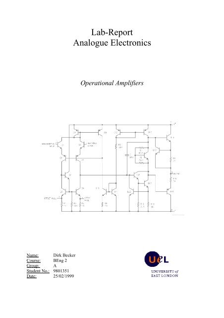
Lab-Report Analogue Electronics
Lab-Report Analogue Electronics
Lab-Report Analogue Electronics

You also want an ePaper? Increase the reach of your titles
YUMPU automatically turns print PDFs into web optimized ePapers that Google loves.
<strong>Lab</strong>-<strong>Report</strong><br />
<strong>Analogue</strong> <strong>Electronics</strong><br />
Operational Amplifiers<br />
Name: Dirk Becker<br />
Course: BEng 2<br />
Group: A<br />
Student No.: 9801351<br />
Date: 25/02/1999
1. Contents<br />
1. CONTENTS 2<br />
2. INTRODUCTION 3<br />
3. COMMON MODE GAIN 3<br />
a) Without nulling potentiometer 3<br />
b) Nulling potentiometer 4<br />
4. VOLTAGE AMPLIFICATION 5<br />
a) Bridge circuit 5<br />
b) Differential gain 6<br />
c) Common mode rejection ratio 7<br />
5. INSTRUMENTATION AMPLIFIER 8<br />
a) Common mode gain 8<br />
b) Differential gain 9<br />
c) Common mode rejection ratio (CMRR) 10<br />
d) Derivation of differential amplification 10<br />
Output differential amplifier 10<br />
ii. Input amplifier 11<br />
6. COMPARISON 741 VS. INSTRUMENTATION/STRAIN GAUGE AMPLIFIER 12<br />
7. CONCLUSUION 13<br />
2
¨<br />
¡<br />
2. Introduction<br />
Operational amplifiers were first used in the late 1940s for performing mathematical<br />
calculations, or so called operations like adding, subtracting, multiplication, etc.. Operational<br />
amplifiers are very common used since their availability on Integrated Circuits (ICs) in the<br />
1960s. For instance the LM341 was introduced in 1967.<br />
An operational amplifier is a very high gain differential amplifier with high input impedance<br />
and low output impedance. Today they are used in nearly all electronic circuits and replace<br />
numbers of discrete transistors.<br />
3. Common mode gain<br />
a) Without nulling potentiometer<br />
First part of the <strong>Lab</strong> was to determine the common mode gain at different input voltages. The<br />
common mode gain is the amplification of the opamp with no different input voltages. It<br />
should be usually 0, but practically a small voltage will occur at the output.<br />
<br />
¦¨¨ ©<br />
¦<br />
§ ¦<br />
<br />
¦¨ ©<br />
<br />
<br />
¦¨ ©<br />
¢ £ ¤ ¥ ¦<br />
<br />
<br />
<br />
¦¨¨ ©<br />
Measured values:<br />
V 1 =V 2 V Out A C<br />
0V -2.3mV 0<br />
5V 6.0mV 1.2*10 -3<br />
10V 14.3mV 1.43*10 -3<br />
where A C is defined as the common mode gain:<br />
VO<br />
A<br />
C<br />
=<br />
1<br />
(V1<br />
+ V2<br />
)<br />
2<br />
The higher the common input voltage, the higher the common mode gain (which is not<br />
wanted).<br />
3
) Nulling potentiometer<br />
For a better suppression of the common mode gain a nulling potentiometer can be connected<br />
to the most opamps. It is used to set the output voltage to 0V, when no differential input<br />
voltage is applied (common mode).<br />
<br />
<br />
<br />
!"<br />
The above figure shows the connection of a nulling potentiometer to a opam LM741, which<br />
was used in the <strong>Lab</strong>.<br />
The adjustable range of the nulling potentiometer with no different input voltage (V 1 =V 2 =0V)<br />
was: V max | V1=V2=0V =109.9mV (left end of potentiometer)<br />
V min | V1=V2=0V =-114.9mV (right end of potentiometer)<br />
When the potentiometer is adjusted so that V Out =0V at V 1 =V 2 =0V, the following output<br />
voltages and common mode gains can be obtained:<br />
V 1 =V 2 V Out A C<br />
5V 8.2mV 1.64*10 -3<br />
10V 16.5mV 1.65*10 -3<br />
The nulling potentiometer improves only the common mode gain for small input voltages. For<br />
higher input voltages the common mode gain is equal or greater than without nulling<br />
potentiometer. This results from the internal structure of the opamp LM341.<br />
4
4. Voltage Amplification<br />
a) Bridge circuit<br />
To generate two different voltages a bridge circuit should be connected together. The circuit<br />
diagram is shown below:<br />
. &/0<br />
&''( )* +,( )-<br />
)*<br />
&''(<br />
&''(<br />
# $ # %<br />
)*<br />
The bridge outputs were V 1 =7.5V and V 2 =7.67V.<br />
The calculated bridge voltages are:<br />
V<br />
V<br />
1Calc<br />
1Calc<br />
R<br />
=<br />
2R<br />
A<br />
A<br />
15V<br />
100kΩ<br />
= 15V = 7.5V<br />
200kΩ<br />
V<br />
V<br />
2Calc<br />
2Calc<br />
R<br />
A<br />
=<br />
R + R<br />
A<br />
B<br />
15V<br />
100kΩ<br />
= 15V = 7.81V<br />
192kΩ<br />
The difference between the calculated and the measured voltages result on the inaccurate<br />
values of the used resistors (+-5%). Although the measuring instruments have a small<br />
uncertainty.<br />
5
\]<br />
C D<br />
B A<br />
]<br />
b) Differential gain<br />
The outputs of the bridge should then be connected to the corresponding inputs of the<br />
operational amplifier from part 3) Common mode gain. The resulting circuit diagram is<br />
shown in the following figure:<br />
1 6<br />
8 9: 7<br />
7 6<br />
1 23 4 5<br />
The output voltages of the bridge change when the bridge is connected to the opamp stage<br />
because the amplifier inputs are a load to the bridge. The new bridge output voltages can be<br />
calculated using Thevenin’s theorem, where V 0 is the disconnected bridge voltage.<br />
; ?<br />
; @<br />
A<br />
C<br />
A<br />
C<br />
BJKLMNF<br />
FH EI<br />
EI<br />
FH<br />
FH EI<br />
FGH<br />
EF<br />
FGH<br />
EF<br />
FGGH ED<br />
FGGH ED<br />
; < =><br />
V<br />
R<br />
R<br />
01<br />
1<br />
= R<br />
A15V<br />
= 7.5V (for V<br />
1'<br />
)<br />
2<br />
1<br />
= R<br />
A<br />
= 50kΩ<br />
2<br />
= R + R = 110kΩ<br />
⇒ V<br />
1'<br />
=<br />
R<br />
V ' = 5.16V<br />
1<br />
01<br />
L<br />
1<br />
L<br />
2<br />
R<br />
L<br />
+ R<br />
01<br />
V<br />
01<br />
110kΩ<br />
= 7.5V<br />
160kΩ<br />
UVW<br />
The output voltages of the bridge decrease<br />
when connecting to the opamp-circuit<br />
because of it’s load function.<br />
\<br />
]<br />
X^<br />
bcdebfU<br />
XU<br />
U[[Z Xa<br />
UZ<br />
U[[Z<br />
XY<br />
`^Z X_<br />
O S<br />
XY<br />
U[Z \<br />
O T<br />
UZ<br />
U[Z XU<br />
XY<br />
UZ<br />
O P QR<br />
U[[Z X^<br />
U[[Z Xa<br />
U[[Z Xa<br />
6
The measured output values of the connected bridge were:<br />
V 1 ’=5.35V<br />
V 2 ’=5.32V at an output voltage V Out =513mV<br />
The difference between the calculated and the measured values of the bridge outputs (=the<br />
opamp input voltage) results from the inaccuracy values of the used resistors.<br />
Every resistor can have a tolerance of +-5% which can change the parameters of the circuit<br />
very much (worst case = all the devices have their maximum tolerance).<br />
From the above results the differential gain of the amplifier stage was to determine:<br />
A<br />
A<br />
A<br />
D<br />
D<br />
D<br />
VOut<br />
=<br />
V − V<br />
1<br />
0.513V<br />
=<br />
5.35V − 5.32V<br />
= 17.1<br />
2<br />
Calculated value of A D :<br />
A<br />
R<br />
=<br />
R<br />
100kΩ<br />
=<br />
10kΩ<br />
2<br />
D<br />
=<br />
1<br />
10<br />
c) Common mode rejection ratio<br />
A significant feature of a differential amplifier is that the signals which are opposite at the<br />
inputs are highly amplified, while those which are common to the two inputs are only slightly<br />
amplified. The ratio of the differential gain and the common mode gain is called the common<br />
mode rejection gain (CMRR).<br />
A<br />
CMRR =<br />
A<br />
CMRR<br />
dB<br />
D<br />
C<br />
≈<br />
17<br />
0.0015<br />
⎛ A<br />
= 20log<br />
⎜<br />
⎝ A<br />
D<br />
C<br />
= 8500<br />
⎞ ⎛<br />
⎟ ≈ 20log⎜<br />
⎠ ⎝<br />
17 ⎞<br />
⎟ = 79dB<br />
0.0015 ⎠<br />
7
o m p<br />
m n<br />
p o m<br />
g<br />
h<br />
5. Instrumentation Amplifier<br />
a) Common mode gain<br />
m o o p<br />
n q<br />
r m s<br />
n m<br />
r t i u<br />
r q s<br />
i j k l m<br />
n q<br />
v w x<br />
m o o p<br />
v w x<br />
After connection of the instrumentation amplifier circuit shown in the figure above the<br />
common mode gain was to determine and to compare with the differential amplifier from Part<br />
3) Common mode gain.<br />
A<br />
C<br />
=<br />
VO<br />
1<br />
(V1<br />
+ V2<br />
)<br />
2<br />
V 1 =V 2 V Out A C<br />
0V 0V 0<br />
5V 197mV 0.0394<br />
10V 197mV 0.0197<br />
The nulling potentiometer had to be aligned again, because the two additional connected<br />
amplifiers have each their own output voltage offset, which has to be compensated by the<br />
nulling potentiometer of the differential amplifier (the last opamp).<br />
The common mode gain is now larger than at the first part of the lab report, because the<br />
common mode gains of the 3 different opamps are resulting in a new common mode gain for<br />
the whole instrumentation amplifier.<br />
8
z<br />
{<br />
b) Differential gain<br />
The differential gain was again determined by connecting the bridge to the corresponding<br />
inputs of the amplifier.<br />
The circuit diagram of the connected bridge is shown below:<br />
| } } ~<br />
€<br />
‚ ƒ „ |<br />
€ ˆ<br />
| } ~<br />
|<br />
| } } ~<br />
€<br />
| } ~<br />
|<br />
The output voltages of the connected bridge are now nearly the same than the output voltages<br />
of the unconnected bridge, because they are only connected to the opamp inputs which have<br />
an input resistance of more than several hundreds kΩ( for the LM741 typically 2MΩ) .<br />
… † ‡<br />
V 1 =7.5V y<br />
(unconnected) V 1 =7.48V (connected)<br />
V 2 =7.67V y (unconnected) V 2 =7.7V (connected)<br />
V Out =6.44V<br />
hence the differential gain A C can be determined:<br />
A<br />
A<br />
D<br />
D<br />
VOut<br />
=<br />
V − V<br />
1<br />
= 29.3<br />
2<br />
6.44V<br />
=<br />
7.7V − 7.48V<br />
⎛ 2R<br />
C<br />
⎞ R<br />
2<br />
A<br />
C = ⎜1<br />
+<br />
R<br />
⎟<br />
C<br />
R1<br />
The theoretically calculated of A D is calculated by ⎝ ⎠<br />
100kΩ<br />
A C = 2 × = 30<br />
10kΩ<br />
So the measured value is very close to the theoretically calculated value. The deviation of<br />
both values results from the inaccuracy of the used resistors and of the not ideal opamp.<br />
9
“<br />
’<br />
‘<br />
Ž<br />
Ž<br />
‰‹Œ<br />
¥<br />
¦<br />
¦<br />
§ ¥<br />
c) Common mode rejection ratio (CMRR)<br />
The common mode rejection ratio is calculated using the equations from part c) Common<br />
mode rejection ratio.<br />
A<br />
CMRR =<br />
A<br />
CMRR<br />
dB<br />
D<br />
C<br />
≈<br />
29.3<br />
= 732.5<br />
0.04<br />
⎛ A<br />
= 20log<br />
⎜<br />
⎝ A<br />
D<br />
C<br />
⎞ ⎛ 29.3 ⎞<br />
⎟ ≈ 20log⎜<br />
⎟ = 57dB<br />
⎠ ⎝ 0.04 ⎠<br />
The CMRR is about ten times less than the CMRR of the single differential amplifier.<br />
d) Derivation of differential amplification<br />
i. Output differential amplifier<br />
‹‹<br />
‰‹Œ<br />
‹Œ ‰Š<br />
‘ ‹<br />
Superposition<br />
”••–<br />
—˜<br />
©£ ©£ª<br />
£¤ ¡¨<br />
£¤ ¡¢<br />
£¤ ¡¨<br />
©ªª<br />
—” š›œ”<br />
˜<br />
V<br />
V<br />
V<br />
V<br />
Out1<br />
V<br />
+<br />
V<br />
+<br />
R<br />
2<br />
=<br />
R + R<br />
Out1<br />
2<br />
'<br />
Out1<br />
R<br />
2<br />
+ R<br />
=<br />
R<br />
1<br />
R<br />
2<br />
+ R<br />
=<br />
R<br />
R<br />
=<br />
R<br />
2<br />
1<br />
1<br />
V<br />
2<br />
1<br />
2<br />
'<br />
1<br />
V<br />
1<br />
2<br />
'<br />
→ (V ' = 0V)<br />
R<br />
2<br />
R + R<br />
1<br />
1<br />
2<br />
R<br />
=<br />
R<br />
2<br />
1<br />
Vout<br />
V '<br />
V<br />
1<br />
2<br />
out 2<br />
R<br />
= −<br />
R<br />
R<br />
= −<br />
R<br />
2<br />
1<br />
2<br />
1<br />
V '<br />
1<br />
→<br />
(V ' = 0V)<br />
2<br />
”•–<br />
—”<br />
”•–<br />
—˜<br />
”••–<br />
žŸ<br />
10
´<br />
°<br />
¯<br />
¯<br />
°<br />
Now the two separate calculated voltages are added:<br />
V<br />
V<br />
V<br />
Out<br />
Out<br />
Out<br />
2<br />
= V<br />
R<br />
=<br />
R<br />
R<br />
=<br />
R<br />
1<br />
Out1<br />
2<br />
1<br />
2<br />
2<br />
VOut<br />
R<br />
=<br />
V ' −V ' R<br />
+ V<br />
2<br />
1<br />
2<br />
Out 2<br />
R<br />
V2<br />
' −<br />
R<br />
2<br />
1<br />
(V ' −V ')<br />
1<br />
= A<br />
D<br />
V<br />
1<br />
ii. Input amplifier<br />
(via Superposition and virtual earth)<br />
V 1 =0V<br />
¯<br />
°<br />
® «±<br />
® «¬<br />
² <br />
² ³ <br />
«±<br />
®<br />
V<br />
V<br />
V<br />
V<br />
21<br />
R<br />
C<br />
+ R<br />
D<br />
=<br />
2<br />
R<br />
D<br />
⎛ R ⎞<br />
C<br />
21 = ⎜1<br />
+<br />
R<br />
⎟<br />
D<br />
11<br />
⎝<br />
R<br />
= −<br />
R<br />
C<br />
D<br />
V<br />
2<br />
V<br />
⎠<br />
2<br />
V 2 =0V<br />
² ³<br />
² <br />
¯<br />
°<br />
® «±<br />
® «¬<br />
² ³<br />
V<br />
V<br />
21<br />
R<br />
C<br />
+ R<br />
D<br />
=<br />
1<br />
R<br />
D<br />
⎛ R<br />
C<br />
⎞<br />
12 = ⎜1<br />
+<br />
R<br />
⎟<br />
D<br />
V<br />
V<br />
22<br />
⎝<br />
R<br />
= −<br />
R<br />
C<br />
D<br />
V<br />
V<br />
⎠<br />
1<br />
1<br />
®<br />
² ³³<br />
«±<br />
11
Superposition of V 11 , V 12 and V 21 , V 22<br />
V ' = V<br />
V<br />
+ V<br />
R = −<br />
⎛ R + ⎜1<br />
+<br />
⎞<br />
V<br />
C<br />
C<br />
1 11 12<br />
2<br />
1<br />
R ⎜<br />
D<br />
R ⎟ ⎝ D ⎠<br />
⎛ R<br />
C<br />
⎞ R<br />
C<br />
2<br />
' = V21<br />
+ V22<br />
= ⎜1<br />
+ V2<br />
− V1<br />
R<br />
⎟<br />
D<br />
R<br />
D<br />
⎝<br />
V<br />
Now regarding to i) Input amplifier<br />
V ' − V ' = V<br />
2<br />
2<br />
1<br />
V ' − V ' =<br />
1<br />
2<br />
⎛ 2R<br />
⎜1<br />
+<br />
⎝ R<br />
D<br />
( −<br />
C<br />
V ) ⎜<br />
⎟ 2<br />
V1<br />
1<br />
⎝ R<br />
D ⎠<br />
C<br />
⎠<br />
⎞ ⎛ 2R<br />
⎟ − V<br />
⎜<br />
1<br />
1 +<br />
⎠ ⎝ R<br />
⎛ 2R +<br />
⎞<br />
D<br />
C<br />
⎟ ⎞<br />
⎠<br />
This equation now into<br />
VOut<br />
=<br />
V ' −V '<br />
2<br />
1<br />
R<br />
R<br />
2<br />
1<br />
= A<br />
D<br />
V<br />
V<br />
A<br />
Out<br />
Out<br />
D<br />
R<br />
2<br />
=<br />
2<br />
−<br />
R1<br />
R =<br />
2<br />
2<br />
R<br />
VOut<br />
=<br />
V − V<br />
2<br />
1<br />
( V ' V ')<br />
( V − V )<br />
1<br />
1<br />
1<br />
R =<br />
R<br />
2<br />
1<br />
⎛ 2R<br />
⎜1<br />
+<br />
⎝ R<br />
D<br />
C<br />
⎛ 2R<br />
⎜1<br />
+<br />
⎝ R<br />
D<br />
C<br />
⎞<br />
⎟<br />
⎠<br />
⎞<br />
⎟<br />
⎠<br />
or with the resistors from the <strong>Lab</strong><br />
A<br />
D<br />
=<br />
VOut<br />
V − V<br />
2<br />
1<br />
=<br />
R<br />
R<br />
2<br />
1<br />
⎛ 2R<br />
⎜1<br />
+<br />
⎝ R<br />
B<br />
A<br />
⎞<br />
⎟<br />
⎠<br />
QED<br />
6. Comparison 741 vs. instrumentation/strain gauge amplifier<br />
Item 741(C) RS strain gauge Amplifier<br />
V in +-15V +-12V<br />
I/P offset voltage 4mV 200µV<br />
I/P impedance >0.3 MΩ >5MΩ<br />
Bandwidth (unity gain) >437kHz 450kHz<br />
O/P voltage span +-12V V S -+2V<br />
O/P current +-25mA 5mA<br />
closed loop gain 30dB 3..60dB<br />
open loop gain -- >120dB<br />
CMRR 57dB >120dB<br />
Power dissipation 3x0.5W 0.5W<br />
max. bridge supply current -- 12mA<br />
Price 3x£0.50 £44.43<br />
12
7. Conclusuion<br />
Opamps are very unique electronic devices. Because of their in some cases nearly perfect<br />
characteristics it’s very easy to built up cheap and well working amplifiers.<br />
The opamp circuits have to be designed carefully and especially for instrumentation<br />
amplifiers the other used devices, like resistors must be selected very carefully in order to<br />
obtain correct results. For an instrumentation amplifier used for measuring it is very important<br />
to deliver exact results.<br />
13