Chapter 2. PIC 16F877 Microcontroller - MWFTR
Chapter 2. PIC 16F877 Microcontroller - MWFTR
Chapter 2. PIC 16F877 Microcontroller - MWFTR

You also want an ePaper? Increase the reach of your titles
YUMPU automatically turns print PDFs into web optimized ePapers that Google loves.
<strong>Chapter</strong> <strong>2.</strong> <strong>PIC</strong> <strong>16F877</strong> <strong>Microcontroller</strong> - Overview<br />
2<br />
<strong>Chapter</strong> <strong>2.</strong> <strong>PIC</strong> <strong>16F877</strong> <strong>Microcontroller</strong> - Overview<br />
1. <strong>PIC</strong> <strong>16F877</strong> Architecture<br />
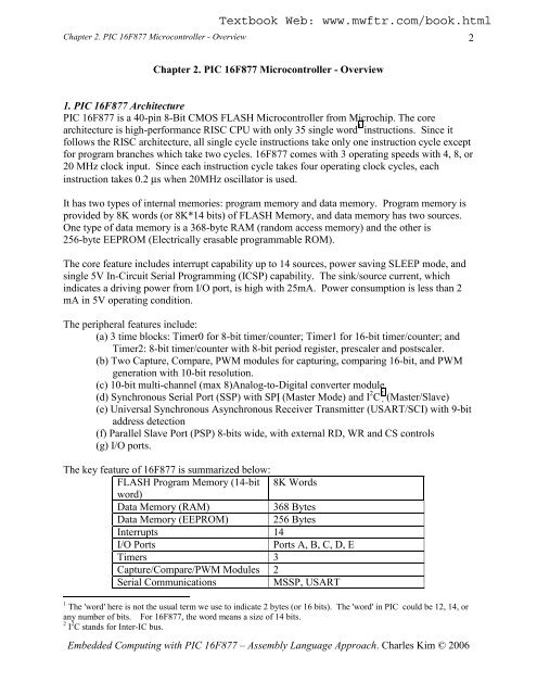
<strong>PIC</strong> <strong>16F877</strong> is a 40-pin 8-Bit CMOS FLASH <strong>Microcontroller</strong> from Microchip. The core<br />
architecture is high-performance RISC CPU with only 35 single word 1 instructions. Since it<br />
follows the RISC architecture, all single cycle instructions take only one instruction cycle except<br />
for program branches which take two cycles. <strong>16F877</strong> comes with 3 operating speeds with 4, 8, or<br />
20 MHz clock input. Since each instruction cycle takes four operating clock cycles, each<br />
instruction takes 0.2 µs when 20MHz oscillator is used.<br />
It has two types of internal memories: program memory and data memory. Program memory is<br />
provided by 8K words (or 8K*14 bits) of FLASH Memory, and data memory has two sources.<br />
One type of data memory is a 368-byte RAM (random access memory) and the other is<br />
256-byte EEPROM (Electrically erasable programmable ROM).<br />
The core feature includes interrupt capability up to 14 sources, power saving SLEEP mode, and<br />
single 5V In-Circuit Serial Programming (ICSP) capability. The sink/source current, which<br />
indicates a driving power from I/O port, is high with 25mA. Power consumption is less than 2<br />
mA in 5V operating condition.<br />
The peripheral features include:<br />
(a) 3 time blocks: Timer0 for 8-bit timer/counter; Timer1 for 16-bit timer/counter; and<br />
Timer2: 8-bit timer/counter with 8-bit period register, prescaler and postscaler.<br />
(b) Two Capture, Compare, PWM modules for capturing, comparing 16-bit, and PWM<br />
generation with 10-bit resolution.<br />
(c) 10-bit multi-channel (max 8)Analog-to-Digital converter module.<br />
(d) Synchronous Serial Port (SSP) with SPI (Master Mode) and I 2 C 2 (Master/Slave)<br />
(e) Universal Synchronous Asynchronous Receiver Transmitter (USART/SCI) with 9-bit<br />
address detection<br />
(f) Parallel Slave Port (PSP) 8-bits wide, with external RD, WR and CS controls<br />
(g) I/O ports.<br />
The key feature of <strong>16F877</strong> is summarized below:<br />
FLASH Program Memory (14-bit 8K Words<br />
word)<br />
Data Memory (RAM)<br />
368 Bytes<br />
Data Memory (EEPROM) 256 Bytes<br />
Interrupts 14<br />
I/O Ports<br />
Ports A, B, C, D, E<br />
Timers 3<br />
Capture/Compare/PWM Modules 2<br />
Serial Communications<br />
MSSP, USART<br />
1 The 'word' here is not the usual term we use to indicate 2 bytes (or 16 bits). The 'word' in <strong>PIC</strong> could be 12, 14, or<br />
any number of bits. For <strong>16F877</strong>, the word means a size of 14 bits.<br />
2 I 2 C stands for Inter-IC bus.<br />
Embedded Computing with <strong>PIC</strong> <strong>16F877</strong> – Assembly Language Approach. Charles Kim © 2006
<strong>Chapter</strong> <strong>2.</strong> <strong>PIC</strong> <strong>16F877</strong> <strong>Microcontroller</strong> - Overview<br />
3<br />
Parallel Communications<br />
10-bit Analog-to-Digital Module<br />
Instruction Set<br />
PSP<br />
8 channels<br />
35 Instructions<br />
<strong>2.</strong> Pin and Package<br />
There are three package types are available: DIP, PLCC, and QFP. This book assumes that we<br />
all use the DIP because of its best fit to breadboard or proto-board.<br />
1<br />
2<br />
3<br />
4<br />
5<br />
6<br />
7<br />
8<br />
9<br />
10<br />
11<br />
12<br />
13<br />
14<br />
15<br />
16<br />
17<br />
18<br />
19<br />
20<br />
MCLR/VPP/THV RB7/PGD<br />
RA0/AN0<br />
RB6/PGC<br />
RA1/AN1<br />
RB5<br />
RA2/AN2/VREF-<br />
RB4<br />
RA3/AN3/VREF+ RB3/PG<br />
RA4/TOCKI<br />
RA/AN4/SS<br />
RE0/RD/AN5<br />
RE1/WR/AN6<br />
RE2/CS/AN7<br />
V DD<br />
V SS<br />
<strong>PIC</strong><strong>16F877</strong>/874<br />
OSC1/CLKIN<br />
OSC2/CLKOUT<br />
RC0/T1OS0/T1CKI<br />
RC1/T1OS1/CCP2<br />
RC2/CCP1<br />
RC3/SCK/SCL<br />
RD0/PSP0<br />
RD1/PSP1<br />
RB2<br />
RB1<br />
RB0/INT<br />
V DD<br />
V SS<br />
RD7/PSP7<br />
RD6/PSP6<br />
RD5/PSP5<br />
RD4/PSP4<br />
RC7/RX/DT<br />
RC6/TX/CK<br />
RC5/SDO<br />
RC4/SDI/SDA<br />
RD3/PSP3<br />
RD2/PSP2<br />
40<br />
39<br />
38<br />
37<br />
36<br />
35<br />
34<br />
33<br />
32<br />
31<br />
30<br />
29<br />
28<br />
27<br />
26<br />
25<br />
24<br />
23<br />
22<br />
21<br />
Fig 1. <strong>PIC</strong> <strong>16F877</strong> IC Package: DIP<br />
Embedded Computing with <strong>PIC</strong> <strong>16F877</strong> – Assembly Language Approach. Charles Kim © 2006
<strong>Chapter</strong> <strong>2.</strong> <strong>PIC</strong> <strong>16F877</strong> <strong>Microcontroller</strong> - Overview<br />
4<br />
Table 1. Pin Description<br />
Pin Pin Name Description Pin Pin Name Description<br />
#<br />
#<br />
1 ~MCLR 21 RD2 PORTD.2<br />
2 RA0/AN0 PORTA.0 /Analog Channel 0 22 RD3 PORTD.3<br />
3 RA1/AN1 PORTA.1 /Analog Channel 1 23 RC4/SDI/SDA PORTC.4/SDI(for SPI)/SDA(for I 2 C)<br />
4 RA2/AN2 PORTA.2 /Analog Channel 2 24 RC5/SDO PORTC.5 /SDO (for SPI)<br />
5 RA3/AN3 PORTA.3 /Analog Channel 3 25 RC6/TX PORTC.6 /TX (for Serial Com.)<br />
6 RA4/T0CK1 PORTA.4 / External Clock for Timer 0 26 RC7/RX PORTC.7 /RX (for Serial Com.)<br />
7 RA5/AN4 PORTA.5 /Analog Channel 4 27 RD4 PORTD.4<br />
8 RE0/AN5 PORTE.0 /Analog Channel 5 28 RD5 PORTD.5<br />
9 RE1/AN6 PORTE.1 /Analog Channel 6 29 RD6 PORTD.6<br />
10 RE2/AN7 PORTE.2 /Analog Channel 7 30 RD7 PORTD.7<br />
11 Vdd +3 ~ +5V 31 Vss GND<br />
12 Vss GND 32 Vdd +3 V ~ +5 V<br />
13 OSC1/CLKIN Oscillator Connection /Clock In 33 RB0/INT PORTB.0/External Interrupt<br />
14 OSC2/CLKOUT Oscillator Connection / Clock Out 34 RB1 PORTB.1<br />
15 RC0/T1CK1 PORTC.0 /External Clock for Timer 1 35 RB2/PGM PORTB.2 /Programming Input<br />
16 RC1/CCP2 PORTC.1 /CCP2 36 RB3 PORTB.3<br />
17 RC2/CCP1 PORTC.2 /CCP1 37 RB4 PORTB.4<br />
18 RC3/SCK/SCL PORTC.3 /SCK(for SPI)/SCL(for I 2 C) 38 RB5 PORTB.5<br />
19 RD0 PORTD.0 39 RB6/PGC PORTB.6 /Debugger/ICSP<br />
20 RD1 PORTD.1 40 RB7/PGD PORTB.7 /Debugger/ICSP<br />
3. Block Diagram<br />
The internal schematic of <strong>PIC</strong><strong>16F877</strong> is illustrated in the following block diagram. In the block<br />
diagram, we first see built-in function modules in boxes such as PORTA, PORTB for inputs and<br />
outputs, a 10-bit Analog-to-Digital (AD) module, 3 timer modules (Timer 0, Timer 1, and Timer<br />
2), EEPROM, etc. We also see the modules are connected via internal data bus of 8-bit width.<br />
This is the reason why <strong>16F877</strong> is called an 8-bit microcontroller. Since the program memory<br />
(FLASH) is organized with 14-bit word, it's content is accessed (or fetched) via 14-bit program<br />
bus by the instruction register. Instruction registers are not in the file (RAM) area so is not<br />
accessible by program. Another internal register, program counter (PC) accesses the program<br />
memory location ("addressing") via 13 bit information. With 13 bits, the addressing range goes<br />
to 2 13 =2 3 *2 10 =8K word.<br />
RAM file registers for data are connected via 8-bit data bus. The W register is a user accessible<br />
register. As you see in the block diagram, W directly accesses the ALU and the 8-bit data bus.<br />
As we can see, there should be W involved to move data between modules and inside the file<br />
RAM, except via indirect addressing mode. This means that writing to the output ports is done<br />
via the W register. The details of the indirect addressing are discussed in the <strong>PIC</strong> instruction.<br />
Embedded Computing with <strong>PIC</strong> <strong>16F877</strong> – Assembly Language Approach. Charles Kim © 2006
<strong>Chapter</strong> <strong>2.</strong> <strong>PIC</strong> <strong>16F877</strong> <strong>Microcontroller</strong> - Overview<br />
5<br />
Fig. 2 <strong>PIC</strong><strong>16F877</strong> Block Diagram<br />
4. Program Memory<br />
The <strong>PIC</strong><strong>16F877</strong> has a 13-bit program counter (PC) capable of addressing an 8K word of<br />
program memory pace, and accessing a location above the physically implemented address will<br />
cause a wrap-around.<br />
The reset vector is at address 0000 and the interrupt vector is at address 0004 3 . Details of this<br />
will be discussed through out the book as related subjects pop up.<br />
3 All addresses are in hexadecimal number unless stated otherwise. Hexadecimal numbers are usually indicated by a<br />
multiple-digit number followed by a letter h. In assembly language programming, however, we indicate a<br />
hexadecimal number with preceding 0x followed by a multi-digit number. For example, 1001h and 0x1001 both<br />
indicate a 4 digit hexadecimal number 1001.<br />
Embedded Computing with <strong>PIC</strong> <strong>16F877</strong> – Assembly Language Approach. Charles Kim © 2006
<strong>Chapter</strong> <strong>2.</strong> <strong>PIC</strong> <strong>16F877</strong> <strong>Microcontroller</strong> - Overview<br />
6<br />
5. Data Memory (RAM)<br />
The data memory in RAM is partitioned into multiple banks (or pages) which contain the<br />
General Purpose Registers (GPR) and the Special Function Registers (SFR). The SFRs are<br />
already internally defined by the system so users are not allowed to override these registers.<br />
These are the main tools to utilize the built-in functions. In other words, assigning a port<br />
(PORTA, PORTB, etc) or a pin of a port as input or output, for example, is done using one or<br />
more of the SFRs. The GPRs are actually empty spaces to be used to store data or variables. In<br />
other words, when you define a variable like, x, y, or temp, then you have to allocate a space<br />
(a byte size) for each in the GPRs in RAM area. The registers in the RAM area are called file<br />
registers.<br />
Each bank extends to 7Fh (128 bytes). The lower locations of each bank are reserved for the<br />
SFRs. Above the SFRs are GPRs, implemented as static RAM. All implemented banks contain<br />
SFRs. Some “high use” SFRs, such as STATUS register, PCL register, FSR register, and<br />
INTCON register from one bank may be mirrored in another bank for code reduction and<br />
quicker access. For example, the STATUS register presents at 0003h (bank 0), 0083h(bank 1),<br />
0103h(bank 2), and 0183h(bank 3), simultaneously.<br />
To access registers properly, the bank location of them must be selected. In other words, you<br />
have keep track which bank of registers the CPU currently accesses. If the current bank access<br />
is Bank0, and your next register is located in Bank1, you have to select the Bank1 before<br />
accessing the register. The <strong>PIC</strong> CPU is very strict on the bank location. If we use an analogy of<br />
word processing, when we want to select a word, we have to move the cursor around the word<br />
then we click the mouse to select: without moving the cursor to the word, you do select the word<br />
you intend to do, it would select any word near the current cursor position. The selection of a<br />
bank is done by setting two bits of the STATUS register.<br />
Let's examine the file register map briefly. As mentioned above, the fourth register (address 03h,<br />
83h, 103h, and 183h) at each bank is assigned to STATUS register (see the Register file map).<br />
The STATUS register tells you about the status arithmetic and logical status. It also has very<br />
important function of selecting a bank.<br />
The detail of the STATUS register is shown below. Here, we highlight only bits of 6, 5, 2, and 0<br />
of the register. Note that the bit number of the byte of the register starts from 0 ending at 7. As<br />
we see, bits 5 and 6 of the register, as we indicate them as STATUS, are RP1 and RP0 bits<br />
which select banks. In other words, for example, if you access a register in bank 3, you have to<br />
set the two bits as 11, or STATUS=11b 4 . In this selection, we change each bit of a<br />
register. In such case, we may better use bit-oriented instruction (Details on instruction come<br />
later). STATUS is for Z flag to see if an operation results in zero or not.<br />
4 a letter following a number indicates that the number is a binary number. In assembly language programming, we<br />
use letter B followed by a single quote, a binary number, then a single quote to indicate a binary number. For<br />
example, B'01101100' represents in a code a binary number 01101100b.<br />
Embedded Computing with <strong>PIC</strong> <strong>16F877</strong> – Assembly Language Approach. Charles Kim © 2006
<strong>Chapter</strong> <strong>2.</strong> <strong>PIC</strong> <strong>16F877</strong> <strong>Microcontroller</strong> - Overview<br />
7<br />
Fig. 3 Register file map for SFRs and GPRs.<br />
Embedded Computing with <strong>PIC</strong> <strong>16F877</strong> – Assembly Language Approach. Charles Kim © 2006
<strong>Chapter</strong> <strong>2.</strong> <strong>PIC</strong> <strong>16F877</strong> <strong>Microcontroller</strong> - Overview<br />
8<br />
Fig 4. Details of the STATUS register<br />
Even though we have not formally discussed about instruction sets, it's always helpful to be<br />
exposed some instructions. So here is one example code to select bank for file register access.<br />
Every code in the book follows the Microchip MPLAB assembly programming notations and<br />
regulations (<strong>Chapter</strong> 3 explains about the MPLAB).<br />
This example is to send an output signal (the term 'output signal' means an either High (+5V) or<br />
Low (0 V)) to a pin of a port. A port has 8 pins and each pin can work either as an input or<br />
output. Each pin's assignment as input or output is determined by a bit assignment of a<br />
corresponding direction assignment file register.<br />
Fig 5. Port register and corresponding direction register<br />
Embedded Computing with <strong>PIC</strong> <strong>16F877</strong> – Assembly Language Approach. Charles Kim © 2006
<strong>Chapter</strong> <strong>2.</strong> <strong>PIC</strong> <strong>16F877</strong> <strong>Microcontroller</strong> - Overview<br />
9<br />
In practice, if you select a pin of PORTB as your output, then the corresponding direction<br />
assignment file register is TRISB register. TRISA is for PORTA, TRISC for PORTC, TRISD<br />
for PORTD, etc. If you want to use all 8 pins of PORTC as outputs, then you have to reset (or<br />
make 0) all 8 bits of TRISC. When you want to use the pin 1 of PORTC (notes as PORTC)<br />
as input and all others as outputs, then you set TRISC and reset all other bits of TRISC.<br />
Details of I/O port and settings come in next section. The example uses the pin0 of PORTB<br />
(noted as PORTB) as an output. We see that PROTB is in Bank 0 and its corresponding<br />
direction assignment TRISB is in Bank 1.<br />
;Example for Bank Selection<br />
;<br />
list P = <strong>16F877</strong><br />
;Target processor = <strong>16F877</strong><br />
;STATUS will select banks<br />
; 00 bank0<br />
; 01 bank1<br />
; 10 bank2<br />
; 11 bank3<br />
;<br />
;PORTB is in Bank 0<br />
;TRISB is in Bank 1<br />
;<br />
;Declaration of the SFRs –refer the file register map<br />
STATUS EQU 0x03 ;STATUS register is located in 03h (all 4 banks)<br />
PORTB EQU 0x06 ;PORTB in 06h (bank0)<br />
TRISB EQU 0x86 ;TRISB in 86h (bank1)<br />
; When started, bank 0 is automatically selected. So we are at bank 0 now<br />
; In other words STATUS=00<br />
; Now we want to access and write a byte information to TRISB<br />
; TRISB is in bank 1<br />
; Select bank1<br />
bsf STATUS, 0x05 ;set the 5 th bit of STATUS<br />
;now STATS=01<br />
movlw 0x00<br />
;load 00 to W register<br />
movwf TRISB<br />
;(W register is more like an accumulator)<br />
;store the value of W to TRISB register<br />
;Now all 8 pins of PORTB are used as outputs<br />
; Now let's access PORTB which is located in bank 0<br />
; bank 0 selection<br />
bcf STATUS, 0x05 ;now STATUS=00<br />
bsf PORTB, 0x00 ;meaning that set the bit 0 of PORTB<br />
;which means, send +5V output through the<br />
;pin 1 of PORTB.<br />
;If you connect an LED to PORTB, the LED<br />
;will turn on.<br />
; end of example<br />
end<br />
In the example code above, the prefix 0x indicate the number follows is a hexadecimal number.<br />
Also, a semicolon (;) starts a comment line of section. The program should end with end.<br />
6. Input/Output Ports<br />
Since we already have our example code involving PORTB and TRISB, one of the Input/Output<br />
(I/O) ports, it's the best time to explore the I/O ports of <strong>16F877</strong>. The I/O Ports are the simplest<br />
of peripherals and this is part of the reasons why the microcontroller was named by <strong>PIC</strong>, which<br />
stands for Peripheral Interface Controller. They allow the <strong>PIC</strong> to monitor and control external<br />
devices like sensors and relays. For most of the I/O Ports, the direction of I/O pins (input or<br />
Embedded Computing with <strong>PIC</strong> <strong>16F877</strong> – Assembly Language Approach. Charles Kim © 2006
<strong>Chapter</strong> <strong>2.</strong> <strong>PIC</strong> <strong>16F877</strong> <strong>Microcontroller</strong> - Overview<br />
10<br />
output) is controlled by the data direction register called TRIS register. A '1' for TRISB<br />
makes the pin PORTB an input, while a '0' makes an output. An easy way to remember of<br />
this input/output setting is that '1' looks like an alphabet I (Input) and '0' an O (Output). From the<br />
previous example code, since all 8 bits of TRISB are reset, all the pins of PORTB are selected as<br />
output:<br />
movlw 0x00<br />
movwf TRISB<br />
;TRISB=00000000<br />
;This makes all 8 pins of PORTB output pins<br />
When we want to make only PORTB as output and all other pins as input, we would do the<br />
following code revision.<br />
movlw 0xFD ;which is equivalent to (movlw b'11111101')<br />
movwf TRISB ;TRISB=11111101<br />
;PORTB as output, all other pins as input<br />
As you saw in the example code and above example, to send a value to any file register including<br />
the port registers like PORTB, PORTC, etc, you load a select number to W register, then move<br />
the content of W register to a file register.<br />
Figure below shows a typical I/O Port and read and writing operations. The writing to an I/O pin<br />
is to send data into a data latch. By the control of the TRIS, the data in available on the pin.<br />
Fig 6. Input (left) and Output (right) operation of a port register.<br />
Embedded Computing with <strong>PIC</strong> <strong>16F877</strong> – Assembly Language Approach. Charles Kim © 2006
<strong>Chapter</strong> <strong>2.</strong> <strong>PIC</strong> <strong>16F877</strong> <strong>Microcontroller</strong> - Overview<br />
11<br />
Then how do we actually write to the pin? In <strong>PIC</strong>, writing to a port is writing to a port register.<br />
This means you can send out all 8-bit information to a port, for example PORTB. Then, how do<br />
we write to a port? Writing to a port is to send data in W register to the port. In line with the<br />
first example code, let's write 11110000 to the pins of PORTB.<br />
bsf STATUS, 0x05 ;we are now in bank 1<br />
movlw 0x00<br />
;load 00 to W register<br />
movwf TRISB<br />
;PORTB pins are set as output<br />
bcf STATUS, 0x05 ;we are now in bank 0<br />
movlw 0xF0<br />
;W=11110000<br />
movwf PORTB<br />
;PORTB=11110000<br />
;B0=0, B1=0, B2=0, B3=0, B4=1,<br />
;B5=1, B6=1, B7=1<br />
When this code is running inside <strong>PIC</strong>, you can measure the voltage levels of the pins of PORTB<br />
to check the logical information's physical transformation at the pins. A measurement of B0<br />
would give you 0 volt and a measurement of B6 would indicate +5 volt (or the supply voltage to<br />
the Vdd pin of the <strong>PIC</strong> chip). So when you connect an LED to B6, you would see a lit LED.<br />
The above example code is to write a byte information. But we can send only 1 bit information<br />
too. This is done by using a bit-oriented instruction instead of a byte-oriented instruction. Let's<br />
turn on only B6 of the PORTB.<br />
bsf STATUS, 0x05 ;we are now in bank 1<br />
movlw 0x00<br />
;load 00 to W register<br />
movwf TRISB<br />
;PORTB pins are set as output<br />
bcf STATUS, 0x05 ;we are now in bank 0<br />
bsf PORTB, 0x06 ;Set the B6 of PORTB<br />
;All the pins are remained with the<br />
;previous values.<br />
Care should be exercised in port writing. The writing operation to a pin is, since writing is to<br />
write into a latch, actually so-called Read-Modify-Write. In other words, when you want send<br />
out '0' to a pin of a port by saying<br />
bcf<br />
PORTB, 0x00<br />
you may think that the CPU will just clear the bit so that the voltage at the pin is 0 volt. What<br />
actually happens is the whole port (PORTB register: 8 bits) is first read (READ), then the bit 0<br />
(single bit) is cleared (MODIFY), then finally new modified value (8 bits including the affected<br />
bit) is written (WRITE) back to the port of PORTB.<br />
Actually, any instruction that depends on a value currently in the register is going to be a Read-<br />
Modify-Write instruction. This includes ADDWF, SUBWF, BCF, BSF, INCF, XORWF, etc.<br />
Instructions that do not depend on the current register value, like MOVWF, CLRF, and so on are<br />
not R-M-W instructions.<br />
Let's consider an LED case. Suppose we make PORTB all outputs and drive the pins low. On<br />
each of the port pins is an LED connected to ground, such that a high output lights it. Let's<br />
Embedded Computing with <strong>PIC</strong> <strong>16F877</strong> – Assembly Language Approach. Charles Kim © 2006
<strong>Chapter</strong> <strong>2.</strong> <strong>PIC</strong> <strong>16F877</strong> <strong>Microcontroller</strong> - Overview<br />
12<br />
suppose that the processor is running very fast, say, at 20 MHz. Now if we go down the port<br />
setting each pin in order;<br />
bsf<br />
bsf<br />
bsf<br />
PORTB,0x00<br />
PORTB,0x01<br />
PORTB,0x02<br />
.<br />
.<br />
.<br />
we may see that only the last pin is set, and only the last LED actually turns on. Probably, all<br />
LEDs are dim, kind of half-on.<br />
Fig 7. Example of LEDs on PORTB<br />
This is because the LED takes a while to turn on. As each pin was set, the pin before it was not<br />
turned yet and so was read as a zero. This zero is written back out to the port latch (R-M-W)<br />
which clears the bit you just tried to set the instruction before. So we may have to have a few<br />
ms delays between the operations of LED.<br />
Another important consideration about the output at the pin is not the voltage level but the<br />
amount current can flow by the voltage. It is clear that there would not be any current when the<br />
pin voltage is 0 volt. However, it is not always clear how much current can a source with a +5<br />
volt provide to a connected load like LED. According to the specification of <strong>PIC</strong>, each pin can<br />
drive maximum 25 mA. In other words, if one device needs more than 25mA from the pin, your<br />
code may work but your pin cannot activate the device. Fortunately, however, most of devices<br />
like LED, relay, motor driver, motor control chip, and others do not require high current driving<br />
inputs. So we do not have to worry about the driving power of <strong>PIC</strong>, but we surely have to check<br />
when we connect any devise at the output pin of the <strong>PIC</strong> of this driving limit of 25mA.<br />
Let's further discuss about LED. Most LEDs have their characteristics specified at a current of 20<br />
mA. So now you see the maximum current driving ability of <strong>PIC</strong> is not just randomly<br />
determined. But we do not light an LED with full brightness; it would shorten the life time of<br />
the LED. So we usually add a resister in series to reduce the amount of current flowing through<br />
the LED. When current flows through an LED, there is a voltage drop across the LED. The<br />
voltage drop is not the same for all types of LEDs, but it is reasonably right to assume that the<br />
voltage drop is about 1.7 – <strong>2.</strong>0 volt. Therefore, when an LED with a series resistor is connected<br />
Embedded Computing with <strong>PIC</strong> <strong>16F877</strong> – Assembly Language Approach. Charles Kim © 2006
<strong>Chapter</strong> <strong>2.</strong> <strong>PIC</strong> <strong>16F877</strong> <strong>Microcontroller</strong> - Overview<br />
13<br />
to an output pin, then the resistor picks up about 3 volt. Now we all know that the resistor value<br />
will determine the current through the resistor and the LED. So if you want to have half the<br />
maximum brightness, you would want to have only 10 mA flowing. To make that, your resistor<br />
should be 3/0.01 = 300 ohm. In this selection, the resistor consumes about 30 mW therefore a<br />
resistor wattage rating of 1/8 W is more than enough.<br />
When we read data from a pin, we read it directly from the pin, without the latch involvement.<br />
Reading from input pins is the same as reading from the port to W register in assembly language<br />
programming.<br />
bsf STATUS, 0x05 ;we are now in bank 1<br />
movlw 0xFF<br />
;load FF to W register<br />
movwf TRISB<br />
;PORTB pins are set as input<br />
bcf STATUS, 0x05 ;we are now in bank 0<br />
movf PORTB,0 ;W now holds PORTB<br />
;the trailing 0 is for the destination<br />
;of the operation (chapter 3 discusses about<br />
;the direction of operation in detail.)<br />
;In short, 0 indicates the result is stored in W<br />
; 1 stores in a file register (but 1 is a<br />
; default value, so you do not see 1 in the<br />
; code.)<br />
The above byte-oriented file register reading can be replaced to a bit-oriented reading (and<br />
monitoring) if only one input pin is the interest.<br />
bsf STATUS, 0x05 ;we are now in bank 1<br />
movlw 0xFF<br />
;load FF to W register<br />
movwf TRISB<br />
;PORTB pins are set as input<br />
bcf STATUS, 0x05 ;we are now in bank 0<br />
btfss PORTB,0x06<br />
;test the B6 bit of file register PORTB<br />
;Skip the next line of instruction<br />
;if B6 is set.<br />
goto A ;if B6=1 this line is skipped.<br />
goto B ;<br />
It is enough for an example code with I/O description. And it's about time to discuss more on the<br />
instruction sets of <strong>PIC</strong>, and the coding and program development environment. <strong>Chapter</strong> 3 gives<br />
details about the instruction sets of <strong>PIC</strong> <strong>16F877</strong>.<br />
Embedded Computing with <strong>PIC</strong> <strong>16F877</strong> – Assembly Language Approach. Charles Kim © 2006