Micro- and Nanoscale Deformation Measurement of Surface and ...
Micro- and Nanoscale Deformation Measurement of Surface and ...
Micro- and Nanoscale Deformation Measurement of Surface and ...

Create successful ePaper yourself
Turn your PDF publications into a flip-book with our unique Google optimized e-Paper software.
56 Exp Mech (2007) 47: 51–62<br />
terned layer just below the embedded silica sphere in<br />
the plane z=jr, forz=0 at the sphere midplane.<br />
Experimental Procedure<br />
Specimen Imaging<br />
<strong>Micro</strong>scale surface patterned samples were imaged<br />
using an Olympus SZX-12 stereomicroscope <strong>and</strong> a<br />
640480 pixel Sony XC-77 monochrome CCD camera.<br />
The resolution <strong>of</strong> the imaged surface was 10 mm/pixel,<br />
producing a total field <strong>of</strong> view <strong>of</strong> 6.44.8 mm.<br />
Internally patterned samples were imaged using a<br />
zoom factor <strong>of</strong> 3.3, giving a resolution <strong>of</strong> 3 mm/pixel<br />
<strong>and</strong> a 1.91.4 mm field <strong>of</strong> view. Since both polymers<br />
used for microscale tests were completely transparent,<br />
a uniformly white background was positioned behind<br />
the specimens to provide contrast with the black paint<br />
speckles during testing. Nanoparticle coated specimens<br />
were imaged under a Leica DM-R fluorescent microscope<br />
(with Hg lamp excitation source) using a<br />
QImaging Retiga monochrome CCD camera with<br />
1,2801,024 pixel resolution. For surface coated specimens,<br />
a 50 long working distance objective lens with<br />
no camera relay lens was used, giving an image<br />
resolution <strong>of</strong> 134 nm/pixel <strong>and</strong> a total field <strong>of</strong> view <strong>of</strong><br />
roughly 170140 mm. Internally patterned samples<br />
were imaged slightly differently by adding a 0.63<br />
relay lens. This modified imaging set-up produced a<br />
resolution <strong>of</strong> 213 nm/pixel, with a total field <strong>of</strong> view<br />
roughly 270220 mm. <strong>Micro</strong>sphere embedded samples<br />
were imaged at a pixel resolution <strong>of</strong> 533 nm/pixel,<br />
which gives a pattern acceptable for correlation while<br />
allowing for a greater field <strong>of</strong> view. For all fluorescent<br />
nanoparticle patterns, the background was dark <strong>and</strong><br />
the spheres appeared white upon excitation when<br />
viewed with a black <strong>and</strong> white camera.<br />
Imaging conditions for the fluorescent nanoparticle<br />
coated specimens were adjusted to minimize any<br />
photobleaching <strong>of</strong> the fluorescent dye. If photobleaching<br />
induced variations in the emitted light intensity<br />
created significant changes in the imaged pattern, poor<br />
correlation <strong>and</strong> erroneous displacement measurements<br />
were observed. As expected, the intensity <strong>of</strong> the<br />
excitation light source significantly affected the rate<br />
<strong>of</strong> bleaching. For the surface patterned samples, the<br />
effect <strong>of</strong> excitation intensity on nanoparticle photobleaching<br />
was investigated by taking a series <strong>of</strong> timelapse<br />
images <strong>of</strong> undeformed patterned samples under<br />
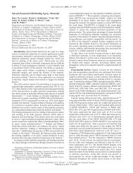
different lighting conditions. As shown in Fig. 5, light<br />
sources near the dye excitation frequency resulted in<br />
significant declines in the measured mean image<br />
Fig. 5 Mean intensity <strong>of</strong> nanoparticle patterned samples over<br />
time under excitation using a variety <strong>of</strong> illumination conditions<br />
intensity (labeled Bmax^ <strong>and</strong> Blow^). Greater stability<br />
in pixel intensity was obtained by lowering the<br />
intensity <strong>of</strong> the excitation light source <strong>and</strong> using<br />
auxiliary light sources at frequencies different from<br />
the peak excitation frequency <strong>of</strong> the fluorescent nanoparticles.<br />
For the internally embedded nanoparticle samples,<br />
a longer exposure time <strong>and</strong> less auxiliary light were<br />
necessary to produce images with the appropriate<br />
pattern contrast. These modifications did result in a<br />
slight increase in photobleaching rate compared to the<br />
surface patterned specimens. However, correlations<br />
performed on time-lapse images <strong>of</strong> undeformed specimens<br />
showed that photobleaching had no noticeable<br />
effect on the pattern quality or DIC measurements for<br />
the time scales associated with the testing in this work.<br />
Baseline Tests<br />
Noise levels associated with room vibrations, temperature<br />
fluctuations, etc., were determined by performing<br />
baseline tests in which no deformations was<br />
applied. Tests on both the surface <strong>and</strong> internally<br />
patterned microscale airbrushed samples showed an<br />
average r<strong>and</strong>om noise level <strong>of</strong> T0.5 mm (0.05 pixels).<br />
Conversely, baseline tests performed on the samples<br />
surface coated with nanoparticles displayed an average<br />
T7 nm (0.05 pixels) measured noise level in either<br />
direction, while the samples internally patterned with<br />
nanoparticles had an average <strong>of</strong> T18 nm (0.08 pixels)<br />
SEM