A Simple Electron Mobility Model Considering the Silicon ... - SBMicro
A Simple Electron Mobility Model Considering the Silicon ... - SBMicro
A Simple Electron Mobility Model Considering the Silicon ... - SBMicro

You also want an ePaper? Increase the reach of your titles
YUMPU automatically turns print PDFs into web optimized ePapers that Google loves.
A <strong>Simple</strong> <strong>Electron</strong> <strong>Mobility</strong> <strong>Model</strong> <strong>Considering</strong> <strong>the</strong><br />
<strong>Silicon</strong>-Dielectric Interface Orientation for Circular<br />
Surrounding-Gate Transistor<br />
André L. Perin 1,2 , Arianne S. N. Pereira 2 , Paula G. D. Agopian 1,3 , J.A. Martino 3 , and Renato Giacomini 1<br />
1 Centro Universitário da FEI, S. B. Campo, São Paulo, Brazil<br />
2 Universidade Metodista de São Paulo, S. B. Campo, São Paulo, Brazil,<br />
3 LSI/PSI/USP, University of São Paulo, Brazil,<br />
e-mail: andre.perin@metodista.br<br />
ABSTRACT<br />
AIn this work, a simple model that accounts for <strong>the</strong> variation of electron mobility as a function of <strong>the</strong> silicondielectric<br />
interface crystallographic orientation is presented. Simulations were conducted in order to compute<br />
<strong>the</strong> effective mobility of planar devices and its results were compared to experimental data for several interface<br />
orientations. The error between experimental data and <strong>the</strong> proposed model remained bellow 4%. The model<br />
has been applied to nMOS circular surrounding gate (thin-pillar transistor - CYNTHIA) and allowed <strong>the</strong> observation<br />
of current density variations as a function of <strong>the</strong> interface orientation around <strong>the</strong> silicon pillar.<br />
Index Terms: Circular, CYNTHIA, Microelectronics, <strong>Mobility</strong>, MuGFET.<br />
I. INTRODUCTION<br />
The use of <strong>Silicon</strong>-On-Insulator (SOI) technology<br />
allowed <strong>the</strong> development of smaller devices with better<br />
performance than <strong>the</strong> conventional silicon bulk transistors.<br />
Never<strong>the</strong>less, some undesired effects such as short<br />
channel effects are still present for smaller transistors.<br />
The use of multiple gate devices is pointed as one of <strong>the</strong><br />
possible solutions to minimize such short channel effects<br />
[1]. The Multiple-Gate Field Effect Transistors (Mu-<br />
GFETs) are devices with more than one gate, usually connected<br />
at <strong>the</strong> same potential, and can be built with threedimensional<br />
structures.<br />
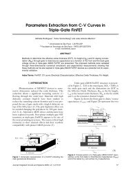
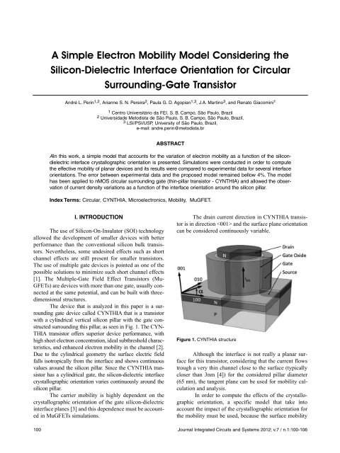
The device that is analyzed in this paper is a surrounding<br />
gate device called CYNTHIA that is a transistor<br />
with a cylindrical vertical silicon pillar with <strong>the</strong> gate constructed<br />
surrounding this pillar, as seen in Fig. 1. The CYN-<br />
THIA transistor offers superior device performance, with<br />
high sheet electron concentration, ideal subthreshold characteristics,<br />
and enhanced electron mobility in <strong>the</strong> channel [2].<br />
Due to <strong>the</strong> cylindrical geometry <strong>the</strong> surface electric field<br />
falls isotropically from <strong>the</strong> interface and shows continuous<br />
values around <strong>the</strong> silicon pillar. Since <strong>the</strong> CYNTHIA transistor<br />
has a cylindrical gate, <strong>the</strong> silicon-dielectric interface<br />
crystallographic orientation varies continuously around <strong>the</strong><br />
silicon pillar.<br />
The carrier mobility is highly dependent on <strong>the</strong><br />
crystallographic orientation of <strong>the</strong> gate silicon-dielectric<br />
interface planes [3] and this dependence must be accounted<br />
in MuGFETs simulations.<br />
The drain current direction in CYNTHIA transistor<br />
is in direction and <strong>the</strong> surface plane orientation<br />
can be considered continuously variable.<br />
Figure 1. CYNTHIA structure<br />
Although <strong>the</strong> interface is not really a planar surface<br />
for this transistor, considering that <strong>the</strong> current flows<br />
trough a very thin channel close to <strong>the</strong> surface (typically<br />
closer than 3nm [4]) for <strong>the</strong> considered pillar diameter<br />
(65 nm), <strong>the</strong> tangent plane can be used for mobility calculation<br />
and analysis.<br />
In order to compute <strong>the</strong> effects of <strong>the</strong> crystallographic<br />
orientation, a specific model that take into<br />
account <strong>the</strong> impact of <strong>the</strong> crystallographic orientation for<br />
<strong>the</strong> mobility must be used, because <strong>the</strong> surface mobility<br />
100 Journal Integrated Circuits and Systems 2012; v.7 / n.1:100-106
A <strong>Simple</strong> <strong>Electron</strong> <strong>Mobility</strong> <strong>Model</strong> <strong>Considering</strong> <strong>the</strong> <strong>Silicon</strong>-Dielectric Interface Orientation for Circular Surrounding-Gate Transistor<br />
Perin, Pereira, Agopian, Martino, & Giacomini<br />
may be reduced down to 60% depending on <strong>the</strong> current<br />
and interface crystallographic orientations [5]. Some<br />
commercial device simulators are able to account for <strong>the</strong><br />
current direction influence on mobility, but none of <strong>the</strong>m<br />
considers <strong>the</strong> silicon-dielectric interface plane orientation<br />
until now, what has lead some researchers to develop ad<br />
hoc solutions, like dividing <strong>the</strong> transistors in several<br />
regions and attributing different initial mobility parameters<br />
to each region. Goebel et al.[5], for instance, modeled<br />
a 900nm diameter CYNTHIA device in [5] by dividing<br />
<strong>the</strong> vertical sidewall of <strong>the</strong> cylinder in 72-fold polyhedron,<br />
thus <strong>the</strong> device consisted of 72 discrete parallel<br />
MOSFETs with current flowing in <strong>the</strong> (100) direction.<br />
Therefore, <strong>the</strong> single element’s crystallographic orientation<br />
was changed by steps of 5 degrees. The total current<br />
was obtained by <strong>the</strong> sum of <strong>the</strong> terminal currents of each<br />
single MOSFET element using 2-D simulations. The<br />
authors obtained results very close to experimental but<br />
this ad hoc solution is not applicable to smaller devices<br />
because <strong>the</strong> interaction between <strong>the</strong> transistor slices<br />
should be considered.<br />
The present work proposes a very simple local<br />
mobility model that was implemented in a 3D numerical<br />
simulator, by using <strong>the</strong> provided C interpreter, for <strong>the</strong><br />
simulation of <strong>the</strong> circular surrounding gate transistor<br />
CYNTHIA. The implemented model was also combined<br />
with doping concentration and temperature dependencies,<br />
based on <strong>the</strong> work of Caughey and Thomas [6] and<br />
Selberherr modeling [7,8] for mobility. The analysis of<br />
<strong>the</strong> proposed model was made from three-dimensional<br />
simulations of a CYNTHIA device.<br />
II. PROPOSED SURFACE-DEPENDENT<br />
ELECTRON MOBILITY MODEL<br />
The numerical device simulators offer a large set<br />
of mobility models and options because <strong>the</strong> mobility<br />
depends on different variables as device geometry, materials,<br />
bias, and temperature. There is no closed and universal<br />
model to carrier’s mobility. Thus, some physical<br />
issues on mobility degradation nature must be addressed<br />
before <strong>the</strong> proposition of an analytical formula.<br />
In order to facilitate <strong>the</strong> parameter extraction and<br />
simulator implementation <strong>the</strong> several physical degradation<br />
mechanisms are usually modeled separately and <strong>the</strong>n<br />
combined using a Matthiessen-like rule. This unrefined<br />
approximation if used under <strong>the</strong> correct conditions and<br />
limitations, can lead to very good results [9].<br />
The proposed model considers <strong>the</strong> mobility variation<br />
based on crystallographic orientation and <strong>the</strong> distance<br />
from <strong>the</strong> interface in addition to <strong>the</strong> o<strong>the</strong>r dependencies<br />
such as temperature, doping level, partial ionization<br />
of impurities, and transversal field dependencies.<br />
The degradation mechanisms that appear as a<br />
result of <strong>the</strong> substantially higher surface scattering near<br />
<strong>the</strong> interface between semiconductor and insulator [8]<br />
Journal Integrated Circuits and Systems 2012; v.7 / n.1:100-106<br />
occur inside inversion layers and can be associated to <strong>the</strong><br />
mobility degradation due to interface crystallographic<br />
orientation. The surface scattering is highly dependent on<br />
<strong>the</strong> physical interface proximity, due to influence of surface<br />
roughness. The carrier-carrier scattering, also affects<br />
<strong>the</strong> inversion layer [1] due to high carrier density that<br />
happens in this region. These effects must all be accounted<br />
for in order to perform accurate simulations. The<br />
transverse electric field is <strong>the</strong> main parameter that indicates<br />
<strong>the</strong> strength of inversion layer phenomena and<br />
varies according to <strong>the</strong> distance from <strong>the</strong> silicon-dielectric<br />
interface.<br />
The interface roughness depends on <strong>the</strong> manufacturing<br />
process, that is related to <strong>the</strong> oxide formation<br />
process, to <strong>the</strong> materials, to <strong>the</strong> silicon etch and also to <strong>the</strong><br />
crystalline surface orientation. Depending on <strong>the</strong> surface<br />
orientation, <strong>the</strong> amount of silicon atoms that are exposed to<br />
interaction with oxygen and o<strong>the</strong>r interface elements may<br />
vary, what changes <strong>the</strong> uniformity of <strong>the</strong> chemical links,<br />
affecting <strong>the</strong> interface quality and <strong>the</strong> dielectric thickness.<br />
Some authors attribute and model <strong>the</strong> interface roughness<br />
just to <strong>the</strong> fluctuation of <strong>the</strong> oxide thickness from its average<br />
value [10]. However, <strong>the</strong>re is a strong dependence of<br />
<strong>the</strong> carrier’s mobility on <strong>the</strong> roughness, and consequently<br />
on <strong>the</strong> surface orientation. Table 1 presents some data from<br />
two references that show good agreement to each o<strong>the</strong>r.<br />
The differences between <strong>the</strong>m are expected because <strong>the</strong><br />
data was extracted from different device types.<br />
Table 1. Relative electron experimental effective mobility for different<br />
surface orientations.<br />
Authors (ref) Reference Intermediate (110)<br />
(100)<br />
James E. Chung et al [11] 100% 93% (8 deg<br />
from )<br />
B. Goebel at al [5] 100% 97% (10 deg 60%<br />
from )<br />
The surrounding-gate transistor CYNTHIA has a<br />
circular cross section that implies in continuous variation<br />
of crystal orientation at <strong>the</strong> silicon dielectric interface,<br />
where <strong>the</strong> tangent planes at <strong>the</strong> interface can be considered<br />
to define a specific orientation, as seen on Fig. 2. On<br />
<strong>the</strong> o<strong>the</strong>r hand, ordinary multiple-gate devices have different<br />
crystallographic orientations to be considered related<br />
to defined <strong>the</strong> interface planes.<br />
In order to define a simple and consistent mobility<br />
model, a two-steps strategy was adopted. The first step was<br />
defining a function that accounts for <strong>the</strong> mobility inside <strong>the</strong><br />
inversion layer and depends on <strong>the</strong> azimuth angle . This<br />
function should be able to reproduce <strong>the</strong> surface mobility<br />
variation based on <strong>the</strong> crystallographic orientation over <strong>the</strong><br />
whole transistor body. The second step was choosing a<br />
function that could account for <strong>the</strong> mobility degradation as<br />
a function of <strong>the</strong> interface distance, which means that <strong>the</strong><br />
mobility should vary softly from <strong>the</strong> smaller value at <strong>the</strong><br />
interface to <strong>the</strong> greater value at <strong>the</strong> device body.<br />
101
A <strong>Simple</strong> <strong>Electron</strong> <strong>Mobility</strong> <strong>Model</strong> <strong>Considering</strong> <strong>the</strong> <strong>Silicon</strong>-Dielectric Interface Orientation for Circular Surrounding-Gate Transistor<br />
Perin, Pereira, Agopian, Martino, & Giacomini<br />
The first function, that defines a surface mobility<br />
µ S (α), must have some properties as consequence of <strong>the</strong><br />
crystal symmetry properties and <strong>the</strong> physical mobility<br />
issues. The first property is that <strong>the</strong> maximum value of<br />
µ S (α) must be acquired at α = 0, corresponding to <strong>the</strong><br />
direction or interface plane (100), and <strong>the</strong> minimum<br />
value of µ S (α) must be obtained at α = π/4, direction<br />
or interface plane (110).<br />
The second property to be considered is related to<br />
<strong>the</strong> periodicity of <strong>the</strong> crystal structure, <strong>the</strong> crystal structure<br />
has period of π/2, what means that <strong>the</strong> same values<br />
of <strong>the</strong> mobility will be found at each π/2 radians added to<br />
a reference angle π.<br />
The coefficients used in equation (2) are used as<br />
fitting parameters, and <strong>the</strong>se values will be obtained from<br />
<strong>the</strong> mobility values depending on <strong>the</strong> orientation. The<br />
number of coefficients that gives an accurate result is a<br />
function of how much <strong>the</strong> reference mobility function is<br />
different from <strong>the</strong> fundamental sinusoid. In this work,<br />
were defined, for comparison, two different equations, as<br />
seen on Fig. 3, <strong>the</strong> first, equation (2a), with <strong>the</strong> first and<br />
second term of equation (2), and <strong>the</strong> second, equation<br />
(2b), with <strong>the</strong> first, <strong>the</strong> second, <strong>the</strong> third, and fourth term<br />
of equation (2). Equations (2a) and (2b) were used in<br />
comparison with experimental results and both equations<br />
have good fit to experimental results and <strong>the</strong> choice of<br />
ei<strong>the</strong>r equation to use in three-dimensional simulations is<br />
a matter of commitment to simplicity and performance<br />
against <strong>the</strong> precision of <strong>the</strong> calculation.<br />
(2a)<br />
(2b)<br />
Figure 2. Cross Section of <strong>the</strong> CYNTHIA Device<br />
The third property defines that <strong>the</strong> mobility is<br />
always greater than zero in any value of <strong>the</strong> angle α, since<br />
physically <strong>the</strong>re is no negative value of mobility.<br />
The fourth and last property is related to <strong>the</strong> curve<br />
definition and defines that <strong>the</strong> chosen function should be<br />
an even function for any value of <strong>the</strong> angle α and also for<br />
α+π/4. This definition implies that <strong>the</strong> surface mobility<br />
µ S (α) = µ S (-α) and µ S (α+π/4) = µ S (-α+π/4), considering<br />
α as a real number.<br />
A Fourier series was considered as a base equation,<br />
as seen on equation (1), and removing all <strong>the</strong> unnecessary<br />
terms as defined by <strong>the</strong> four properties described<br />
above.<br />
(1)<br />
Since <strong>the</strong> surface mobility function is an even<br />
function, all <strong>the</strong> b n coefficients are assumed to be equal<br />
zero, because of fourth property and all <strong>the</strong> coefficients<br />
not multiple of four are equal zero, because of <strong>the</strong> second<br />
property. Then, <strong>the</strong> angle-dependent surface mobility<br />
function can be calculated from equation (2).<br />
(2)<br />
Figure 3. Surface mobility as a function of interface angle<br />
The second function defines <strong>the</strong> mobility variation<br />
as a function of distance from <strong>the</strong> interface and must be<br />
parameterized to fit <strong>the</strong> mobility value at <strong>the</strong> surface<br />
µ S (α), <strong>the</strong> mobility value at <strong>the</strong> center of device, now<br />
defined as µ b or body mobility, and <strong>the</strong> transition from<br />
one to o<strong>the</strong>r. The transition curve must have soft slope for<br />
µ S (α) in function of <strong>the</strong> interface distance. The equation<br />
(3) was chosen [8]:<br />
(3)<br />
Where, y is <strong>the</strong> distance from <strong>the</strong> silicon-oxide<br />
interface at <strong>the</strong> calculated point, and y ref is <strong>the</strong> reference<br />
distance from <strong>the</strong> oxide interface, that is used to set <strong>the</strong><br />
slope curve. The resulting curve obtained from <strong>the</strong> equation<br />
(3) is shown on Fig. 4.<br />
102 Journal Integrated Circuits and Systems 2012; v.7 / n.1:100-106
A <strong>Simple</strong> <strong>Electron</strong> <strong>Mobility</strong> <strong>Model</strong> <strong>Considering</strong> <strong>the</strong> <strong>Silicon</strong>-Dielectric Interface Orientation for Circular Surrounding-Gate Transistor<br />
Perin, Pereira, Agopian, Martino, & Giacomini<br />
Equation (4) presents <strong>the</strong> position dependent<br />
mobility, which also takes into account <strong>the</strong> influence of<br />
electric field, as proposed in [8]. It is composed by <strong>the</strong><br />
two defined functions (Eq. 3 and 2a or 2b), and <strong>the</strong> additional<br />
dependence on <strong>the</strong> transversal electric field given<br />
by Eq. (3).<br />
(4)<br />
Where µ S is <strong>the</strong> surface mobility as defined by<br />
equations (2a) or (2b), µ b is <strong>the</strong> body mobility as defined<br />
in [8], F(y) is <strong>the</strong> proximity function defined by equation<br />
(3), E is <strong>the</strong> electric field at <strong>the</strong> calculated point, E ref is <strong>the</strong><br />
reference electric field, used as an adjusting parameter,<br />
and β is <strong>the</strong> temperature dependent coefficient.<br />
Simulations were conducted and compared with<br />
well-known and published results for planar bulk devices<br />
in order to verify and set parameters and behavior of <strong>the</strong><br />
proposed model. The chosen device was a conventional<br />
nMOSFETs with channel length of 500 nm, gate oxide<br />
thickness of 9 nm, source and drain length of 250 nm and<br />
junction depth of 80 nm. The substrate doping concentration<br />
(p-type) was 1x10 17 cm -3 and source and drain doping<br />
concentration (n-type) was 1x10 20 cm -3 . This specific<br />
device was used to compare <strong>the</strong> results generated by <strong>the</strong><br />
surface mobility model with <strong>the</strong> previous published experimental<br />
results. This particular device is similar to <strong>the</strong> one<br />
measured by Goebel et all [5], adopted here as a reference.<br />
The simulations were computed using α angle measured<br />
from (100) plane orientation, and ranging from 0 to π/4<br />
rad, with device biased in triode with 100mV between<br />
source and drain and gate voltage varying from 0 to 1.2V.<br />
Fig. 6 shows <strong>the</strong> maximum transconductances<br />
extracted by <strong>the</strong> first derivative method. The resulting<br />
curve presents <strong>the</strong> same trend of <strong>the</strong> surface mobility.<br />
Fig. 7 shows <strong>the</strong> effective mobility normalized by<br />
<strong>the</strong> mobility value of <strong>the</strong> α = 0 direction. Results obtained<br />
from proposed model were compared with <strong>the</strong> experimental<br />
and <strong>the</strong> results show that <strong>the</strong> Four Term Proposed<br />
Figure 4. Interface distance transition slope<br />
The value of µ POS is maximum at <strong>the</strong> center of<br />
device because <strong>the</strong>re is no influence of <strong>the</strong> interface (F(y)<br />
= 1) and minimal at <strong>the</strong> interface where <strong>the</strong>re is degradation<br />
caused by interface and <strong>the</strong> electric field is higher.<br />
III. FITTING PARAMETERS<br />
Experimental results that show a 40% decrease in<br />
<strong>the</strong> surface mobility depending on <strong>the</strong> current and interface<br />
crystallographic orientation [5] were used to adjust<br />
<strong>the</strong> µ S (α) coefficients. After adjustment of <strong>the</strong> surface<br />
mobility, µ S (α), <strong>the</strong> complete equation of µ POS was<br />
implemented considering <strong>the</strong> standard values presented<br />
in [6], [7] and [8]. The complete function of µ POS was<br />
computed and plotted for different interface distances<br />
from <strong>the</strong> interface, as seen on Fig. 5, where <strong>the</strong> values of<br />
<strong>the</strong> applied coefficients a 0 , 4a 4 , 8a 8 and 12a 12 are 0.7825,<br />
0.2264, 0.02236 and -0.0309 (all in cm 2 /Vs) respectively.<br />
<strong>Considering</strong> <strong>the</strong> two effects, <strong>the</strong> resulting mobility has its<br />
lower value at <strong>the</strong> gate oxide interface and for <strong>the</strong> alpha<br />
angle value of π/4 rad; and <strong>the</strong> maximum mobility value<br />
is obtained at <strong>the</strong> device center where <strong>the</strong> interface crystallographic<br />
orientation doesn’t have an effect on <strong>the</strong><br />
resulting mobility independently of <strong>the</strong> considered angle.<br />
Journal Integrated Circuits and Systems 2012; v.7 / n.1:100-106<br />
Figure 5. Position Dependent <strong>Mobility</strong> Functions plotted with Two<br />
and Four Term Proposed <strong>Model</strong>s for different interface distances.<br />
Figure 6. Maximum transconductances in function of α obtained<br />
using <strong>the</strong> Four Term Proposed <strong>Model</strong> from α = 0 to 4 º.<br />
103
A <strong>Simple</strong> <strong>Electron</strong> <strong>Mobility</strong> <strong>Model</strong> <strong>Considering</strong> <strong>the</strong> <strong>Silicon</strong>-Dielectric Interface Orientation for Circular Surrounding-Gate Transistor<br />
Perin, Pereira, Agopian, Martino, & Giacomini<br />
Figure 7. Normalized Effective <strong>Mobility</strong> of Proposed <strong>Model</strong>s compared<br />
with Experimental Results [5]<br />
<strong>Model</strong> gives an excellent fit to experimental data and <strong>the</strong><br />
Two Term Proposed <strong>Model</strong> has <strong>the</strong> same trends but <strong>the</strong><br />
results are less accurate.<br />
The mobility profiles given by <strong>the</strong> proposed<br />
model implemented in Atlas device simulator of <strong>the</strong><br />
CYNTHIA transistor are plotted in Fig. 10 considering<br />
<strong>the</strong> cut lines starting at <strong>the</strong> center of <strong>the</strong> device and stopping<br />
at <strong>the</strong> silicon-dielectric for several values of α angle,<br />
considering α=0º at <strong>the</strong> plane (100) and α=45º at <strong>the</strong><br />
plane (110). The plot shows clearly <strong>the</strong> variation of<br />
mobility at <strong>the</strong> edges of <strong>the</strong> device and <strong>the</strong> maximum<br />
mobility value achieved in <strong>the</strong> center of <strong>the</strong> device. The<br />
difference between <strong>the</strong> curves remarks <strong>the</strong> different<br />
mobility profiles according to <strong>the</strong> variation of crystallographic<br />
orientation.<br />
The electron current density shows different distribution<br />
and <strong>the</strong> values are greater at 0º, 90º, 180º and<br />
270º due to <strong>the</strong> greater mobility at <strong>the</strong>se locations. Fig. 11<br />
presents <strong>the</strong> profiles of electron current density as a function<br />
of <strong>the</strong> α angle obtained at V GS = 1,2V.<br />
It’s also observed that <strong>the</strong> center of <strong>the</strong> body<br />
remains with <strong>the</strong> lowest current density, due to <strong>the</strong> lower<br />
carrier availability. The variation of <strong>the</strong> electron current<br />
density has <strong>the</strong> same tendency that <strong>the</strong> variation of mobility,<br />
as function of <strong>the</strong> angle α.<br />
The observed large current density variation may<br />
lead to a wide variation range of local degradation and to<br />
higher local temperatures, which may reduce <strong>the</strong> device<br />
reliability. Some previously considered symmetry advana)<br />
IV. CYNTHIA SIMULATION<br />
CYNTHIA transistors were simulated using two different<br />
mobility models, <strong>the</strong> proposed model (surface mobility<br />
degradation model) and <strong>the</strong> low field mobility model<br />
proposed by Caughey and Thomas [6] (Analytic). The simulated<br />
devices were nMOS transistors with channel length<br />
of 130, 150 and 180nm, diameter of 20, 30, 45, 55 and<br />
65nm, gate oxide thickness of 2.5nm, source and drain<br />
length of 65nm. The doping concentrations were 1x10 20 cm -<br />
3 at source and drain and 1x10 15 cm -3 at <strong>the</strong> channel. The<br />
studied devices were biased in triode with 50mV between<br />
source and drain and <strong>the</strong> gate voltage ranged from 0 to 1.2V.<br />
The simulation results of <strong>the</strong> proposed model<br />
showed lower values of drain current in comparison with<br />
<strong>the</strong> results obtained with <strong>the</strong> standard model, even though<br />
both have started with <strong>the</strong> same initial mobility, as shown<br />
on Fig. 8, due to <strong>the</strong> degradation of mobility depending<br />
on <strong>the</strong> interface proximity and <strong>the</strong> mobility variation as a<br />
function of <strong>the</strong> crystallographic orientation.<br />
The observation of important internal variables of<br />
<strong>the</strong> device, such as current density at <strong>the</strong> surface of device,<br />
was possible due to <strong>the</strong> implementation of <strong>the</strong> proposed<br />
model using <strong>the</strong> C Interpreter of ATLAS Simulator, such<br />
observation was not possible with o<strong>the</strong>r models, because<br />
<strong>the</strong> mobility computation did not take into account <strong>the</strong> crystallographic<br />
orientation, what leaded to a unreal distribution<br />
of mobility values at <strong>the</strong> whole device body.<br />
Ano<strong>the</strong>r internal variable that was studied was <strong>the</strong><br />
electric field, seen on Fig. 9. The lower values occur at <strong>the</strong><br />
center of device and, <strong>the</strong> higher values occur at <strong>the</strong> silicondielectric<br />
interface, because <strong>the</strong> electric field is radially uniform<br />
and, decreases as <strong>the</strong> distance from interface gets high.<br />
The potential distribution is also radially constant,<br />
like <strong>the</strong> electric field and <strong>the</strong>re is no variation of <strong>the</strong> values<br />
as function of <strong>the</strong> angular position.<br />
b)<br />
Figure 8. Drain Current results for a) Proposed <strong>Model</strong> and b)<br />
Standard <strong>Model</strong>.<br />
104 Journal Integrated Circuits and Systems 2012; v.7 / n.1:100-106
A <strong>Simple</strong> <strong>Electron</strong> <strong>Mobility</strong> <strong>Model</strong> <strong>Considering</strong> <strong>the</strong> <strong>Silicon</strong>-Dielectric Interface Orientation for Circular Surrounding-Gate Transistor<br />
Perin, Pereira, Agopian, Martino, & Giacomini<br />
Figure 9. Distribution of electric field, in log scale, in <strong>the</strong> cross<br />
section of CYNTHIA device<br />
Figure 10. <strong>Mobility</strong> profiles of a cross section of <strong>the</strong> simulated<br />
CYNTHIA device as function of <strong>the</strong> α angle.<br />
Figure 11. <strong>Electron</strong> current density profiles in <strong>the</strong> cross section of<br />
CYNTHIA device as function of <strong>the</strong> α angle.<br />
Figure 12. Distribution of current density in <strong>the</strong> cross section of<br />
CYNTHIA device biased with a) 0.25V, b) 0.45V and c) 1.2V at<br />
<strong>the</strong> gate.<br />
Journal Integrated Circuits and Systems 2012; v.7 / n.1:100-106<br />
105
A <strong>Simple</strong> <strong>Electron</strong> <strong>Mobility</strong> <strong>Model</strong> <strong>Considering</strong> <strong>the</strong> <strong>Silicon</strong>-Dielectric Interface Orientation for Circular Surrounding-Gate Transistor<br />
Perin, Pereira, Agopian, Martino, & Giacomini<br />
tages of CYNTHIA devices over squared cross-section<br />
devices [2] must be readdressed after <strong>the</strong> new possibility<br />
of observing <strong>the</strong> interface orientation influences, trough<br />
<strong>the</strong> proposed model.<br />
The current density analysis that follows shows<br />
different behaviors for different gate bias. The transistor<br />
with <strong>the</strong> gate biased in subthreshold region (V GS = 0.25V,<br />
V TH = 0.45V) presents four channels with higher current<br />
density aligned to <strong>the</strong> angles that show higher values of<br />
mobility, as seen on Fig. 12 a.<br />
With gate biased at <strong>the</strong> threshold voltage <strong>the</strong> current<br />
density begins to migrate from <strong>the</strong>se center channels<br />
to <strong>the</strong> silicon-dielectric interface (Fig. 12 b). The current<br />
distribution keeps <strong>the</strong> same four channels of <strong>the</strong> previous<br />
plot, but with higher values near <strong>the</strong> interface.<br />
The current density plotted with <strong>the</strong> gate biased at<br />
strong inversion (V GS = 1,2V) shows higher values at <strong>the</strong><br />
interface, as seen on Fig. 12 c, and lower values at <strong>the</strong><br />
center of <strong>the</strong> device. The whole interface is inverted, but<br />
<strong>the</strong>re are still four regions of higher current density,<br />
because <strong>the</strong> mobility is also higher.<br />
V. CONCLUSIONS<br />
The proposed model adds <strong>the</strong> possibility of studying<br />
some very important effects of <strong>the</strong> interface orientation<br />
on carriers’ mobility of CYNTHIA transistors that<br />
were not studied before due to <strong>the</strong> lack of three-dimensional<br />
mobility models, The proposed model considers<br />
<strong>the</strong> experimentally observed mobility properties, as well<br />
as <strong>the</strong> silicon crystal symmetry properties and is able to<br />
be used combined with o<strong>the</strong>r mobility models. The proposed<br />
model was implemented through a C interpreter in<br />
a commercial numeric device simulator. The effective<br />
mobility extracted from simulations of planar devices<br />
with several interface orientations showed excellent<br />
agreement to experimental data.<br />
The simulations of CYNTHIA transistors were conducted<br />
by using <strong>the</strong> proposed model, in order to perform<br />
more investigations about <strong>the</strong> effects of its continuously<br />
varying crystallographic interface orientation. The variation<br />
in current density over <strong>the</strong> whole body of <strong>the</strong> transistor<br />
reflects <strong>the</strong> superficial mobility variation, despite of <strong>the</strong><br />
constant electric field and potential, as well as <strong>the</strong> variation<br />
of current density in several inversion parameters.<br />
The observation of <strong>the</strong> current density variation at<br />
<strong>the</strong> dielectric interface proposed model was possible<br />
because <strong>the</strong> computed surface mobility is a function of<br />
<strong>the</strong> crystallographic orientation, and were not possible<br />
before.<br />
The proposed model will be useful in <strong>the</strong> future<br />
investigations of <strong>the</strong> CYNTHIA transistor and may be<br />
considered, adapted and implemented for future investigations<br />
of o<strong>the</strong>r multiple-gate devices with variable interface<br />
crystallographic orientation, such as triple-gate transistors.<br />
ACKNOWLEDGEMENTS<br />
The authors would like to thank <strong>the</strong> agencies<br />
FAPESP and CNPq for <strong>the</strong> financial support.<br />
REFERENCES<br />
[1] J. P. Colinge, FinFETs and O<strong>the</strong>r Multi-Gate Transistors,<br />
Springer, New York: 2007, p. 9-61.<br />
[2] S. Miyano, M. Hirose and F. Masuoka, “Numerical Analysis of<br />
a Cylindrical Thin-Pillar Transistor (CYNT“HIA)“, IEEE<br />
Transactions on <strong>Electron</strong> Devices, vol. 39, no. 8, August,<br />
1992, p. 1876-1881.<br />
[3] B. Mereu, C. Rossel , E. P. Gusev, and M. Yang, “The role of<br />
Si orientation and temperature on <strong>the</strong> carrier mobility in metal<br />
oxide semiconductor field-effect transistors with ultrathin<br />
HfO2 gate dielectrics“, Journal of Applied Physics, Vol. 100,<br />
no. 1, July, 2006, p. 014504-0 - 014504-6.<br />
[4] D. Basu, M. J. Gilbert, and S. K. Bane, “Surface roughness<br />
exacerbated performance degradation in silicon nanowire<br />
transistors“, Journal Vac. Sci. Technol. B, vol. 24, no. 5,<br />
September, 2006, p. 2424-2428.<br />
[5] B. Goebel, D. Schumann and E. Bertagnolli, “Vertical N-<br />
Channel MOSFETs for Extremely High Density Memories:<br />
The Impact of Interface Orientation on Device Performance“,<br />
IEEE Transactions on <strong>Electron</strong> Devices, vol. 48, no. 5, May,<br />
2001, p. 897-906.<br />
[6] D.M. Caughey and R. E. Thomas, “Carrier Mobilities in <strong>Silicon</strong><br />
Empirically Related to Doping and Field“, Proceedings of <strong>the</strong><br />
IEEE, vol. 55, no. 12, December, 1967, p. 2192-2193.<br />
[7] S. Selberherr, “Process and Device <strong>Model</strong>ing for VLSI“,<br />
Microelectron. Reliability, vol. 24, no. 2, 1984, p. 225-257.<br />
[8] S. Selberherr, “MOS Device <strong>Model</strong>ing at 77 K“, IEEE<br />
Transactions on <strong>Electron</strong> Devices, vol. 36, no. 8, August,<br />
1989, p. 1464-1474.<br />
[9] C. Lombardi, S. Manzini, A. Saporito, and M. Vanzi, “A<br />
Physically Based <strong>Mobility</strong> <strong>Model</strong> for Numerical Simulation of<br />
Nonplanar Devices“, IEEE Transactions On Computer-Aided<br />
Design, vol. 7, no. 11, November, 1988, p. 1164-1171.<br />
[10]F. Gamiz and J. B. Roldan, “Scattering of electrons in silicon<br />
inversion layers by remote surface roughness“, Journal of<br />
Applied Physics, vol. 94, no. 1, July, 2003, p. 392-399.<br />
[11]James E. Chung, Jian Chen, Ping-Keung KO, Chenming Hu,<br />
and Mark Levi, “The Effects of Low-Angle Off-Axis Substrate<br />
Orientation on MOSFET Performance and Reliability“, IEEE<br />
Transactions on <strong>Electron</strong> Devices, vol. 38, no. 3, March, 1991,<br />
p. 627-633.<br />
106 Journal Integrated Circuits and Systems 2012; v.7 / n.1:100-106