Design of Phase Frequency Detector and Charge Pump for High ...
Design of Phase Frequency Detector and Charge Pump for High ...
Design of Phase Frequency Detector and Charge Pump for High ...

You also want an ePaper? Increase the reach of your titles
YUMPU automatically turns print PDFs into web optimized ePapers that Google loves.
International Journal <strong>of</strong> S<strong>of</strong>t Computing <strong>and</strong> Engineering (IJSCE)<br />
ISSN: 2231-2307, Volume-2, Issue-2, May 2012<br />
<strong>Design</strong> <strong>of</strong> <strong>Phase</strong> <strong>Frequency</strong> <strong>Detector</strong> <strong>and</strong><br />
<strong>Charge</strong> <strong>Pump</strong> <strong>for</strong> <strong>High</strong> <strong>Frequency</strong> PLL<br />
S. B. Rashmi, Siva S. Yellampalli<br />
<br />
Abstract— A simple new phase frequency detector <strong>and</strong> charge<br />
pump design are presented in this paper. The proposed PFD<br />
uses only 4 transistors <strong>and</strong> preserves the main characteristics<br />
<strong>of</strong> the conventional PFD. Both PFD <strong>and</strong> charge pump are<br />
implemented using cadence 0.18 μm CMOS Process. The<br />
maximum frequency <strong>of</strong> operation is 5 GHz when operating at<br />
1.8V voltage supply. It has free dead zone. It can be used in<br />
high speed <strong>and</strong> low power consumption applications. This<br />
makes the proposed PFD more suitable to low jitter<br />
applications.<br />
consumption when operating at high frequency as the<br />
internal nodes are not completely pulled up or pulled down,<br />
limited speed as the maximum operation frequency is<br />
inversely proportional to the reset pulse width <strong>of</strong> the circuit,<br />
<strong>and</strong> large area <strong>for</strong> large no. <strong>of</strong> transistors. Inverters are used<br />
as a delay circuit to reduce dead zone [1]<br />
Index Terms— PFD, PLL, <strong>High</strong> speed.<br />
I. INTRODUCTION<br />
<strong>Phase</strong> locked loop (PLL) is a main block in many<br />
applications such as wireless communication systems, digital<br />
circuits, <strong>and</strong> receivers. It is a clock or carrier generator.<br />
These applications need low power blocks to have long life<br />
battery. The Two non linear components present in PLL are<br />
<strong>Phase</strong> <strong>Frequency</strong> <strong>Detector</strong> (PFD) <strong>and</strong> Voltage controlled<br />
oscillator (VCO). The main concept <strong>of</strong> PFD is comparing two<br />
input frequencies in terms <strong>of</strong> both phase <strong>and</strong> frequency. In a<br />
PLL the two frequencies are reference frequency (Fref) <strong>and</strong><br />
the voltage controlled oscillator (VCO) output after division<br />
by N (Fvco). The output is a pulse proportional to the phase<br />
difference between the inputs <strong>and</strong> it drives the charge pump<br />
to either increase the control voltage <strong>of</strong> the VCO or decrease<br />
it or keep it without change. A PFD is usually built using a<br />
state machine with memory element such as D flip-flop.<br />
There are many topologies moving towards simplifying the<br />
circuit <strong>and</strong> reducing the dead zone. Dead zone is a main<br />
property in the PFD phase characteristics as it introduces<br />
jitter to the PLL system. The PFD doesn’t detect the phase<br />
error when it is within the dead zone region, then PLL locks<br />
to a wrong phase. This paper presents a novel PFD<br />
architecture. is composed <strong>of</strong> only 4 transistors. It has free<br />
dead zone, consumes low power, <strong>and</strong> operates at high speed.<br />
II. PHASE FREQUENCY DETECTORS<br />
The basic architecture <strong>of</strong> a PFD is the conventional<br />
PFD as shown in Figure 1. D-FF is implemented using<br />
CMOS logic. It has the drawbacks <strong>of</strong> dead zone, high power<br />
Manuscript received on April 19, 2012.<br />
S B Rashmi, Department <strong>of</strong> ECE, VTU extension Center, UTL<br />
Technologies Bangalore Karnataka India/ Mobile No.,9480206522<br />
(e-mail: rashmi_akshay@yahoo.co.in).<br />
Dr Siva S Yellampalli, Department <strong>of</strong> ECE, VTU extension Center UTL<br />
Technologies Bangalore Karnataka India,<br />
(e-mail: siva.yellampalli@utltraining.com).<br />
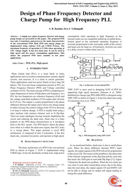
Fig. 1 Architecture <strong>of</strong> conventional PFD<br />
TSPC D-FF is more used in designing D-FF <strong>of</strong> PFD <strong>for</strong><br />
supporting high speed operation (Johnson et al, 2004).<br />
Modified pre-charge type PFD (MPt-PFD) is designed using<br />
TSPC-DFF as shown in Figure 2. It has free dead zone using<br />
16 transistors (Lee et al, 1999).<br />
Fig. 2 PFD designed by using TSPC D-FF<br />
III. DEAD ZONE<br />
As we mentioned be<strong>for</strong>e, dead-zone is due to small phase<br />
error. When the phase difference between PFD’s input<br />
signals, the output signals <strong>of</strong> the PFD will not be proportional<br />
to this error [10]. The reason <strong>of</strong> this problem is the delay time<br />
<strong>of</strong> the internal components <strong>of</strong> the flip-flop <strong>and</strong> the reset time<br />
that need s the AND gate to reset both flip flops [11]. Figure<br />
3 illustrates the dead zone problem. When the two clocks are<br />
very close to each other (small phase error), due to the delay<br />
time the reset delay, the output signals UP <strong>and</strong> DOWN will<br />
not be able to charge <strong>and</strong> no output will signal leading to<br />
losing this small difference.<br />
88
<strong>Design</strong> <strong>of</strong> <strong>Phase</strong> <strong>Frequency</strong> <strong>Detector</strong> <strong>and</strong> <strong>Charge</strong> <strong>Pump</strong> <strong>for</strong> <strong>High</strong> <strong>Frequency</strong> PLL<br />
error between Fclk <strong>and</strong> Fvco The conditions <strong>of</strong> inputs <strong>and</strong><br />
outputs are depicted in state machine diagram shown in fig<br />
6.<br />
TABLE I. LOGIC FUNCTIONS IMPLEMENTED WITH GDI CELL<br />
N P G D Functio<br />
n<br />
„0‟ B A A‟B F1<br />
Fig 3 : Dead Zone<br />
Figure 4 illustrates the output voltage vs. the phase error<br />
measured by the PFD. Figure.4a illustrates the relation in no<br />
dead zone PFDs, while figure 4b illustrates the relation in the<br />
presence <strong>of</strong> a dead zone. We can see that in a dead zone PFDs<br />
the relation become nonlinear around zero. This is due to<br />
inability to detect the phase error in this region. Plenty <strong>of</strong><br />
solution has been done <strong>for</strong> this problem some <strong>of</strong> them reduce<br />
the delay time in the internal components <strong>of</strong> the PFDs, other<br />
solution eliminate the reset path by implementing new reset<br />
techniques that will not create a delay <strong>and</strong> produce a high<br />
speed PFDs<br />
B „1' A A‟+B F2<br />
„1‟ B A A+B OR<br />
B „0‟ A AB AND<br />
C B A A‟B+A MUX<br />
C<br />
„0‟ „1‟ A A‟ NOT<br />
Figure 4: <strong>Phase</strong> Error vs. Output Voltage<br />
No Dead Zone (b) Dead Zone<br />
IV. PROPOSED PHASE FREQUENCY DETECTORS AND ITS<br />
SIMULATION RESULTS<br />
Fig 6 PFD state diagram<br />
The circuit diagram <strong>of</strong> proposed PFD is as shown in below<br />
figure 7 it works similar to conventional PFDs but it has<br />
many advantages compared to conventional PFDs. This<br />
PFDs is basically constructed with two GDI (Gate Diffusion<br />
Input) cells. A basic GDI cell contains four terminals – G<br />
(common gate input <strong>of</strong> nMOS <strong>and</strong> pMOS transistors), P (the<br />
outer diffusion node <strong>of</strong> pMOS transistor), N (the outer<br />
diffusion node <strong>of</strong> nMOS transistor), <strong>and</strong> D (common<br />
diffusion node <strong>of</strong> both transistors) . This technique allows<br />
reducing power consumption, propagation delay, <strong>and</strong> area <strong>of</strong><br />
digital circuits. The GDI method is based on the simple cell<br />
shown in Figure Table I shows how different logic functions<br />
implemented with GDI cell.<br />
Fig 7 Circuit diagram <strong>of</strong> the proposed PFD<br />
Fig 5 Basic GDI cell<br />
When Fclk is equal to Fvco both the outputs that is Up <strong>and</strong><br />
Down are zero, if Fclk is high compared to Fvco Then up<br />
signal is high else down signal is high indicating the phase<br />
Inputs(Fclk <strong>and</strong> Fvco) <strong>and</strong> outputs( Up <strong>and</strong> down) <strong>of</strong> the<br />
proposed logic at 5 GHZ is as shown in below fig 8. Outputs<br />
are verified according to the state machine diagram.<br />
89
International Journal <strong>of</strong> S<strong>of</strong>t Computing <strong>and</strong> Engineering (IJSCE)<br />
ISSN: 2231-2307, Volume-2, Issue-2, May 2012<br />
Fig 8 Input <strong>and</strong> output wave<strong>for</strong>ms <strong>of</strong> the proposed PFD<br />
V. FREQUENCY ANALYSIS<br />
The maximum operation frequency is defined as the<br />
shortest period with correct UP <strong>and</strong> DN signals together with<br />
the inputs have the same frequency <strong>and</strong> 90 degree phase<br />
difference [7]. A comparison <strong>of</strong> maximum operation<br />
frequency between conventional PFD, TSPC-PFD <strong>and</strong><br />
proposed PFD is shown in Figure 9. The comparison shows<br />
the variations <strong>of</strong> the maximum operation frequency with<br />
supply voltage. At 1.8V voltage supply the maximum<br />
operation frequency <strong>of</strong> the conventional PFD is 500 MHz, <strong>for</strong><br />
MPt-PFD is 1.5 GHz <strong>and</strong> proposed PFD is 4.5Ghz .This<br />
indicates that proposed PFD is reliable in high speed<br />
applications.<br />
Fig 10 Simulation results <strong>of</strong> the proposed PFD with a delay <strong>of</strong><br />
20ps<br />
VI. TEMPERATURE ANALYSIS<br />
Parametric analysis is done on PFD on variable temp the<br />
range is from 10 degrees to 100 degrees the analysis response<br />
is depicted in fig11. This indicates that proposed PFD is<br />
invariant with temperature. The delay <strong>of</strong> the proposed<br />
architecture is 19.71ns <strong>and</strong> is depicted in fig 12 This<br />
indicates that dead zone <strong>of</strong> the proposed architecture is<br />
approximately 20 ns <strong>and</strong> is much superior when compared<br />
with the conventional PFDs.<br />
Fig 9 Maximum operation frequency function <strong>of</strong> supply voltage<br />
<strong>for</strong> various PFDs<br />
Figure10 shows a longer simulation done on proposed PFD.<br />
The input CLK frequency is 500 MHz with Fclk leading Fvco<br />
by 20ps; this will result in having UP signal as we can see<br />
from the graph. This PFD were able to operate at much<br />
higher frequency 5GHZ is the highest frequency the PFD will<br />
operate at. Even at the phase difference <strong>of</strong> 20ps between Fclk<br />
<strong>and</strong> Fvco the proposed PFD is able to detect the difference<br />
which is depicted in fig10.<br />
Fig 11 PFD output wave<strong>for</strong>ms <strong>of</strong> parametric analysis <strong>for</strong> temperature<br />
ranging from 10 degrees to 100 degrees<br />
90
<strong>Design</strong> <strong>of</strong> <strong>Phase</strong> <strong>Frequency</strong> <strong>Detector</strong> <strong>and</strong> <strong>Charge</strong> <strong>Pump</strong> <strong>for</strong> <strong>High</strong> <strong>Frequency</strong> PLL<br />
Fig 12 Delay output<br />
Figure 13 shows the graph <strong>of</strong> the power measurement<br />
on <strong>and</strong> <strong>of</strong>f by the PFD output signals UP <strong>and</strong> DOWN. This<br />
charge pump consists <strong>of</strong> two switched current sources that<br />
pump charge into or out <strong>of</strong> the loop filter according to the<br />
PFD output. When the reference leads the feedback signal,<br />
the PFD detects a rising edge on the reference frequency <strong>and</strong><br />
it will produce an UP signal. This UP signal from the PFD<br />
will turn the UP switch (PMOS) on, <strong>and</strong> it will cause the CP<br />
to inject current into the loop filter, increasing Vout. When<br />
the feedback leads the reference signal, the PFD detects a<br />
rising edge on the feedback signal <strong>and</strong> will produce a DOWN<br />
signal. This DOWN signal from the PFD will turn the<br />
DOWN switch (NMOS) ON, <strong>and</strong> the CP will sink current out<br />
<strong>of</strong> the loop filter thus, decreasing Vout The current through<br />
the UP switch(PMOS), <strong>and</strong> the current through the DOWN<br />
switch(NMOS), need to be equal in order to avoid any<br />
current mismatch. The minimum charge pump current is<br />
limited by the switching speed requirements. Fig.15 shows<br />
the complete simulation result <strong>of</strong> phase detector with charge<br />
pump. It shows that the capacitor is charging only when the<br />
UP is high, <strong>and</strong> will be stable if the UP <strong>and</strong> DOWN both are<br />
low <strong>and</strong> vice versa.<br />
Fig13. Power measurement<br />
Fig 14 Circuit diagram <strong>of</strong> charge pump<br />
TABLE 2.PERFORMANCE COMPARISON BETWEEN DIFFERENT PFD<br />
TOPOLOGIES<br />
Sl<br />
noPFDs<br />
No <strong>of</strong><br />
transis<br />
tor<br />
Power<br />
consumpti<br />
on<br />
Maximum<br />
operating<br />
frequency<br />
Dea<br />
d<br />
zone<br />
Conventi<br />
onal<br />
48 33.5uW 500MHz 100p<br />
s<br />
T PFD 16 10uW 1.5GHZ 65ps<br />
Proposed 4 8uW 5GHz 20ps<br />
VII. CHARGE PUMP<br />
<strong>Charge</strong> <strong>Pump</strong> is the circuit that translates the UP <strong>and</strong><br />
DOWN signals from the PFD to control voltage that will<br />
control the VCO. As shown in Fig.14, charge pump consist<br />
<strong>of</strong> two switched current sources implemented using NMOS<br />
<strong>and</strong> PMOS diode connected load. <strong>Charge</strong> pump is switched<br />
Fig 15 Input <strong>and</strong> output wave<strong>for</strong>ms <strong>of</strong> charge pump<br />
91
VIII. LAYOUTS<br />
Fig 16 Layout <strong>of</strong> charge pump<br />
Both phase frequency detector <strong>and</strong> charge pump are<br />
implemented using cadence virtuoso 0.18um. Layout <strong>of</strong><br />
phase frequency detector <strong>and</strong> charge pump are depicted in fig<br />
16 <strong>and</strong> Fig 17.<br />
International Journal <strong>of</strong> S<strong>of</strong>t Computing <strong>and</strong> Engineering (IJSCE)<br />
ISSN: 2231-2307, Volume-2, Issue-2, May 2012<br />
4. Arshak, K., O. Abubaker, <strong>and</strong> E. Jafer, 2004. “<strong>Design</strong> <strong>and</strong> Simulation<br />
Difference Types CMOS <strong>Phase</strong> <strong>Frequency</strong> <strong>Detector</strong> <strong>for</strong> <strong>High</strong> Speed <strong>and</strong><br />
Low Jitter PLL”, proceedings <strong>of</strong> 5th IEEE International Caracas<br />
Conference on Devices, Circuits, <strong>and</strong> Systems, Dominican Republic,<br />
Vol. 1, Nov.3-5, pp.188-191.<br />
5. Johnson, T., A. Fard, <strong>and</strong> D. Aberg, 2004. “An Improved Low Voltage<br />
<strong>Phase</strong>-<strong>Frequency</strong> <strong>Detector</strong> with Extended <strong>Frequency</strong> Capability”, The<br />
47th IEEE International Midwest Symposium on Circuits <strong>and</strong> Systems,<br />
pp. 181-184.<br />
6. Lee, G. B., P. K. Chan, <strong>and</strong> L. Siek, 1999.“A CMOS <strong>Phase</strong> <strong>Frequency</strong><br />
<strong>Detector</strong> <strong>for</strong> <strong>Charge</strong> <strong>Pump</strong> <strong>Phase</strong>-Locked loop”, IEEE 42nd Midwest<br />
Symposium on Circuits <strong>and</strong> Systems, Vol.2, pp. 601 – 604.<br />
7. Kondoh, H., H. Notani, T. Yoshimura, H. Shebata, <strong>and</strong> Y. Matsuda, 1995.<br />
“A 1.5-V 250-MHz to 3-V 622-MHz operation CMOS <strong>Phase</strong>-Locked<br />
Loop with Precharge type <strong>Phase</strong> <strong>Detector</strong>”, IEICE Trans. Electron, Vol.<br />
E78-C, no.4, pp 382-388.<br />
8. Razavi, 2003.“<strong>Design</strong> <strong>of</strong> Integrated Circuits <strong>for</strong> Optical Communications”,<br />
McGraw-Hill, USA.<br />
9. El-Hage, M., <strong>and</strong> F. Yuan, 2003. “ Architectures <strong>and</strong> <strong>Design</strong> Consideration<br />
<strong>of</strong> CMOS <strong>Charge</strong> <strong>Pump</strong> <strong>for</strong> <strong>Phase</strong>-Locked Loops”, Electrical <strong>and</strong><br />
Computer engineering, IEEE CCECE Canadian Conference, ON, Vol.<br />
1, pp. 223 – 226.<br />
10. Barrett, Curtis. Fractional/Integer-N PLL Basics. Texas Instruments,<br />
Wireless Communication Business Unit, August 1999.<br />
11. Chou, Chien-Ping, Lin, Zhi-Ming,<strong>and</strong> Chen, Jun-Da. “<br />
A 3-PS Dead-Zone Double- Edge-checking<br />
<strong>Phase</strong>-<strong>Frequency</strong>-<strong>Detector</strong> With 4.78 GHz Operation<br />
<strong>Frequency</strong>.” The 2004 IEEE Asia-Pacific Conference on<br />
Circuits <strong>and</strong> Systems conference. (2004) : Volume 2,<br />
Page(s): 937 – 940.<br />
S B Rashmi received her BE. Degree in Electronics <strong>and</strong> communication from<br />
visveswaraya Technological Universi-ty, Karnataka, India in 2004. She is<br />
currently perusing her M Tech. in VLSI <strong>and</strong> Embedded systems from VTU,<br />
Karna-taka India. She is a member <strong>of</strong> IEEE <strong>and</strong> IACSIT. She was awarded best<br />
student paper award in the “Knowledge Utsav Conference on Communication<br />
Technologies <strong>and</strong> VLSI design, Jain University, Karnataka, India.” Her areas <strong>of</strong><br />
research interest are reversible logic design, quantum cryptography <strong>and</strong> Low<br />
power VLSI<br />
Fig 17 Layout <strong>of</strong> phase frequency detector<br />
Dr. Siva Yellampalli obtained his MS & Ph.D from Louisiana State<br />
University. He is currently with VTU Extension Centre, UTL Technologies Ltd.<br />
He worked on a broad range <strong>of</strong> research topics including Very Large Scale<br />
Integration (VLSI), mixed signal circuits/systems development,<br />
micro-electromechanical systems (MEMS), <strong>and</strong> integrated carbon nanotube<br />
based sensors. He has published a book, multiple Journal papers <strong>and</strong> IEEE<br />
Conference papers in these areas <strong>of</strong> research. He also edited two books in the<br />
area <strong>of</strong> carbon nanotubes. In addition he has given many pr<strong>of</strong>essional<br />
presentations including invited talks. He has been a consultant to a variety <strong>of</strong><br />
industries <strong>and</strong> acts as a reviewer <strong>for</strong> technical journals <strong>and</strong> book publishers. He<br />
is a life member <strong>of</strong> Indian Society <strong>for</strong> Technical Education (ISTE), senior<br />
member, International Association <strong>of</strong> Computer Science <strong>and</strong> In<strong>for</strong>mation<br />
Technology (IACSIT) <strong>and</strong> member <strong>of</strong> IEEE, VLSI Society <strong>of</strong> India (VSI) <strong>and</strong><br />
National Society <strong>of</strong> Collegiate Scholars (NSCS).<br />
IX. CONCLUSIONS<br />
This paper presents new PFD <strong>and</strong> charge pump design<br />
implemented using cadence 0.18 μm CMOS process. PFD is<br />
composed <strong>of</strong> 4 transistors, <strong>and</strong> preserves the main<br />
functionality <strong>of</strong> a conventional PFD. The circuit operates at a<br />
frequency <strong>of</strong> 5 GHZ with dead zone <strong>of</strong> 20ps<br />
.<br />
REFERENCES<br />
1. A Simple CMOS PFD <strong>for</strong> <strong>High</strong> Speed Applications Nesreen Ismail Institute<br />
<strong>of</strong> Micro-Engineering <strong>and</strong> Nano-Electronics University Kebangsaan<br />
Malaysia, MalaysiaMasuri Othman Institute <strong>of</strong> Micro-Engineering <strong>and</strong><br />
Nano-Electronics University Kebangsaan Malaysia, Malaysia<br />
2. Leenaerts, D., J. V. D. Tang, <strong>and</strong> C. S. Vaucher, 2001. “Circuit <strong>Design</strong> <strong>for</strong><br />
RF Transceivers”,Kluwer Academic Publishers, USA, pp. 243-258.[2]<br />
Best, R. E., 1993. “<strong>Phase</strong>-Locked Loop <strong>Design</strong>, Simulation, <strong>and</strong><br />
Application”, 2nd edition,McGraw Hill, New York.<br />
3. Johansson, H., 1998. “Simple Precharged CMOS <strong>Phase</strong> <strong>Frequency</strong><br />
<strong>Detector</strong>”, IEEE Journal <strong>of</strong> solid state circuits, Vol. 33, No. 2, pp.<br />
295-299.<br />
92