Technology - Sumitomo Electric Industries, Ltd.
Technology - Sumitomo Electric Industries, Ltd.
Technology - Sumitomo Electric Industries, Ltd.

Create successful ePaper yourself
Turn your PDF publications into a flip-book with our unique Google optimized e-Paper software.
Head Office (Osaka)<br />
5-33, Kitahama 4-chome, Chuo-ku, Osaka 541-0041, Japan<br />
Tel: +81 6 6220 4141<br />
http://global-sei.com/<br />
March 2012
R&D organization<br />
Business segments and<br />
creation of new products<br />
R&D General Managing Unit<br />
New business segments<br />
(Environment & Resources, Life Sciences,<br />
Safety/Security/Ubiquitous Networking)<br />
Five existing business segments<br />
<strong>Electric</strong> Wire & Cable, Energy<br />
<strong>Technology</strong><br />
R&D General<br />
Planning Division<br />
Semiconductor<br />
Technologies<br />
R&D Laboratories<br />
P18<br />
Analysis <strong>Technology</strong><br />
Research Center<br />
P10<br />
New Business Frontier<br />
R&D Laboratories<br />
P04 P05 P08<br />
Materials and<br />
Processs<br />
<strong>Technology</strong> R&D Unit<br />
Electronics &<br />
Materials R&D Laboratories<br />
Power System<br />
R&D Laboratories<br />
Automotive<br />
<strong>Technology</strong><br />
R&D Laboratories<br />
P12<br />
Industrial Materials<br />
and Process <strong>Technology</strong><br />
R&D Laboratories<br />
P16<br />
Electronics<br />
Information & Communications<br />
Automotive<br />
Industrial Materials<br />
R&D General<br />
Planning Division<br />
Marketing<br />
R&D Planning<br />
Exploration/Surveys<br />
Technical management<br />
Human resource<br />
development<br />
Analysis <strong>Technology</strong><br />
Research Center<br />
Analysis and evaluation<br />
CAE analysis<br />
New Business Frontier<br />
R&D Laboratories<br />
Automotive <strong>Technology</strong><br />
R&D Laboratories<br />
Lifescience Business Development Department<br />
Compovision ®<br />
Water Business Development Department<br />
‘‘Ecomarine TM ’’ ballast water management system<br />
Desalination pretreatment system (TT unit)<br />
Agriculture Business Development Department<br />
Nutrient Culture System<br />
HEV/EV motor components<br />
HEV/EV reactors<br />
Automotive PLC unit<br />
High-temperature superconducting motor<br />
Power System R&D<br />
Laboratories<br />
Concentrator photovoltaic<br />
Battery energy storage system<br />
Power conditioner<br />
Distributed electric power system<br />
High-temperature superconducting tape<br />
Industrial Materials and Process <strong>Technology</strong><br />
R&D Laboratories<br />
High-Strength Magnesium<br />
Alloy Sheet and its application<br />
High performance cemented carbide<br />
and cermet cutting tools<br />
CVD, PVD coating and its application products<br />
High-performance cBN tool,<br />
nano-polycrystalline diamond tool<br />
Low-Iron-Loss Soft Magnetic<br />
Powder Cores and Applications<br />
High Strength P/M Aluminum<br />
Alloy and Applications<br />
High Strength Steel Wires<br />
for Valve Springs<br />
High Strength Saw Wires<br />
Optical Ceramincs for<br />
laser material processing<br />
High thermal conductivie<br />
AlN ceramics and its application<br />
Innovation Core<br />
SEI, Inc.<br />
P27<br />
Overseas operations<br />
ons<br />
P14<br />
P20<br />
Information andCommunications<br />
<strong>Technology</strong> R&D Unit<br />
Transmission<br />
Devices<br />
R&D Laboratories<br />
P22<br />
Information &<br />
Communications<br />
Laboratories<br />
Optical<br />
Communications<br />
R&D Laboratories<br />
P24<br />
Semiconductor Technologies<br />
R&D Laboratories<br />
Compound semiconductors and devices<br />
Crystal growth characterization technology<br />
Information & Communications<br />
Laboratories<br />
Optical access system<br />
Wireless access system<br />
IP terminals<br />
Road traffic systems<br />
Safety & Security,<br />
Ubiquitous Networking<br />
Image/Radio frequency sensors<br />
Electronics & Materials R&D Laboratories<br />
Transmission Devices<br />
R&D Laboratories<br />
Flexible printed circuits<br />
Anisotropic conductive film<br />
High speed flat transmission cable<br />
Micro flex coaxial cables and harnesses<br />
Environmentally friendly battery materials<br />
Metallic nano-pastes & links<br />
Optical communication devices<br />
Optical communication modules<br />
Next generation transmission technologies<br />
Optical communication data links<br />
Wireless communication devices<br />
Polymer nano-composite based heat-shrinkable tubes<br />
SUMI-CARD with innovative functions<br />
Next-generation magnet wire<br />
Insulation material technology for high-voltage power cable<br />
Heat spreader materials<br />
Molten salt electrolysis batteries<br />
Optical Communications<br />
R&D Laboratories<br />
High capacity transmission fiber<br />
Low bending loss fiber<br />
Optical modules for optical nodes<br />
Optical interconnection technology<br />
High-power optic applications<br />
02 03
R&D General<br />
Planning Division<br />
New Business<br />
Frontier R&D Laboratories<br />
The R&D General Planning Division, concurrently part of both R&D Units, specially<br />
handles tasks common to the Company’s R&D activities, mainly in the areas of research<br />
planning, management and assistance.<br />
Research planning<br />
To enhance R&D activities of individual Laboratories, we investigate and analyze information external to the <strong>Sumitomo</strong> <strong>Electric</strong> Group<br />
that relates to advanced technologies, market and competition trends, etc. We comply and classify information on core technologies<br />
and other resources internal to the <strong>Sumitomo</strong> <strong>Electric</strong> Group, so as to promote optimal utilization of our technologies. We also explore<br />
and develop new research themes. We encourage collaboration between Laboratories and external research institutions, as well as<br />
Laboratories’ participation in government-funded projects, so as to promote R&D activities that optimally utilize external resources.<br />
Research management<br />
We manage overall pursuit of the R&D Group's research activities by supervising projected and actual budgets, personnel arrangements<br />
and research achievements; reporting R&D Group activities to management; and communicating management policies to the Laboratories.<br />
Lifescience Business Development Department<br />
The Lifescience Business Development Department promotes product development in<br />
the life science field, based on <strong>Sumitomo</strong> <strong>Electric</strong>’s core technologies.<br />
Our activities presently center around the development and commercialization of<br />
Compovision ® , a compositional imaging system making use of the characteristics of near<br />
infrared light. We intend to develop a variety of products in the future.<br />
Development of Compovision ®<br />
We work on the development of Compovision ® , which, using optical communications devices and material technologies, renders<br />
two-dimensional images of material composition and concentration distribution in real time in a nondestructive and contactless<br />
manner. Compovision ® serves as an inspection system for safety and quality control of products and materials. With this imaging<br />
system, <strong>Sumitomo</strong> <strong>Electric</strong> aims to gain a substantial market share of the pharmaceutical and food industries.<br />
We also promote activities of individual research project teams through progress analysis, advice in research planning, formation of organizational<br />
units appropriate to different development stages, and allotment of human resources. We control budget implementation relating<br />
to projects using external funds, including national government-led projects. We conduct human resource development for the entire<br />
R&D Group, formulate regulations concerning compliance, information management, etc. and provide relevant education to researchers.<br />
Optical Communications<br />
R&D Laboratories<br />
NewBusinessFrontierR&DLaboratories/<br />
Lifesciece BusinessDevelopment Department<br />
Development of near<br />
infrared light source<br />
(SC light source)<br />
Development of<br />
near infrared camera<br />
Transmission Devices R&D Labs./<br />
Semiconductor Technologies R&D Labs.<br />
Research assistance<br />
To assist the Laboratories in their research activities, we maintain a staff of research assistants, manage them, supervise their duties<br />
and assignments, maintain and control research facilities, equipment, materials, etc.<br />
R&D expenses (including development expenses at production groups)<br />
Development of<br />
highly nonlinear fiber<br />
Development of<br />
near infrared sensor<br />
100<br />
¥bn<br />
80<br />
60<br />
40<br />
723<br />
37.5<br />
790<br />
45.1<br />
850<br />
49.0<br />
Business Unit Market Trend Key <strong>Technology</strong>/Activity<br />
Automotive<br />
Information &<br />
Communications<br />
Electronics<br />
Environmental (HEV/EV)<br />
Light weight<br />
Safety<br />
Comfort<br />
Capa increase in trunk line,<br />
FTTH, Wireless access,<br />
High speed wiring, Opticalwiring,<br />
Net working of domestic appliances,<br />
Safety, Energy saving,<br />
Power device<br />
Compact, High density,<br />
Light weight,<br />
Energy saving<br />
Aluminum WH, FineCu-SUSWH,<br />
High voltage WH for HEV/EV, Booster circuit parts,<br />
Next generation automotive LAN,<br />
Solid Libattery, Electronic control unit,<br />
Automotivepower distributor<br />
High speed link/module, GaN electronic device,<br />
Photonic NW module, Optical wiring,<br />
Next generation optical fiber for trunk line,<br />
Applied optical power, Optical & wireless access,<br />
IP unit, Appliance for image distribution,<br />
ITS wireless appliance, Sensor technology for<br />
image and radio wave, SiC power device<br />
High performance FPC, High density parts &<br />
materials, Tab-lead for automotive,<br />
Metal nanoparticle, Large GaN substrate,<br />
Green GaN laser, GaN power device,<br />
Next generation semiconductor material<br />
Information &<br />
Communications Labs.<br />
Development of<br />
identification algorithm<br />
Development of<br />
spectral database<br />
20<br />
0<br />
17.5 17.1<br />
16.0<br />
5.0<br />
5.6 5.4<br />
7.6 7.2<br />
9.5<br />
4.1 4.2 5.5<br />
2009 2010 2011 E<br />
<strong>Electric</strong> Wire,<br />
Cable & Energy<br />
Industrial<br />
Materials<br />
Energy saving,<br />
Environmental,<br />
Paradigm shift of energy,<br />
Battery<br />
High accuracy machining,<br />
High performance<br />
automotive parts,<br />
Rare material measures<br />
High temperature superconducting wirecablecoil,<br />
electricity controlling apparatus,<br />
Solar power generation, RF battery,<br />
Molten-salt battery, Aluminum celmet,<br />
High voltage insulating technology, HV coil<br />
High performance tooling materials<br />
(Hardmetal, Diamond, CBN),<br />
High performancemagnetic powder, Magnesium alloy,<br />
High performance special steel wire,<br />
Infrared optical material, Tungsten recycling technology<br />
Development of Compovision ® Development of inspection/<br />
diagnostic system<br />
User (food plants, pharmaceutical factories, etc.)<br />
04 05
New Business Frontier R&D Laboratories<br />
Applications of Compovision ®<br />
Compovision ® reveals slight compositional changes and<br />
differences in two-dimensional images. Its application<br />
examples include the following:<br />
Quantitative protein inspection<br />
Protein denaturation inspection<br />
Fatty acid inspection<br />
Moisture inspection<br />
Foreign matter (hair, etc.) determination<br />
Fat distribution measurement<br />
Hair determination example<br />
Image by<br />
Compovision ®<br />
Visible-light image<br />
White hair<br />
Black hair<br />
Dyed hair<br />
Fatty acid reflection spectrum analysis results (each sample size: n = 4)<br />
Visible-light<br />
image<br />
Heavy Light<br />
Treatment temp.<br />
Acid A A<br />
Image by<br />
Compovision ®<br />
(Moisture content)<br />
High<br />
Acid M<br />
Low<br />
Image by<br />
Compovision ®<br />
(Protein denaturation)<br />
Acid K<br />
Acid C<br />
Acid B<br />
Acid D<br />
Acid H<br />
Acid E<br />
Measurements in a broad band of wavelengths from<br />
1,000 to 2,350 nm enable identification of some 10 fatty acids.<br />
Acid F F<br />
Acid G<br />
Examples of the moisture content of heated cheese and protein denaturation<br />
Water Business Development Department<br />
We work on the development of water treatment system to contribute to improving<br />
global water shortage and water environment issues based on our unique polytetrafluoroethylene<br />
(PTFE) membrane technology in combination with ideas created from flexible<br />
mindsets.<br />
‘‘Ecomarine TM ’’ ballast water management system<br />
We successfully developed the ‘‘Ecomarine TM ’’ ballast water management system that is simply composed of filter and UV units<br />
applicable to high-turbidity seawater to address aquatic organisms in ballast water discharged from ships that have grown in foreign<br />
marine environments and caused environment issues.<br />
The ‘‘Ecomarine TM ’’ is an energy-saving and eco-friendly system that removes large aquatic organisms with filter and eliminates<br />
small ones with UV without need for chemicals.<br />
Intake sea water<br />
Seawater<br />
intake<br />
P<br />
Pump<br />
Seawater<br />
Treated<br />
water<br />
1Removal of large<br />
plankton<br />
Filter unit<br />
Filter unit<br />
Ballast water<br />
2Sterilization by<br />
uitraviolet irradiation<br />
Ballast water tank<br />
Ultraviolet system<br />
Untreated seawater<br />
discharged<br />
This example illustrates the detection of white,<br />
black and dyed hair placed against a white background.<br />
(Hair portions indicated in red)<br />
These examples show subtle changes in the moisture content<br />
of heated cheese and in protein denaturation.<br />
Agriculture Business Development Department<br />
Drain ballast water<br />
Filter unit<br />
Filter unit<br />
Sterilization by<br />
ultraviolet irradiation<br />
Ultraviolet system<br />
Based on our nutrient culture system we have developed for years, Agriculture Business<br />
Development Department aims at stable supply of vegetables and other plants through<br />
industrially-managed production.<br />
P<br />
Pump<br />
Ballast water<br />
Ballast water tank<br />
Treated water<br />
drained<br />
Nutrient Culture System<br />
Products<br />
Fertigation<br />
Controller<br />
(Water Source)<br />
Liquid Fertilizer<br />
Dilution Unit<br />
Drip Fertigation<br />
Tube<br />
Fertigation<br />
Control Unit<br />
Sandculture Bed<br />
Butter Lettuce<br />
Grape Tomato<br />
Desalination pretreatment system (TT unit)<br />
Seawater Desalination System<br />
Conventional<br />
System<br />
Hypochlorous<br />
acid<br />
Intake<br />
Pretreatment<br />
Iron chloride<br />
Pond<br />
TT Unit<br />
under development<br />
Intake<br />
Primary<br />
filtration<br />
Sand filter<br />
Secondary<br />
filtration<br />
Sand filter<br />
MF, UF membrane<br />
TT Unit<br />
Sulfuric acid<br />
Sodium bisulfite<br />
Sulfuric acid<br />
Security filter<br />
Security filter<br />
Desalination<br />
RO<br />
membrane<br />
RO<br />
membrane<br />
Removing turbidity efficiently<br />
Reducing chemical use<br />
Seawater desalination is expected to significantly grow in<br />
demand due to global water shortage. The challenge is that<br />
jellylike transparent exo-polymer particles (TEP) in seawater<br />
cause a dramatic reduction in membrane permeability.<br />
We developed the desalination pretreatment system (TT unit) that<br />
is composed of TEP Trap (TT) membrane to remove TEP<br />
efficiently in combination with cleaning mechanism.<br />
This system allows the treatment at higher flow rate compared to<br />
conventional pretreatment membrane and the dramatic reduction<br />
in needed membrane area and treatment cost.<br />
06 07
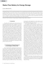
Power System<br />
R&D Laboratories<br />
Redox flow battery<br />
Renewable energy power sources<br />
Power generating facilities and devices<br />
(solar, wind power, etc.)<br />
<strong>Electric</strong> power system<br />
and electric power plant NW<br />
Power generation<br />
Control center<br />
Wind and solar power<br />
Power transmission<br />
Devices/control technology to stabilize electric power systems<br />
Energy saving devices and electric power monitoring/control technology<br />
SiC inverter<br />
HEMS, DSM, DR and Home NW<br />
Interface with electrical load products<br />
V2G system<br />
Large load<br />
(air conditioners,<br />
refrigerators, etc.)<br />
to supply<br />
side<br />
Transformation<br />
Monitor<br />
Heat pump<br />
Water heater<br />
Storage<br />
battery<br />
Next-generation power transmission/distribution network (new cables/transmission lines, DC power transmission, superconductivity)<br />
Stabilizing devices (storage batteries, transformers, SVC, preventing isolated operation, etc.)<br />
Automated, system operating system<br />
Server<br />
Distribution<br />
Consumption or<br />
distributed power sources<br />
s<br />
The Power System R&D Laboratories newly opened in<br />
January 2010 to promote business development in line<br />
with technological innovations in the electric power infrastructure<br />
sector (such as expanded use of renewable energies<br />
and advanced electric power infrastructure using information<br />
and communications technology). More specifically,<br />
the laboratories promote research and development of<br />
elemental technologies, commercial products, equipment<br />
and systems that are essential for smart grid construction.<br />
In a power system using power generated by renewable energy, the storage<br />
battery plays the critical role of storing and discharging electric power<br />
in response to fluctuations in generated electric power. Redox flow batteries<br />
are suitable for irregular, highly fluctuating charge/discharge operations,<br />
enabling accurate monitoring and control of stored electric power.<br />
Accordingly, they are optimal storage batteries for smart grids designed for<br />
efficient use of solar, wind power and other renewable energy resources.<br />
We are focusing product development efforts on redox flow batteries for<br />
use in smart grids on a fully commercial basis.<br />
Power conditioner and POWER DEPO TM storage battery system<br />
Micro smart-grid demonstration system<br />
(Left) A PV inverter converts generated DC power to AC power. Provided<br />
with voltage control and communications functions, it also<br />
Display/<br />
operation terminal<br />
DC power<br />
AC power<br />
Information<br />
Photovoltaic<br />
DC/DC<br />
Converter コンバータ<br />
Smart distributor<br />
Small wind turbine<br />
DC/DC<br />
Converter コンバータ<br />
Inverter<br />
Intelligent tap<br />
Redox flow battery<br />
Bi-Directional DC/DC<br />
Converter コンバータ<br />
EV charging station<br />
Concentrator photovoltaic<br />
DC/DC<br />
Converter コンバータ<br />
We have developed a micro smart-grid demonstration<br />
system and have been testing it at our Osaka Works. Four<br />
types of renewable power generators and a storage battery<br />
are DC-interconnected, and natural energy and power<br />
demand fluctuations are sophisticatedly managed, thereby<br />
ensuring stable and efficient power supply for facilities and<br />
equipment (loads).<br />
Smart distributor and intelligent tap<br />
We also develop devices that support<br />
power usage visualization equipment<br />
Energy<br />
management<br />
server<br />
resolves natural energy problems such as fluctuations in output<br />
power.<br />
(Right) Prototype of POWER DEPO TM storage battery system<br />
Central control server (EMS server)<br />
Concentrator photovoltaic<br />
Superconductor electric vehicle<br />
and demand response required by the<br />
EMS (energy management system),<br />
such as smart distributors and intelligent<br />
taps.<br />
Internet<br />
Smart distributor<br />
Intelligent tap<br />
The power generation efficiency of concentrator photovoltaic<br />
(CPV) is about twice that of silicon solar panels currently<br />
on the market, since CPV cells are made from a special<br />
compound semiconductor material. By being installed<br />
at an elevated position, concentrator panels provide usable<br />
space underneath them. Expectations are high for CPV as a<br />
next-generation photovoltaic. In the newly developed CPV<br />
(1 kW power), panels are thinner and lighter than those of<br />
conventional CPV.<br />
Superconducting tape<br />
Bismuth-based superconductors have moved from the research phase to commercialization,<br />
with development work being promoted by the Superconductivity <strong>Technology</strong> Division.<br />
Home gateway<br />
<strong>Sumitomo</strong> <strong>Electric</strong> developed the world’s first, weak magnetic, high<br />
strength, textured metal substrate. A buffer layer and an yttriumbased<br />
superconducting layer are deposited on this substrate in<br />
sequence by sputtering and pulsed laser deposition, respectively.<br />
This superconducting wire exhibits 3 MA/cm 2 or higher critical current<br />
that is applicable for practical use.<br />
08 09
Analysis <strong>Technology</strong><br />
Research Center<br />
3D structure visualization<br />
The Analysis <strong>Technology</strong> Research Center supports the <strong>Sumitomo</strong> <strong>Electric</strong> Group’s<br />
manufacturing, product development, business development and technological foundation.<br />
The Center is active at three sites, in Osaka, Itami and Yokohama, uses advanced<br />
large research facilities (SPring-8, Earth Simulator, etc.) outside the Company, and<br />
boasts sophisticated analysis techniques and computer aided engineering (CAE).<br />
Strategic CAE infrastructure development<br />
Microfocus X-ray CT system<br />
Dual focused-ionbeam<br />
machining<br />
and observation system<br />
3D observation of internal strand structure of multicore cable<br />
IC device internal structure<br />
Continuous observation of<br />
FIB-machined cross sections<br />
3D rendering<br />
Three-dimensional structure visualization has been developed<br />
for composite materials, parts and products to reveal:<br />
・internal structures<br />
・desired specific areas<br />
・objects as they are<br />
This technology is useful for improving product quality and<br />
developing solutions to problems.<br />
Yokohama<br />
General computation server<br />
IBM System p570<br />
CPU: 16-core, 4.7 GHz clock speed<br />
Memory: 384 GB<br />
IBM Blade Center HS22<br />
・INTEL Xeon X5570 2.93GHz<br />
128CPU(8CPU×16Nodes)<br />
High-speed networks<br />
In-house<br />
Affiliates<br />
Itami<br />
General computation server<br />
The use of CAE is not simply intended to improve product<br />
development efficiency. We regard it as a key technology<br />
for attaining increased market competitiveness. Our efforts<br />
are directed toward infrastructure development to enhance<br />
the core CAE functionality of the <strong>Sumitomo</strong> <strong>Electric</strong> Group.<br />
Elemental mapping with sub-micron resolution<br />
We work on the development of a technology to visualize,<br />
with high spatial resolution, the distribution of a lowconcentration<br />
dopant that determines the characteristics of<br />
functional materials and parts, using an electron probe<br />
microanalyzer.<br />
Electron probe<br />
microanalyzer<br />
Elemental mapping of sintered aluminum nitride<br />
Impurity deposits at<br />
grain boundaries<br />
(1μm)<br />
SEM image<br />
High<br />
Crystal grain<br />
boundary<br />
Crystal<br />
grain<br />
Low<br />
For widespread use of CAE for analytical purposes<br />
Nanometer-level structural analysis<br />
Power cable accessories<br />
and analysis example<br />
Required time (day)<br />
Automated system<br />
6<br />
Result processing<br />
5<br />
Computation<br />
Mesh generation<br />
4<br />
3<br />
Analysis time reduced to one-fifth<br />
2<br />
1<br />
0<br />
Conventional method Automated system<br />
We promote the development and widespread use of CAE<br />
analysis techniques that are useful for product designing.<br />
Our efforts include providing training to designers and<br />
developing simplified/automatic analysis systems. Thus, we<br />
work on the transfer of analysis techniques to design<br />
departments using procedures that precisely meet designers’<br />
needs.<br />
EDX detector<br />
Characteristic<br />
X-ray<br />
Thin-film<br />
specimen<br />
High-angle<br />
scattered<br />
electrons<br />
Transmitted<br />
electrons<br />
Incident electrons<br />
SE/BSE detector<br />
Secondary/<br />
Back-scattered electron<br />
Probe diameter: 0.1 nm<br />
Annular dark-field detector<br />
(HAADF)<br />
Bright-field detector<br />
Scanning transmission<br />
electron microscope (STEM)<br />
Si [110] dumbbell structure<br />
Si crystal model<br />
Our efforts are directed toward developing a nanometerlevel<br />
structural analysis technology in order to establish an<br />
analytical technology and its applications, principally using<br />
scanning transmission electron microscopes and conducting<br />
crystal structure analyses.<br />
<strong>Electric</strong> wire service life prediction<br />
Analysis on the atomic scale using synchrotron radiation and first-principles calculation<br />
<br />
<br />
<br />
<br />
<br />
<br />
<br />
<br />
<br />
<br />
<br />
<br />
<br />
<br />
<br />
<br />
<br />
Mobile phone hinges, automotive doors and robot arms<br />
have electric wires and cables installed in their moving<br />
parts. We work on the development of a computer simulation<br />
technology for predicting the service life of such wires<br />
and cables until breakage due to twisting and bending.<br />
We work on technological development such as structural<br />
analysis of materials at the atomic scale and in-situ reaction<br />
analysis, using synchrotron radiation and neutrons.<br />
Moreover, our aims include elucidation of characteristic<br />
development mechanisms and exploration of new materials,<br />
in which the aforementioned technology is combined<br />
with first-principles calculation and other simulations.<br />
Large synchrotron radiation facility (SPring-8)<br />
Electrons revolve in<br />
storage ring 500 m in diameter.<br />
Courtesy:<br />
Japan Synchrotron<br />
High-intensity<br />
Radiation Research Institute<br />
X-rays<br />
Earth Simulator<br />
Courtesy:<br />
Japan Agency for Marine-<br />
Earth Science and <strong>Technology</strong><br />
Radial distribution function<br />
Structural analysis example<br />
(Er-doped optical fiber)<br />
Measurement by SPring-8 X-rays<br />
Molecular dynamics simulation<br />
Interatomic distance (nm)<br />
10 11
Automotive <strong>Technology</strong><br />
R&D Laboratories<br />
Power electronics technology<br />
Our mission is to conduct research in the automotive field by applying core material<br />
technologies of <strong>Sumitomo</strong> <strong>Electric</strong>, and to develop modules for future automotive products<br />
in collaboration with other laboratories.<br />
<strong>Sumitomo</strong> <strong>Electric</strong> Group Automotive Products<br />
Gateway<br />
Engine<br />
Motor<br />
Magnet wire<br />
Inverter<br />
Gateway<br />
Converter<br />
Reactor<br />
Charger<br />
AC-DC<br />
converter<br />
Reactor<br />
Battery<br />
Reactor<br />
<strong>Sumitomo</strong> <strong>Electric</strong> has the key component materials and<br />
design technology for HEV/P-HEV/EV power modules. We<br />
are currently developing reactors and converters that are<br />
smaller and lighter than existing products.<br />
Vehicle communication technology<br />
Ensuring standardized communication between vehicle and<br />
Fast<br />
charge<br />
AC<br />
charge<br />
Wiring harnesses<br />
High-voltage power cables<br />
Sintered materials<br />
charging station (vehicle-to-grid communication) is an<br />
important issue. Therefore, ISO, IEC and SAE are in the<br />
process of setting international standards for vehicle-to-grid<br />
Cable<br />
communication. <strong>Sumitomo</strong> <strong>Electric</strong> has joined with ISO, IEC<br />
and SAE, in leading the activities of JARI/JSAE in Japan.<br />
Charging stand<br />
Communication<br />
Standardization:<br />
EU:ISO/IEC<br />
USA:SAE<br />
Japan:JARI/JSAE<br />
Anti-vibration rubbers<br />
Reactor<br />
(in development)<br />
Evaluation/Analysis technologies<br />
<strong>Sumitomo</strong> <strong>Electric</strong> has proprietary technologies for electromagnetic<br />
analysis and thermal analysis that are based on<br />
Connectors<br />
Super conducting motor<br />
(in development)<br />
Magnet wires<br />
Dust core<br />
CAE analysis<br />
Coil<br />
computer aided engineering (CAE). We also have evaluation<br />
technology with bench tests. Therefore, we are able to<br />
develop automotive products with these design, materials,<br />
assembly and evaluation technologies.<br />
Automotive technology development<br />
High-temperature superconducting motor<br />
ATL is developing new technologies and new products as a<br />
core member of an ABC (automotive business committee),<br />
which is a cross-functional organization working in collaboration<br />
with other automotive sections to correspond to the<br />
paradigm shift in vehicle design.<br />
Sensor<br />
Traffic control<br />
Gateway<br />
Engine<br />
Magnet Coil<br />
Motor<br />
Magnet wire<br />
ITS system<br />
Vehicle<br />
information Information<br />
LAN<br />
Inverter<br />
SiC<br />
Heat sink<br />
Telematix<br />
Wireless power transfer<br />
Gateway<br />
ECU<br />
W/H<br />
Traffic<br />
information<br />
Converter<br />
reactor<br />
Smart grid<br />
Connector<br />
AC-DC converter<br />
Charger<br />
PLC unit<br />
Battery<br />
<br />
In order to improve battery efficiency and to extend the<br />
range of electric vehicles, we are working on the development<br />
of high efficiency superconducting motor. We have<br />
succeeded in the development of the world's first electric<br />
vehicle equipped with a superconducting motor and a<br />
cryocooler that can greatly improve the ease of maintenance.<br />
12 13
Electronics & Materials<br />
R&D Laboratories<br />
2<br />
Polymer Meterials Technologies<br />
Supporting the fundamental<br />
technologies of SEI<br />
1 Metals & Inorganic Materials <strong>Technology</strong><br />
Metals &<br />
Inorganic<br />
Materials<br />
<strong>Technology</strong><br />
Wiring &<br />
Connection<br />
Technologies<br />
Polymer<br />
Meterials<br />
Technologies<br />
Total<br />
enhancement<br />
of core tech.<br />
Insulating material for<br />
electronics & electric<br />
cables<br />
Nano composite<br />
Polymer<br />
alloy<br />
Compatibilizer<br />
Miscible to<br />
Polymer A<br />
Polymer alloy<br />
Polymer alloy<br />
Miscible to<br />
Polymer B<br />
Halogen free materials<br />
Polymer A<br />
Polymer B<br />
Electronic <br />
Business<br />
contribution<br />
Heat shrincable tub<br />
Tech. of Metals<br />
Tech. of polymer synthesis<br />
& compounding<br />
Super high voltage power cable<br />
Magnetic wire for HV<br />
Molecular design<br />
Polymer synthesis<br />
Optical cable<br />
Functional<br />
polymer<br />
Polymer synthesis<br />
Synthesis of<br />
adhesive<br />
Wiring harness using aluminum wires<br />
Continuous casting<br />
Plastic forming<br />
Material designing<br />
Al-SiC heat-spreader<br />
Composite material(metal/ceramics)<br />
3<br />
Wiring & Connection Technologies<br />
Photosensitive polymer<br />
Flexible printed circuit<br />
Application of plating<br />
Synthesis & application of metal nano particles<br />
Ag nano particles Cu nano particles Chainlike Ni nano particles<br />
Anisotropic Conductive Film(ACF)<br />
Mobile devicesPC<br />
Flat TV<br />
Core tech. of plating<br />
<br />
<br />
Bath development<br />
Solution management<br />
Process designing<br />
Porous metalCelmet<br />
Conductive paste<br />
Screen-printing<br />
Ag nano ink<br />
Cu nano ink<br />
Digital Camera<br />
Molten salt electrolysis battery<br />
FPC for HDD<br />
Ink-jet printing<br />
FPC with fine circuits<br />
Non-electrolytic plating<br />
(Cu,Ni,Au)<br />
Electroplating<br />
Inner electrode<br />
(Ni Celmet)<br />
O2<br />
NH3 N2, H2O<br />
Gas removal system using gas decomposing element<br />
O2<br />
Sumi-card ®<br />
Module<br />
LED lighting system<br />
Module for cars<br />
5μm line width<br />
HDD<br />
Touch panel<br />
Paste composition, Printing, Circuit design<br />
14 15
Industrial Material and Process<br />
<strong>Technology</strong> R&D Laboratories<br />
2<br />
Powder Metallurgy/Ultra-High Pressure Technologies<br />
1<br />
We drive forward <strong>Sumitomo</strong> <strong>Electric</strong>’s businesses primarily in the area of industrial materials,<br />
by developing hard, metallic, ceramic and other innovative structural and functional<br />
materials through our powder metallurgy techniques, as well as by creating highfunctionality<br />
products via our micro/nano and other processing technologies.<br />
We accommodate various needs with our broad range of core technologies.<br />
Powder<br />
metallurgy<br />
Ultra-high<br />
pressure<br />
Melting/<br />
Casting<br />
Core<br />
technologies<br />
Hard materials<br />
Metals<br />
Melt-Casting<br />
Thin-film<br />
processes<br />
Ceramics<br />
Plastic<br />
deformation<br />
Fine<br />
processes<br />
We offer many core technologies<br />
to accommodate customer<br />
needs to cope with paradigm<br />
shifts in the market.<br />
In the special steel wire field, we work on the development of high performance spring wires and prestressed concrete (PC)<br />
strands, using our rolling, heat treatment, and wire-making technologies. Our recent development efforts have been focused on<br />
saw wires used for semiconductor slicing.<br />
Oil-tempered wires for valve springs<br />
<br />
<br />
<br />
<br />
High hardness &<br />
high strength<br />
Light weight & high<br />
corrosion resistance<br />
Heat resistance & high<br />
thermal conductivity<br />
Infrared transmission &<br />
optical control<br />
High magnetic properties<br />
Environment-conscious<br />
products & conservation<br />
of rare-earth savings<br />
<br />
<br />
Saw wires<br />
Special steel wires<br />
Pearlitic structure (lamellar)<br />
2μm<br />
3<br />
Thin Film/Micro-Manufacturing <strong>Technology</strong><br />
<br />
<br />
Cemented carbide tool<br />
Powder magnetic cores<br />
Ceramic coating (super lattice layer)<br />
In the field of powder metallurgy-based materials, we have developed<br />
cemented carbide for cutting tools, cermets, and sintered Fe<br />
alloy and Al alloy parts for use as automotive structural members.<br />
More recently, our development efforts have been focused on<br />
diamonds that have a nano-order crystal structure and are harder<br />
than natural diamonds, low-loss powder magnetic cores suitable<br />
for high-frequency bands, and commercial products based on<br />
these materials.<br />
<br />
<br />
<br />
2mm<br />
Binder-less poly-crystal diamonds<br />
(Nano-polycrystalline diamond: NPD)<br />
In the area of thin-film technology, we are<br />
pursuing research on a high-hardness,<br />
high-adhesion ceramic film coating for<br />
cutting tools. High-hardness super lattice<br />
layers produced via super multi-layer coatings<br />
have gone into actual use. Our research<br />
also includes manufacturing of ZnSe for optical<br />
lenses, and diamonds for electronic parts<br />
utilizing CVD technology, both of which have<br />
been successfully commercialized.<br />
We have successfully developed the world’s first rolled magnesium alloy sheets that boast a fine crystal structure and superior<br />
properties to conventional castings. To this end, we applied advanced melt-casting and rolling technologies to a high corrosion<br />
resistance alloy (AZ91), the shaping of which had previously only been possible by a casting foundry.<br />
Housings for mobile products<br />
Magnesium alloys<br />
Example of use<br />
in briefcase<br />
<br />
<br />
<br />
<br />
Diffractive optical element<br />
<br />
<br />
<br />
Uses a single laser beam for<br />
simultaneous multi-point processing<br />
We have researched, developed and applied<br />
precision cutting and plasma etching technologies<br />
to add higher value to our materials.<br />
Our recent developments include diffractive<br />
optical elements (DOE) that improve<br />
efficiency in the use of laser beams and<br />
diamond tools for ultra-high precision machining.<br />
16 17
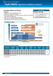
Semiconductor Technologies<br />
R&D Laboratories<br />
Focusing on compound semiconductors which are the key materials for photonic devices<br />
covering ultraviolet to infrared and superior electronic devices indispensable for the<br />
wireless communication, power electronics and optical communication systems, we are<br />
making research and development on the semiconductor materials and their application<br />
technologies, as well as peripheral technologies in these areas.<br />
<strong>Sumitomo</strong> <strong>Electric</strong>’s compound semiconductors and their application<br />
Efficiency (%)<br />
Green semiconductor laser<br />
Innovative plane-direction substrate to overcome the green gap<br />
Green gap<br />
Wavelength (nm)<br />
Electrode<br />
Substrate<br />
Electrode<br />
Green semiconductor laser structure<br />
GaN (0001) plane GaN (2021) plane Green semiconductor laser<br />
Material<br />
Product development and key technologies<br />
CSR approaches<br />
High efficiency<br />
Power devices<br />
OMVPE reactor<br />
Photonic Device<br />
Photonic device<br />
Red laser<br />
Red / Infrared LED<br />
(DVD, PC, automotive and<br />
outdoor display applications)<br />
Infrared laser/<br />
Photo-detector<br />
(Optical communications)<br />
Blue-violet laser<br />
Blue/White LED<br />
(Blu-ray, LCD backlight, outdoor<br />
display and lighting applications)<br />
Ultra-violet laser/<br />
LED<br />
(Sterilization, cleaning and processing)<br />
Electron Device<br />
Construction of Secure and Safe Society,<br />
Preservation of the Environment<br />
Compound<br />
Semiconductors<br />
(GaAs, InP, GaN, AlN)<br />
safer and ecological<br />
manufacturing<br />
processes<br />
OMVPE: Organometallic Vapor Phase Epitaxy<br />
Electronic device<br />
High-frequncy device<br />
Low-noise amplifier<br />
(Mobile phones, wireless<br />
base station and satellite<br />
communication systems)<br />
High-frequency device<br />
High-power device<br />
(Wireless base stations,<br />
power controllers<br />
and electric vehicles)<br />
Next-generation<br />
power device<br />
Core Technologies<br />
Assembly<br />
Design<br />
Device<br />
Process<br />
Characterization<br />
Thin film growth<br />
Equipment<br />
Characterization<br />
High efficiency<br />
Light emitting<br />
devices<br />
Waste gas cleaner<br />
Compound semiconductors are widely used in various<br />
application fields in which silicon devices cannot be used.<br />
<strong>Sumitomo</strong> <strong>Electric</strong> has developed a variety of materials as a<br />
pioneer in this field.<br />
Making use of our technologies of bulk crystal growth,<br />
epitaxial growth, simulation technique, characterization and<br />
analysis, we are making research and development on<br />
high-quality, cost-effective solutions for each applicationspecific<br />
need as well as on the challenge for new materials.<br />
Compound semiconductors are widely used for optical<br />
devices and electronic devices. In each of these areas, we<br />
work on technological development aiming at downstream<br />
products such as epitaxial wafers, devices and modules,<br />
based on our material and device technologies.<br />
Compared with Si semiconductors, GaAs, InP, GaN, AlN<br />
and other compound semiconductors, developed at the<br />
Semiconductor Technologies R&D Laboratories, are environmentally<br />
sound materials contributing to high-voltage<br />
and low-power dissipating operation. We also work on the<br />
development of environmentally friendly process technologies<br />
for the manufacturing processes for these products.<br />
The world’s first pure green semiconductor laser have been successfully developed by taking advantage of <strong>Sumitomo</strong> <strong>Electric</strong>'s<br />
GaN crystal technologies. The development of this green laser realizes red-blue-green (RGB) light sources and leads to<br />
new applications in display market and other fields.<br />
GaN-based transistor<br />
GaN materials have excellent features suited for<br />
electronic device applications. We promote the<br />
development of vertical transistors that make the<br />
most of their excellent features.<br />
The resultant products are expected to surpass Si<br />
devices in speed and energy-saving performance.<br />
Development of Semiconductor Thin Films<br />
Epitaxial<br />
Growth<br />
<strong>Technology</strong><br />
Simulation<br />
<strong>Technology</strong><br />
Unique<br />
Application<br />
<strong>Technology</strong><br />
On-resistance [mΩcm 2 ]<br />
Breakdown voltage [V]<br />
Making use of our technologies of the epitaxial growth, simulation, unique application and the micro-analysis techniques, we<br />
are developing new semiconductor thin films in order to realize innovative devices such as imaging sensors using near infrared<br />
rays and next generation power devices, and so on.<br />
Target<br />
Transmission Electron Microscope (TEM)<br />
Quantum well<br />
structure<br />
InP substrate<br />
Growth technology<br />
of multi-layers<br />
Atomic Force Microscope (AFM)<br />
AlN substrate<br />
Challenge for new materials<br />
in undeveloped-area<br />
Target<br />
Light<br />
sensing<br />
layers<br />
High Al composition<br />
AlGaN thin film<br />
Drain current [mA]<br />
AlGaN/GaN<br />
channel<br />
Vgs=+1V to -3V<br />
step -1V<br />
Source<br />
electrode<br />
Barrier layer<br />
Drift layer<br />
GaN substrate<br />
Drain electrode<br />
Device structure<br />
Near-infrared<br />
ray sensor<br />
Green laser<br />
Power device<br />
Electronic device<br />
Drain voltage [V]<br />
I-V characteristics<br />
Contact layer<br />
Gate electrode<br />
Drain<br />
current<br />
TEM image<br />
35nm<br />
18 19
Information &<br />
Communications Laboratories<br />
Wireless unit for mobile base stations<br />
The Information & Communications Laboratories conduct research and development on information and<br />
communications equipment to create a safe, secure, comfortable and environmentally friendly society.<br />
We work on technological development for optical communications, wireless communications and terminals<br />
that support broadband telecommunications and address the challenges concerning the application<br />
of information and communications technology (ICT) to motor traffic and various other fields.<br />
High-speed optical access system<br />
Speedup via 10G-EPON<br />
10G-EPON<br />
center device<br />
(shared with GE-PON)<br />
IP terminals<br />
Terrestrial/<br />
BS broadcasting<br />
IP set-top box<br />
(IPv6 compatible)<br />
Use of existing PON line<br />
NGN<br />
network<br />
Home gateway<br />
(HGW)<br />
TV<br />
VOD server<br />
IP retransmission<br />
10G-EPON<br />
subscriber’s terminal<br />
10G-EPON<br />
subscriber’s terminal<br />
Phone<br />
IP telephone<br />
network/<br />
server<br />
Subscriber’s<br />
home<br />
Wireless LAN<br />
terminal/mobile<br />
terminal<br />
PC<br />
GE-PON subscriber’s terminal<br />
Shared with<br />
GE-PON<br />
Video service proliferation<br />
Multichannel broadcasting<br />
Higher resolution<br />
Various<br />
servers<br />
Internet<br />
Provide triple-play<br />
services:<br />
phone (IP phone),<br />
video (IP-TV) and<br />
Internet<br />
via safe and high-quality<br />
NGN networks.<br />
We work on the development of small and<br />
Antenna<br />
Internal structure of RRH<br />
Antenna pole<br />
low-power dissipating wireless units (remote<br />
Digital signal<br />
processor<br />
D/A,A/D<br />
converter<br />
to/from<br />
radio head: RRH) for high-speed mobile base<br />
Optical IF<br />
antenna<br />
stations, such as WiMAX and LTE. GaN<br />
Cabinet<br />
devices and envelope tracking(ET) technology<br />
High efficiency amplifier technology have been employed for amplifier efficiency<br />
Envelope Tracking improves amplifier efficiency<br />
Building<br />
improvement. At the same time, our development<br />
roof<br />
Envelope Tracking Fixed bias (non-ET)<br />
Variable bias (ET)<br />
Digital signals<br />
Voltage<br />
efforts are directed toward multi-<br />
antenna technology to support AAS 3 and<br />
Wireless<br />
Time<br />
Base station main unit<br />
signal<br />
Combining all <strong>Sumitomo</strong> <strong>Electric</strong>’s optical component and<br />
MIMO. 4<br />
Configuration of<br />
Reduces power consumed in non-ET mode<br />
system technologies, we work on the technological development<br />
mobile base station<br />
*3 AAS:Adaptive array Antenna System<br />
via optical fiber<br />
of 10G-EPON* 1 to achieve ultra-fast 10 Gbps<br />
*4 MIMO:Multiple Input and Multiple Output<br />
access. Through shared use of the GE-PON* 2 branched<br />
optical fiber network currently in widespread use, 10G-<br />
EPON economically increases the speed of access networks<br />
ICT applied to automobile traffic<br />
10-fold.<br />
Wireless communication system for ITS (UHF band)<br />
Keeps track of accurate traffic conditions by combined the<br />
*1 10G-EPON:10 Gigabit Ethernet Passive Optical Network<br />
- Continuous broadcasting messages (sensor, traffic signal info)<br />
use of sensor information and vehicle probe information.<br />
*2 GE-PON:Gigabit Ethernet Passive Optical Network<br />
- Radio waves are shared for vehicle-to-vehicle<br />
and road-to-vehicle communications.<br />
Traffic signal control<br />
- Traffic signal control To create a society characterized by safe and<br />
for reduced traffic<br />
congestion and<br />
safety transport<br />
energy-saving traffic, we work on the development<br />
of advanced signal control technology<br />
Image sensor<br />
Information from infrastructure<br />
Accurately detects cars and motor cycles.<br />
to prevent collisions<br />
and wireless communications and image<br />
Applied Image System<br />
Onboard network Onboard PLC (in vehicle) sensor technologies incorporated in nextgeneration<br />
Communications data superimposed on power line<br />
Our development efforts include the technological development<br />
Life Science<br />
Power line<br />
PLC modem PLC modem PLC modem<br />
ITS. Our development efforts also<br />
of home gateways (HGW) and IP set-top boxes to pro-<br />
Production<br />
<strong>Technology</strong><br />
Driving Safety Support System<br />
Safety &<br />
concentrate on LAN architecture and onboard<br />
Security Backbone LAN<br />
vide phone, video and Internet services via the nextgeneration<br />
networks (NGN). Efforts are also under way to<br />
Engine Pattern Recognition<br />
<strong>Technology</strong> expansion to various fields<br />
Trunk<br />
Branch<br />
PLC as a future automotive technology.<br />
Image Recognition Image Processing<br />
Branch<br />
&<br />
meet the need for new services in collaboration with mobile<br />
phones and various other information terminals.<br />
ICT applied to safe and secure ubiquitous networking<br />
Application to branch lines<br />
Femtocell<br />
Macro cell<br />
base station<br />
Macro cell<br />
base station<br />
Mobile-phone<br />
operator’s<br />
network<br />
IP network<br />
Femtocell<br />
base station<br />
The femtocell base station has come into focus, which connects<br />
mobile phone handsets at home to mobile-phone<br />
operator’s networks via broadband lines such as FTTH and<br />
ADSL.<br />
We work on the development of a product that, incorporating<br />
<strong>Sumitomo</strong> <strong>Electric</strong>’s proprietary interference mitigation<br />
technology, enables effortless station installation and<br />
achieves a high transmission rate.<br />
Multi-agent technology<br />
Ubiquitous<br />
networking<br />
Product development to make the best use of autonomous,<br />
collaborative and learning agents<br />
Traffic information service system<br />
Travel time<br />
Probe<br />
Travel time<br />
Car Probe<br />
Probe<br />
Optimized<br />
Travel time<br />
Travel time<br />
Multi-agent<br />
system<br />
Services to support humans<br />
Multi-agent system<br />
Travel time<br />
Car<br />
Probe<br />
Travel time<br />
Travel time<br />
Intersection Intersection Probe<br />
Home ICT application technology<br />
Networks<br />
Crime<br />
prevention<br />
Monitoring<br />
Home network<br />
Sensor network<br />
Home<br />
automation<br />
Power consumption<br />
visualization/management<br />
Use of ICT for home safety, security,<br />
amenity and energy conservation<br />
Our development efforts are focused on<br />
multi-agent technology realizing autonomy,<br />
collaboration and learning capability toward a<br />
ubiquitous networking society in which all<br />
kinds of terminals are networked. At home,<br />
various devices and sensors are connected to<br />
a network to provide services or applications<br />
to ensure safety, security, comfort and energy<br />
conservation.<br />
20 21
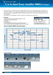
Transmission Devices<br />
R&D Laboratories<br />
Optical Transceivers<br />
At the Transmission Devices R&D Labs, we are developing high performance products widely used<br />
in the communication industries. For optical networks, we have developed high performance optical<br />
devices, optical subassemblies and optical transceivers. We have also developed high speed,<br />
high power electron devices such as HEMTs and MMICs for wireless communication. Our development<br />
is based on vertical integration of creative technologies such as crystal growth of compound<br />
semiconductor, wafer processing, assembling technique, and advanced design ability.<br />
Satellite<br />
communication<br />
Optical<br />
signal<br />
Receiver<br />
Electromagnetic<br />
analysis<br />
Transmitter<br />
IC design<br />
Heat radiation<br />
analysis<br />
RF circuit design<br />
Digital control design<br />
Mechanical design<br />
<strong>Electric</strong>al signal<br />
We are a leading supplier of optical transceivers with small<br />
size and low power consumption, utilizing in-house optical<br />
components/ICs, high-speed analog/digital circuit design<br />
technology, and mechanical implementation technology.<br />
We also contribute toward establishing industrial standards<br />
for optical transceiver specifications, such as<br />
electrical/optical data interfaces and functionality. Our optical<br />
transceiver product family covers a variety of optical<br />
communication interfaces up to 100 Gbit/s.<br />
Rader device<br />
for automotive<br />
Wireless LAN<br />
Wireless Infrastructure<br />
(Long Haul)<br />
Optical communication network<br />
Metro network<br />
Access and PON<br />
Data Center<br />
Wireless<br />
Infrastructure<br />
(Short Haul)<br />
Cellular<br />
Base Station<br />
Wireless Devices<br />
We are a leading company providing GaAs FETs, GaAs HEMTs<br />
(high electron mobility transistors) and GaAs ICs product<br />
family used in a wide range of applications such as satellite<br />
communications and cellular base stations. MMIC (monolithic<br />
microwave integrated circuit) technology is employed in micro<br />
wave and millimeter wave applications.<br />
For next-generation products with higher output power and lower<br />
power consumption, we have successfully developed HEMTs<br />
using the new material gallium nitride (GaN) and have started<br />
mass production of GaN HEMTs for the first time.<br />
Infrared Imaging Sensors<br />
1000<br />
Output power (watt)<br />
100<br />
10<br />
1<br />
0.1<br />
0.01<br />
GaN HEMTs<br />
FET<br />
0.001<br />
1 10 100<br />
Frequency (GHz)<br />
IMFET<br />
PA<br />
LNA<br />
W-CDMA,<br />
PCS,<br />
WiMax,<br />
LTE,<br />
Base Station<br />
HEMT<br />
IMFETs<br />
: Internal matched FET<br />
: Power amplifier<br />
: Low noise amplifier<br />
SATCOM, VSAT, Space,<br />
P-to P Radio<br />
DBS<br />
SATCOM<br />
VSAT<br />
DBS<br />
PA MMICs<br />
PA / LNA MMICs<br />
P-to-P Radio<br />
PA MMICs<br />
Mix / Mult /<br />
Osc MMICs<br />
Rader<br />
: Satellite communication<br />
: Very small aperture terminal<br />
: Direct broadcast satellite<br />
Epitaxial growth technology<br />
InP<br />
Wire<br />
bonding<br />
Wafer<br />
Wafer process<br />
inch<br />
Chip<br />
100 μm<br />
Optical Devices<br />
We have been a leading company of semiconductor optical devices<br />
that are key components in optical communication systems. The product<br />
family covers 10Gbit/s LD, CWDM LD, DWDM electro-absorption<br />
modulators integrated with LDs and tunable LDs, etc.<br />
To provide these devices, we have been developing various edge technologies<br />
such as high quality epitaxial growth technology, sub-micron<br />
wafer process technology, and reliability assurance technology.<br />
Visible<br />
Sensor Chip<br />
Read-Out IC<br />
Near-infarared(NIR)<br />
Automation of Products Quality Inspection<br />
Sensor/Camera<br />
Mid-infrared(MIR)<br />
Mid-infrared camera<br />
Mid-Infrared Laser<br />
Visible Image(CCD)<br />
Near infrared image<br />
Far-Infrared<br />
Toxic・VOC Gas/Environmental Gas Detection System<br />
Si Wafer<br />
We have been developing two-dimensional infrared imaging<br />
sensors based on the photo-detector technologies used for<br />
optical communications.<br />
These sensors have lower noise than conventional ones<br />
and are suitable for microanalysis.<br />
Applications for these sensors can also be found in systems<br />
for two-dimensional diagnosis of tissues, foods and agricultural<br />
products as well as for gas monitoring systems that<br />
measure toxic and environmental gases.<br />
Hermetic<br />
seal<br />
YAG<br />
welding<br />
Optical<br />
Sub-assemblies<br />
10 mm<br />
Optical Sub-Assemblies<br />
Our optical sub-assemblies realize high performance, low power consumption<br />
and compactness with the combination of our own device technologies<br />
such as photo-detectors, light emitting devices, ICs and design<br />
technologies such as high-speed transmission lines and unique packaging.<br />
To meet the requirements of various optical communication systems,<br />
we intend to continuously supply cutting-edge products to the world.<br />
Optical Transceivers for Automotive<br />
Our miniaturized high-speed optical transceiver design technology<br />
with All Grass Fiber (AGF) can be applied to in-vehicle communication<br />
networks as well as public communication networks,<br />
since AGF has a variety of excellent performances, such as wide<br />
bandwidth, small bending loss/radius and high reliability.<br />
W16×D30×H10mm<br />
22 23
Optical Communications<br />
R&D Laboratories<br />
Development of Optical Modules<br />
At the Optical Communications R&D Laboratories, we carry out advanced creative research<br />
and development based on optical fiber technologies, as a foundation for broadband communication<br />
networks. Some of the products we have developed include functional optical<br />
fibers for next-generation optical networks, optical fibers that apply cutting-edge technologies<br />
for popularization of “fiber to the home” (FTTH), and optical interconnections. We are<br />
committed to broadly contributing to society by applying these optical technologies in various<br />
new fields, including for information equipment and optical processing.<br />
Metro<br />
Metro<br />
Amplifier<br />
Long Haul<br />
Metro<br />
Access<br />
(FTTH)<br />
Optical modules developed for use in optical communication<br />
systems contain the following components:<br />
・ROADM (Reconfigurable Optical Add-Drop Multiplexer) for<br />
wavelength switching at optical nodes.<br />
・Er-doped optical fiber amplifier for direct amplification of<br />
optical signals.<br />
・Passive optical components for optical modules (splitter,<br />
wavelength division multiplexer)<br />
Development of Optical Fiber<br />
Splitter<br />
・High spatial resolution monitoring method for passive<br />
optical network (PON) systems using optical coherence<br />
domain reflectometry (OCDR).<br />
Since the early 1970s, the development of Vapor-phase<br />
Axial Deposition (VAD method), an optical fiber manufacturing<br />
technology originally developed in Japan, has been<br />
advanced as a way of mass producing optical fiber.<br />
For functional improvement of optical fiber, renovations in<br />
production technology and structural design are both promoted.<br />
High capacity Fiber for Long Haul Networks<br />
Z-PLUS Fiber enables the launch of a<br />
high power signals, while maintaining low<br />
attenuation characteristics.<br />
Bend-resistant optical fiber for FTTH<br />
PureAccess-R5 has low bending loss,<br />
low loss connectivity with existing fibers<br />
using an original refractive index profile.<br />
Functional Optical Fiber<br />
Fiber Amplifier, Dispersion compensation,<br />
Nonlinear applications.<br />
Pure silica core fiber realizes<br />
world's lowest loss<br />
Z-Fiber boasts the world’s lowest attenuation characteristics<br />
of 0.1484 dB/km @ 1570 nm.<br />
Its optical properties are achieved through the use of a<br />
pure silica core with a fluorine-doped silica cladding.<br />
K. Nagayama et al.,<br />
Electron. Lett., 38 (2002) pp. 1168–1169.<br />
Optical Interconnection Technologies<br />
Multi-fiber optical connectors and connection methods that<br />
consider usability are examined using precise injection<br />
molding technology of submicron accuracy, cultivated as an<br />
optical communication application.<br />
Information equipment requires high-speed transmission<br />
using light for optimal high definition videos.<br />
A ferrule with an integrally molded electrode and optical<br />
fiber hole was developed to simplify the packaging of optoelectronic<br />
devices and optical fibers. This enables great<br />
cost reduction over conventional optical interconnection<br />
modules.<br />
High-Power Optical Applications<br />
Fiber cross section<br />
W. Sakurai et al.,<br />
SEI TECHNICAL REVIEW, No. 66, April 2008, p.134<br />
For optical machining and testing equipment applications,<br />
high-power light sources have been developed.<br />
Pulsed optical fiber laser has high peak optical power of<br />
several tens of kilowatts and high repetition rate over 100<br />
kHz with short pulse duration of few nanoseconds. This<br />
technology has been applied to material processing.<br />
Optical fiber for power delivery such as rectangular formed<br />
optical fiber has been specifically developed. This has<br />
made it possible to form rectangular flat-top beams with<br />
uniform strength distribution.<br />
24 25
Location of research functions<br />
Osaka Works<br />
Newly built main research building<br />
Itami Works<br />
Itami Works, the second oldest works established in <strong>Sumitomo</strong> <strong>Electric</strong>,<br />
were opened in Itami City (Hyogo Prefecture) as the foothold of<br />
products other than electric wires, and had long supported diversification<br />
of the company's business. Presently, the works have the<br />
divisions of special steel wires, hardmetal, powder metal products,<br />
synthetic diamonds, and compound semiconductors, as well as the<br />
R&D division of new materials.<br />
Itami Works<br />
1-1-1, Koyakita, Itami, Hyogo<br />
Tel: +81 72 772 3300 Fax: +81 72 772 2525<br />
Industrial Materials and Process <strong>Technology</strong> R&D Laboratories,<br />
Semiconductor Technologies R&D Laboratories,<br />
R&D General Planning Division<br />
Automotive <strong>Technology</strong> R&D Laboratories,<br />
Electronics & Materials R&D Laboratories, Analysis <strong>Technology</strong> Research Center<br />
Yokohama Works<br />
Among all works of <strong>Sumitomo</strong> <strong>Electric</strong>, Osaka Works have the longest<br />
history and richest tradition. Osaka Works are the foothold of electric<br />
wires and cables (our major products), and info-communications<br />
systems. The works also serve as the foothold of R&D Group and are<br />
creating new businesses one after another.<br />
Osaka Works<br />
1-1-3, Shimaya, Konohana-ku, Osaka 554-0024, Japan<br />
Tel: +81 6 6466 5651 Fax: +81 6 6463 7229<br />
Automotive <strong>Technology</strong> R&D Laboratories,<br />
Electronics & Materials R&D Laboratories,<br />
Analysis <strong>Technology</strong> Research Center,<br />
Power System R&D Laboratories,<br />
Information & Communications Laboratories,<br />
R&D General Planning Division,<br />
New Business Frontier R&D Laboratories<br />
(Water Business /Agriculture Business Development Department)<br />
Industrial Materials and Process <strong>Technology</strong> R&D Laboratories,<br />
Semiconductor Technologies R&D Laboratories,<br />
Transmission Devices R&D Laboratories<br />
Yokohama Works located at southern end of Yokohama City (near<br />
Shonan Area) have largest site area among all <strong>Sumitomo</strong> <strong>Electric</strong><br />
works. The works were opened as the Kanto district foothold of communication<br />
cables. The works presently manufacture various cables<br />
(including power cables and optical fiber cables), optical communication<br />
equipment, and other products. Research and development of<br />
optoelectronics are also conducted here<br />
Yokohama Works<br />
1, Taya-cho, Sakae-ku, Yokohama<br />
Tel: +81 45 853 7182 Fax: +81 45 852 0597<br />
Transmission Devices R&D Laboratories,<br />
Optical Communications R&D Laboratories,<br />
New Business Frontier R&D Laboratories<br />
(Lifescience Business Development Department)<br />
Analysis <strong>Technology</strong> Research Center<br />
Head Office (Tokyo)<br />
Shibaura Renasite Tower 3-9-1 Shibaura,<br />
Minato-ku, Tokyo 108-8539<br />
Tel: +81 3 6722 3100<br />
R&D General Planning Division<br />
The Head Office (Tokyo) is located near JR Tamachi Station, relocated from Motoakasaka,<br />
Minato-ku as of June 2009.<br />
The Head Office is the cornerstone of our Sales Group that deals with various products<br />
and services ranging from national projects and public works to consumer products.<br />
It also acts as a domestic and international hub for information exchange.<br />
Overseas Operations (U.S.A.)<br />
Innovation Core SEI, Inc.<br />
Add : 2355 Zanker Road, San Jose, CA 95131, U.S.A<br />
Tel : +1-408-232-9698<br />
I<br />
C<br />
S<br />
Part<br />
rtic<br />
icip<br />
ipat<br />
ion in<br />
standard<br />
rdiz<br />
atio<br />
n<br />
co<br />
mm<br />
itte<br />
tees<br />
es<br />
Join<br />
int rese<br />
ar<br />
ch<br />
with Ame<br />
merican<br />
un<br />
iv<br />
er<br />
siti<br />
ties<br />
Join<br />
int deve<br />
lo<br />
pm<br />
en<br />
t<br />
with Start<br />
up and<br />
ot<br />
he<br />
r prog<br />
ogra<br />
rams<br />
Info<br />
form<br />
rmat<br />
ion<br />
coll<br />
llecti<br />
tion<br />
/j<br />
oi<br />
nt<br />
de<br />
ve<br />
lopm<br />
pmen<br />
ent<br />
vi<br />
a VC<br />
Busi<br />
sine<br />
ss<br />
opport<br />
rtunit<br />
ity su<br />
rv<br />
ey<br />
for te<br />
ch<br />
nolo<br />
logical<br />
se<br />
eds<br />
IEEE 802.11.15.16, etc.<br />
Support for/implementation of joint research with major universities<br />
Automotive, life science, etc.<br />
Environment, energy and other fields<br />
Smart grid, etc.<br />
S<br />
E<br />
I<br />
26 27