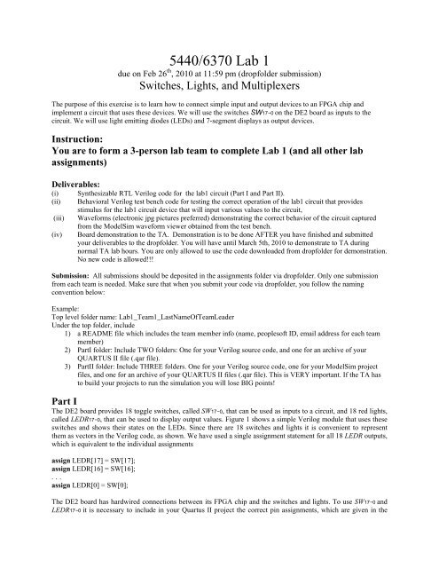
5440/6370 Lab 1
5440/6370 Lab 1
5440/6370 Lab 1

You also want an ePaper? Increase the reach of your titles
YUMPU automatically turns print PDFs into web optimized ePapers that Google loves.
<strong>5440</strong>/<strong>6370</strong> <strong>Lab</strong> 1<br />
due on Feb 26 th , 2010 at 11:59 pm (dropfolder submission)<br />
Switches, Lights, and Multiplexers<br />
The purpose of this exercise is to learn how to connect simple input and output devices to an FPGA chip and<br />
implement a circuit that uses these devices. We will use the switches SW17−0 on the DE2 board as inputs to the<br />
circuit. We will use light emitting diodes (LEDs) and 7-segment displays as output devices.<br />
Instruction:<br />
You are to form a 3-person lab team to complete <strong>Lab</strong> 1 (and all other lab<br />
assignments)<br />
Deliverables:<br />
(i) Synthesizable RTL Verilog code for the lab1 circuit (Part I and Part II).<br />
(ii) Behavioral Verilog test bench code for testing the correct operation of the lab1 circuit that provides<br />
stimulus for the lab1 circuit device that will input various values to the circuit,<br />
(iii) Waveforms (electronic jpg pictures preferred) demonstrating the correct behavior of the circuit captured<br />
from the ModelSim waveform viewer obtained from the test bench.<br />
(iv) Board demonstration to the TA. Demonstration is to be done AFTER you have finished and submitted<br />
your deliverables to the dropfolder. You will have until March 5th, 2010 to demonstrate to TA during<br />
normal TA lab hours. You are only allowed to use the code downloaded from dropfolder for demonstration.<br />
No new code is allowed!!!<br />
Submission: All submissions should be deposited in the assignments folder via dropfolder. Only one submission<br />
from each team is needed. Make sure that when you submit your code via dropfolder, you follow the naming<br />
convention below:<br />
Example:<br />
Top level folder name: <strong>Lab</strong>1_Team1_LastNameOfTeamLeader<br />
Under the top folder, include<br />
1) a README file which includes the team member info (name, peoplesoft ID, email address for each team<br />
member)<br />
2) PartI folder: Include TWO folders: One for your Verilog source code, and one for an archive of your<br />
QUARTUS II file (.qar file).<br />
3) PartII folder: Include THREE folders. One for your Verilog source code, one for your ModelSim project<br />
files, and one for an archive of your QUARTUS II files (.qar file). This is VERY important. If the TA has<br />
to build your projects to run the simulation you will lose BIG points!<br />
Part I<br />
The DE2 board provides 18 toggle switches, called SW17−0, that can be used as inputs to a circuit, and 18 red lights,<br />
called LEDR17−0, that can be used to display output values. Figure 1 shows a simple Verilog module that uses these<br />
switches and shows their states on the LEDs. Since there are 18 switches and lights it is convenient to represent<br />
them as vectors in the Verilog code, as shown. We have used a single assignment statement for all 18 LEDR outputs,<br />
which is equivalent to the individual assignments<br />
assign LEDR[17] = SW[17];<br />
assign LEDR[16] = SW[16];<br />
. . .<br />
assign LEDR[0] = SW[0];<br />
The DE2 board has hardwired connections between its FPGA chip and the switches and lights. To use SW17−0 and<br />
LEDR17−0 it is necessary to include in your Quartus II project the correct pin assignments, which are given in the
DE2 User Manual. For example, the manual specifies that SW0 is connected to the FPGA pin N25 and LEDR0 is<br />
connected to pin AE23.<br />
// Simple module that connects the SW switches to the LEDR lights<br />
module part1 (SW, LEDR);<br />
input [17:0] SW; // toggle switches<br />
output [17:0] LEDR; // red LEDs<br />
assign LEDR = SW;<br />
endmodule<br />
Figure 1. Verilog code that uses the DE2 board switches and lights.<br />
Perform the following steps to implement a circuit corresponding to the code in Figure 1 on the DE2 board.<br />
1. Create a new Quartus II project for your circuit. Select Cyclone II EP2C35F672C6 as the target chip, which is the<br />
FPGA chip on the Altera DE2 board.<br />
2. Create a Verilog module for the code in Figure 1 and include it in your project.<br />
3. Include in your project the required pin assignments for the DE2 board. Compile the project.<br />
4. Download the compiled circuit into the FPGA chip. Test the functionality of the circuit by toggling the switches<br />
and observing the LEDs.<br />
Part II<br />
Figure 2a shows a sum-of-products circuit that implements a 2-to-1 multiplexer with a select input s. If s = 0 the<br />
multiplexer’s output m is equal to the input x, and if s = 1 the output is equal to y. Part b of the figure gives a truth<br />
table for this multiplexer, and part c shows its circuit symbol.<br />
The multiplexer can be described by the following Verilog statement:<br />
assign m = (s & x) | (s & y);
You are to write a Verilog module that includes eight assignment statements like the one shown above to describe<br />
the circuit given in Figure 3a. This circuit has two eight-bit inputs, X and Y , and produces the eight-bit output M. If<br />
s = 0 then M = X, while if s = 1 then M = Y . We refer to this circuit as an eight-bit wide 2-to-1 multiplexer. It has<br />
the circuit symbol shown in Figure 3b, in which X, Y , and M are depicted as eight-bit wires.<br />
Perform the steps shown below.<br />
1, Simulate your design using Silos.<br />
2. Create a new Quartus II project for your circuit.<br />
3. Include your Verilog file for the eight-bit wide 2-to-1 multiplexer in your project. Use switch SW17 on the DE2<br />
board as the s input, switches SW7−0 as the X input and SW15−8 as the Y input. Connect the SW switches to the red<br />
lights LEDR and connect the output M to the green lights LEDG7−0.<br />
4. Include in your project the required pin assignments for the DE2 board. As discussed in Part I, these assignments<br />
ensure that the input ports of your Verilog code will use the pins on the Cyclone II FPGA that are connected to the<br />
SW switches, and the output ports of your Verilog code will use the FPGA pins connected to the LEDR and LEDG<br />
lights.<br />
5. Compile the project.<br />
6. Download the compiled circuit into the FPGA chip. Test the functionality of the eight-bit wide 2-to-1 multiplexer<br />
by toggling the switches and observing the LEDs.