

PDF - DIRAC - CERN
PDF - DIRAC - CERN
PDF - DIRAC - CERN

You also want an ePaper? Increase the reach of your titles
YUMPU automatically turns print PDFs into web optimized ePapers that Google loves.
<strong>DIRAC</strong> Note 2006-01
4P&BDEXHCƒEHY K HC8Ssf‘EcV°KHM.N»Q2K¢Y©CXGg€hBZ0KHSsGJY©€q¦O”“[xo8EcSsiDP^NK¢o8EHfJo8eDfJEcNCdNB©CIWGJYDGJIdeDI<br />
QbEXrpQRCdEHfJQRE<br />
iDGJPNEHYDonCŠ0C8NaQRC8CXYjonKhfJeDIWYDP8£?QGgNB©KheDNSsGJPT?GJY©€dNKWfgK4KhPCFGJY©M*KHSsIqEcNGJKhYœt<br />
QGJYD€dGJYDM,KHSsIWEcNGgKhY®²<br />
_^M,NC8S^NBDGJPbN»Q2K±fJEXrHC8SsPKHM.ÒEcSsiDPbQRC\BDEXHCM,KHSCXEHosBÀÒbEcSsiDPbNB©C\M,KhfJfJK<br />
]&eDI0C8SKHMBGgNP8t<br />
GJYDG‘IeDIÑiDG‘PNEHYDonCŠKHMONaQRK"BDGJNP8t<br />
–<br />
EcSNGJo8efJEcSo8EHPCXP^EcSC\GJPPse©CXi±QB©CXYUNB©C8SsCFEcSCH²<br />
¡<br />
© C8M*NKHS&[Gg€hBZN„×RNB©C\PsfJEcPBDGgNEcSsC\onKhfJfgCXonNCXiœtRAB©C\G‘Y©M,KHS„IqEcNGgKhYUGJPTHC8VN<br />
¦©KHS&CXEHosBj¨&¡`i©C8NCXonNKHSqÖ<br />
GgM‚NB©C8SC\EcSC"ˆ“KHS&†ƒPf‘EcPbM,KHSCXEHosBjEcS„IUtR’&NB©C8SsQGJPCŠEqPV0CXo8GJEHf¤Ec€qGJPPC8NÖ*KHC8S¤DKQ¢KHSCXIqVDNarDׄt<br />
AB©CF[^]^_¤i©CXo8GJPsGgKhY¢QREHP^onKhYDPGJiDC8SCXi¢V0KhPGgNGgHCFGgM2²<br />
QLPGJ€hYDEHfÖ^’Š[É0C8NaQRC8CXYÕNB©Cq¨“¡<br />
AB©C8SCqQbEHPdKhY©CWKHC8S¤DK<br />
†"BDGgNPGJYU¨“¡^[¤KHS&¨&¡ © KHS^IƒKHSCNBDEHY ŽWBDGgNP^GJY ‰ ¦O”ÖÍPeIzKHM<br />
ABDEcN^IƒCXEHYPIƒKHSCNBDEHY<br />
NBDCFßW¦O”“[`ÒbEcS„iDP„ׄt<br />
‰ ¦O”zBDGgNPEHYDiÐKhY©C"¨&¡&[ÑEHYDiÐKhYDC<br />
AB©CW]&]Li©CXo8GJPGgKhYÇGJPŠV0KhPGgNGJHCHt¢AB©CWGJY©Ve©NFGJPq²dNaQRK<br />
© t Ÿ YÐo8EHPC"NB©C8SCWEcSC"IƒKHSCWBDGJNPŠNB©CXYÐEHfJf…NB©CWonKhIGJYDEcNGgKhỸ EcSCqNEcTHCXYÕGJY¥NK EHo8onKheDY¥N<br />
¨“¡<br />
ABDCFi©CXo8GJPGgKhY¢QbEHPonKhYPGJi©C8SCXiUYDC8€hEcNGgHC\GgMR²<br />
Öž’&SKHM‚NB©C ‰ ¦O”¢¨“¡ © EHYDip¨&¡&[&ׄt<br />
AB©C8SCŠQbEHPEHYUCXIƒVNar¤Ec€<br />
©ª© M*Khe©SÒ2›áÒRSsEHiP<br />
”¢&ˆXŽF¦f‘Ec€©tOABDGJPBDEcVDV0CXYDP‚QB©CXYdNB©CIqGJYDG‘IeDI¢iDGJPNEHYonCRM*KheDYDidKhYÈ_<br />
BEHPEqPC8VEcS„EcNGgKhYUKHMˆXŽƒonKhfJeDIWYUEcNfgCXEHPN8t<br />
¡“’Š–¤Ec€©t ‰ GJY©€hfgC“¡^GJN^’“Yp–jefgNGgVfgCFÒ2›áÒbEcS„iDPGJPEHonNGgcEcNCXijGgMEqPGJYD€hfgC&BGgNFÖÍiDGJPNEHYDonCF‡¥×<br />
‰<br />
Ÿ MbGJN\GJP\iDC8NCXonNCXiÕG‘YÀKhYDfgr®KhY©CUÒbo8EcSsiœ£NB©CXYÐNBDC<br />
G‘P\i©C8NCXonNCXi':KJMLN>'OPRQS>TU>á×V7ãßh‡WXht<br />
ˆ ×Y©KWBDGgNPbVSCXPCXYZNGJY¢NB©C\o8EcSsiÇÖ£¢IƒVDN»rU¦f‘Ec€Z×<br />
†h×IƒKHSCFNBDEHY ŽƒBDGgNPFÖž’&HC8S¥¤DK Q¤¦f‘Ec€Z×<br />
‹h×bNB©C\IqGJYGJIqEHf§iDGJPNEHYDonC\§C8N»Q2C8CXY BDGgNPGJPb€HSsCXEcNC8S^NBDEHỸ ˆXŽƒonKhfJeDIqYP8t<br />
ËD̽Ȩ̈¦<br />
¨©<br />
µœ<br />
À¾©ºcºžÂ<br />
© C8M*NF›&¨&¡L[^Gg€hB¥NdEHYDi ‰ ¦”å×<br />
0C8N»Q2C8CXYjNB©CFNaQRK ‰ ¦”`BDGJNPEHYDiUNB©CF¨“¡<br />
© EHYDiU[\t<br />
PsEHIƒC\BDGgNGJPPCXY¥NNaQGJonC\NKqNB©CF]&]¤EHfJ€HKHSsGgNBDIUt<br />
µœ<br />
ÈÂcºžÁ2¸a¾˜¾ hÂ!#"%$§¿œ¸'&Ã(4¼hºžÂ2º)(*<br />
ËDÌ+¦$ÌÍË<br />
ÎÏ#,-/.102,4365<br />
‰ ¦O”LGJPŠSCXEHĩ Khe©NFM*KHS\NB©CqKHØ"GJY©CqQGJNBÀEjA”FÒxPsGg€hYDEHfOQBDG‘fgCÈM,KHSNB©CWNSsGJ€H€HC8S\NB©C ‰ ¦”LG‘P<br />
AB©C<br />
PsGg€hYDEHf^ÖÍAIqAªS„Gg€hAªKh_&”FÒׄt Ÿ YÇ_SsG‘EHY©CH£EcM*NC8SÈNB©C±†c‡H‡©ˆ¢iDEcNE NEcT?GJY©€jNBDC<br />
PNEcSNCXiÕ4rÀNB©C"_&”FÒ<br />
onKhfJeDIWYDP8£heDN.NB©C^PNEcSsNGJY©€FV0KhGJYZN<br />
KHMRNBDGJP&ßh‡HYDPFGJP“NeY©CXi°Zr®BDEHYDi®EHYDiÀY©KQB©C8SCƒQSsGgNNCXYœ£$EHYDiÀonKhefJi°(EcSr®GJYDPsGJi©CEHYÀG‘Y¥NC8ScEHfOKHM<br />
c‡HYDP8t.AB4eDP.NBGJP.onKheDfJiqG‘Y¥NSK?iDeDonCEFiGÔm§C8SsCXY¥N…Y4eDI§C8S.KHMœBDGJNP.PC8CXYq4rNBDCNSsGg€H€HC8SEHP2onKhIƒVEcSCXi<br />
†
¢¡pÚ$Τ£¦¥¨§A,© .<br />
ËDÌ+¦$ÌJÙ<br />
KHMFNB©C°NSsGg€H€HC8SUEHYDiEHfJf^NB©C°V0KhPPGgfJCjo8EHPCXPUEcSCÀPNKHSCXiGJYÝNB©CÀ–jEHPNC8Spo8EcSsiDP8£YDK<br />
AB©C®fgKH€hGJo<br />
<br />
¤Ec€qM*KHS^GgNQbEHPGJY¢NBDC<br />
NBDC\[]&_¤NSsGg€H€HC8SQbEHPY©KHN^GJYUNB©CFi©CXo8G‘PGgKhYUKHMNB©CFNSsGJ€H€HC8Se©NNBDC<br />
BEcSsi©QbEcSCÖÍA‡¥ç“Aß\iDEcNE\G‘Yq†c‡H‡h‹hׄt2AB©CXYqKhYqNBDGJPiDEcNEŠNB©C&[]&_ÝNS„Gg€H€HC8S2PG‘IeDf‘EcNGgKhYÈQREHP<br />
NSCXEHIUtÉAEcfgC ˆ®PB©KQP¢NB©C®SCXPeDfJN"QGJNB NB©C®HC8SNCn¬¤¦OGgNUonKhYDiDGgNGJKhYDP8t AB©C®[]&_ G‘P<br />
‰<br />
PG‘IeDf‘EcNGgKhY<br />
EcVVEcSCXYZNfgr°fJCXPPŠQRCXfJf.PGJIdeDfJEcNCXi®NBDEHYÇ”“]^_tªAB©CqIWEHGJYÀo8EHeDPCqKHMbNB©C"[]&_<br />
KHM*NaQbEcSC*)шF¡&EcSsi©QbEcSC*)x‡ ‰ KHM,N»QREcSsC*)`‡q¡&EcSsi©QbEcSC*)ш<br />
‰<br />
Ž4t ,+ ÖʈX‹H†?ˆXŽh× †4t—ß-+ Ö½ŽHŽH´Hh×<br />
”“]&_¤EHfJKhY©C<br />
BDGgNP“PC8CXY®4rjNBDC<br />
MÍEHGJfJeDSC¢ÖÍG‘YÕˆX´H†H´?ˆqC8HCXY¥NPŠKheDNŠKHMR‹c‡h†HŒH´hדGJPŠie©CNKpo8EHPCXPŠKHMNK4KpIqEHYZr<br />
EHYDiãYDKHNƒZrÕNB©CjBDEcS„i©QREcSsCUNSsGg€H€HC8SXt Ÿ Y NBDG‘PÈVEcSNGJo8eDf‘EcSqo8EHPCpNB©CjPKHM,N»QREcSC<br />
PsGJIefJEcNGgKhY<br />
QRKheDfJiW€hGgHC“E\V0KhPGgNGJHCi©CXo8GJPGJKhYqQBDG‘fgCM*KHS2NB©C&BDEcSsi©QbEcSC&GgN2GJP2Y©C8€hEcNGgHCHtAB©C^o8EHeDPC&onKheDf‘i<br />
‰ ¦O”d£<br />
0C\IdeDfgNGJVfgCH£©EHYpC8SSsKHSGJYUNB©CosB©KhGJonCKHMONB©CF€hEcNCdM,KHS^NB©C\EH¯4eDGJPGgNGJKhY¢KHMNBDC\BDGgNPG‘Y<br />
’“[¢”&]&_ ¨.C8SsNCn¬¢NS„EHoT?GJY©€ ”&K QY ‰ NSCXEHINSsEHoT?GJY©€<br />
[^]^_<br />
´H‹4t—ß=+ ´H‹4t—ß=+<br />
EHfJf5476$EHYDijEHfJf84:9ƒEHYDi;47<<br />
J1AUEHYDi(BDC XZÖE479h× 7 ˆ8‡? JFA ´H´4tG.H+ ´H´4t ,+<br />
4>67ã†H†@?<br />
J1AUEHYDi(BDC XZÖE479h× 7 ßI? JFA±EHYi(BJC X4ÖE4:67¤ˆXŽ@?<br />
i©K?o8eDIƒCXYZNPEcSC\E (EHG‘fJEcfgCŠKhYpBDK Q NKqSsCXEHijGgNEc€hEHGJY$£DEHYDipB©KQ Cn¬?EHonNfJr¢GJNQREHPM*eDYonNGgKhYDGJY©€©t<br />
ËDÌ+¦$̧¦ Τ/5§ . 5<br />
‰ t4¨“fJEHosB©KhPFÖ*VSsGgcEcNC“onKhIWIeDYGÔ›<br />
’“Y©C&HC8SsPGJKhY¢KHMªNB©C“]CXeDSsEHfœ]C8N»Q2KHSsT±onK?i©CŠBDEHPR0C8CXY"M*KheDYDi±4r<br />
o8EcNGgKhYדe©NŠB©CƒonKheDfJiÀY©KHNŠSsCXIƒCXI\0C8SŠQRC8NB©C8SFNBDG‘P“QREHPŠNBDCƒKhY©CqeDPCXi®M*KHSFNB©CƒNSsEHG‘YDGJY©€±KHM2NBDC<br />
EHonNeDEHfªNSsGg€H€HC8SGJYp†c‡H‡©ĉt<br />
|$}! ¤}{#"%$&R{<br />
”&EcNE"PCXfgCXonNGgKhY$t<br />
YqKHS„i©C8SNKC8(EHfJeEcNCNB©C&[]&_¤PGJIdeDfJEcNGgKhYÈKHMœNB©CNSsGg€H€HC8SX£4SCXEHfiEcNEFQRC8SC^PCXfJCXonNCXiWQBDCXY<br />
Ÿ<br />
EcVVfJGgCXiœt&AB©CdPGJIdeDfJEcNGgKhYjNEcTHCXPFEHP“GJY©Ve©NNB©CKHØ"GJY©C\cEHfJe©CXP&KHM…NBDCcEcSsGJEcfJCXP8£§PsGJYDonC\NBDC<br />
SsCXEHfœBDEcSsi©QbEcSC“GJY©Ve©NRGJPbY©KHNPNKHSCXiUGJY±NB©CŠiDEcNE?t2AB©C“BDEcSsi©QbEcSCŠi©CXo8GJPGJKhYWQbEHPonKhIƒVEcSCXi<br />
Q^GgNBFNB©C2PGJIdeDfJEcNGgKhYFiDCXo8GJPGgKhYFEHYiFNB©CRYZeDI0C8S$KHMDonKhGJYDo8G‘i©CXYDonConKheDYZNCXiœtOAB©C…C8HCXYZNPOBDEXHC<br />
‰ NSsCXEHIEHYDi('^V ‰ NSsCXEHI<br />
NK"PEcNGJPM*r"NBDCŠ¨.C8SNCn¬p¦GJNAªSsEHosT4G‘Y©€WonKhYDiDGJNGgKhYDPbeDPGJYD€dNBDCF”^KQY<br />
iDC8NCXonNKHSsP8t<br />
ÒbKhIƒVEcSsGJPKhY¢KHMOBEcSsi©QbEcSC“›PKHM*NaQbEcSC\M*KHS[]&_t<br />
’“M2E¢NKHNEHf…KHMŒ(ßh‡©ˆX´HŒUC8HCXYZNP8£.†H‹HŽc‡hŽHÚC8HCXYZNPFQRC8SCƒSCXonKhYDPNSseDonNCXiÀQGJNB®NB©CȨ.C8SNCn¬Ð¦GJN<br />
[^]^_`EHfgKhY©C ˆX†4t ´-+ Ö½‹c‡h†HŒH´h× .Zt ‹-+ Öʈ/.c†HŒH´h×<br />
AEcfgCqĉ² Ÿ Y©C10"o8GgCXYDonr±KHMNBDCF”&]&_`EHYDip[^]^_¤NSsGg€H€HC8S^PGJIdeDfJEcNGgKhYDPXt<br />
PKhIƒC8NBDGJY©€dIqGJPPsGJY©€\GJYWNB©CŠ–pKHNB©C8SÒbEcS„iœ£¥KHS32eDPN2EiDGÔm0C8SCXYZN2fJGJIWGgNGJYWNB©C^KHC8S¤DKQ<br />
¦f‘Ec€©£<br />
GJCHtIƒKHSCFBDGJNPbQ2C8SCEHfJfgK QRCXipGJYpNB©CFBDEcSsi©QbEcSCHt<br />
ÒbKhIƒVEcSsGJPKhY¢KHMOBEcSsi©QbEcSC“›PKHM*NaQbEcSC\M*KHS”“]^_¤KHS&[]&_<br />
ABDGJY©€hP.EcSC€HKhGJY©€FIdeDosBW§C8NNC8SM,KHS…NBDC&’“[ãKHM0NB©CPsGJIefJEcNGgKhYDPOM*KHS”“]^_EHYDiW[]&_\£hNBEcN<br />
QbEHPEHonNeEHfJfgr¢eDPCXipGJY¢NBDCŠSseDYDYDG‘Y©€©t<br />
AEcfgC\†4² ¢K0Wo8GJCXYDonrWKHMONB©C\”“]&_<br />
’“[«[^]^_¢NSsGg€H€HC8S&PGJIdeDfJEcNGgKhYDPXt<br />
‹
Q^Y ‰ NSCXEHINSsEHoT?GJY©€qQRC8SC\onKhIqVEcSCXiœ£PC8C<br />
¦DKHS^NBDG‘PbNCXPNNB©CF¨.C8SsNCn¬pNSsEHoT?GJY©€WEHYiUNB©C\”&K<br />
AEcfgC\†4t2AB©CŠSCXPefgNEcSCŠHC8SrUPGJIWGJfJEcSXt<br />
¢¡¾4¼jÂ!&ÅÀÆÇ· cº$ãøa¿¼hºa ¤¼hľ¤£¦¥¨§¿¼H¿O<br />
Oaµ<br />
KHMÍEcSX£hGJYNB©CEHYDEHfgr?PGJPKHMNBDC†c‡H‡©ˆiEcNE“KhYDfgrF”“]^_ÝQbEHP.PGJIdeDfJEcNCXiÈGJYNB©C–pKhYZNCÒbEcSsfgKhPXtO”&KhGJYD€<br />
‰<br />
çzAß°ç ÖÍ[]&_ KHSÈ”“]^_Š×“QRCqKHDNEHG‘YÐàD€he©SsC"†4tÀC<br />
0C8CXYÐEcVDVf‘GgCXi®QGgNBÀNBDCWMÍeDfJfNSsGg€H€HC8SX²ÈA‡<br />
GJY¥NSsK4iDeonC¢Ẽ PfJGg€hBZN,4@4>6i©C8V0CXYDiDEHYonCUKHM&fgCXPsPƒNBDEHY ‡?tJˆ/+ M,KHS<br />
onKhYDo8fJei©CUNBDEcNW”“]&_\t—KHSXtl[^]^_<br />
ĉ²ãÒRKheDfJeI\ ÒRKHSSCXf‘EcNCXi –pKhYZNCÒbEcSsfgK C8HCXYZNP8tÑ[EcNGgK KHMC8HCXY¥NP PCXfgCXonNCXiQGJNBÝNBDC<br />
¦OGg€he©SC<br />
4>6$EHYDi;4ƒt<br />
A‡¥ç“AßZçƒÖÍ”“]^_¤KHS[^]^_Š×³ÈA‡¥çŠAßZç“”“]^_`EHPM*eDYonNGgKhY¢KHM<br />
ÒRKHSSCXf‘EcNCXi –pKhYZNCÒbEcSsfgK C8HCXYZNP8tÑ[EcNGgK KHMC8HCXY¥NP PCXfgCXonNCXiQGJNBÝNBDC<br />
¦OGg€he©SCІ4²ãÒRKheDfJeI\<br />
4>6$EHYDi;4ƒt<br />
A‡¥ç“AßZçƒÖÍ”“]^_¤KHS[^]^_Š×³ÈA‡¥çŠAßqEHPMÍeDYDonNGgKhY¢KHM<br />
NBDGJPQ2C\BEXHCfJKhPNPKhIƒCFC8HCXYZNP&EHYDiUNB©C8rUPB©KQ¢E,4>6$i©C8V0CXYDi©CXYonCH£DPGJIqGJf‘EcSRM*KHS:4ƒ£DKHM.fgCXPPbNBDEHY<br />
‹+æM*KHS4È£© 4>6© ˆXŽƒ–jC8¨£©àD€heDSCdĉt2ABDGJPRiDGÔm0C8SCXYDonCŠfgCXEHiDPRNKqEȇ?t Ž+ÑIƒKHSsCFÒÒ2›žEHoT4€HSKheDYi<br />
‡?t<br />
NBDEHYUQ^GgNBU”“]^_`PGJIdeDfJEcNGJKhYUEHfgKhY©CHt<br />
M.Q2CÈonKhIƒVEcSsCNB©Cƒ–®Ò¤C8HCXYZNP“QB©C8SCNB©C\NS„Gg€H€HC8SŠPGJIdeDfJEcNGgKhYDPKHMA‡WEHYi AߢEHfgKhY©CdBDEXHC<br />
Ÿ<br />
4È£© 4>6©<br />
ˆXŽW–pC8¨dt<br />
ß
_^M*NC8S.Khe©Sf‘EHPNIqC8C8NGJY©€“NB©CbosB©CXosTKHMiEcNE(›žNEcT4GJYD€&V0C8SsGJK4iDP‚GJYȆc‡H‡©ˆbQGgNBdiDGÔm0C8SCXY¥N‚NSsGg€H€HC8SsP<br />
QbEHPV0C8SM*KHSsIƒCXiœt.A‚KƒàYDi±Khe©NEHonNGgHC\NSsGg€H€HC8SsPonKhYZNCXY¥N^KHM‚NS„Gg€H€HC8SA”FÒ‹H‹.@.dQbEHPosBDCXoTHCXi<br />
NS„Gg€H€HC8S^GgNPCXfgM ¥<br />
NS„Gg€H€HC8S§¦‘Ö*C8C©¨ © EHI\œiDE¨ÓFEcKhY¨§”“]&_dÖž’“[“ר§”“]^_dˆ¨§”“]&_&†h× )ÕNS„Gg€H€HC8S¦l‡(¬Dc‡cßhEcß<br />
¥<br />
A\ˆnVGgVGJonKHVf
<strong>DIRAC</strong> RNA-Trigger<br />
Hardware Overview<br />
Revision 1.3<br />
Physics Basel, 14. December 2000, M. Steinacher<br />
1. Introduction:<br />
This paper gives an overview of the hardware needed for the Revised Neural Atomic trigger<br />
(RNA-trigger) at the <strong>DIRAC</strong> experiment (<strong>CERN</strong> / PS212). This trigger works similar to the already<br />
installed <strong>DIRAC</strong> Neural Atomic trigger (DNA-trigger); instead of the 16 channel Ionizing<br />
Hodoscope the 240 channel Vertical Scintillating Fibers (SciFi[1..240]) are used to locate the pionpair<br />
in front of the Spectrometer Magnet. After the Spectrometer Magnet the hit-maps of the two 18<br />
channels Vertical Hodoscopes Left (VL[1..8]) and Right (VR[1..18]) are used to track the two pions.<br />
The analog detector signals are digitized with discriminators and preprocessed by the Preformat &<br />
Decision Electronics (PDE) before the appropriate NN-patterns are transferred to the four<br />
NN-CARDs (built for the CP-LEAR experiment / <strong>CERN</strong> / PS195). The four NN-decisions are wired<br />
to the PDE where the final RNA-decision is made. To reach a RNA-decision time of only several<br />
hundred nanoseconds, the whole PDE must be realized with fast digital electronics. The PDE as<br />
well as the NN-CARDs are located in the RNA-CRATE and they are loaded and controlled via the<br />
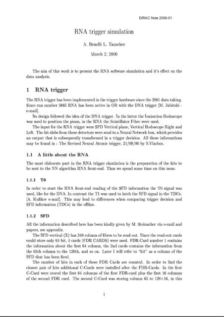
J1-VMEbus. Figure 1 shows the origin of the <strong>DIRAC</strong> detector-signals used for the RNA trigger.<br />
p<br />
A golden pionic atom event in the <strong>DIRAC</strong> detector<br />
Target<br />
+<br />
_<br />
1<br />
240<br />
Vert. Scintillating Fibers<br />
SciFi (240)<br />
disc.<br />
Spectrometer<br />
Magnet<br />
VR(18)<br />
VL(18)<br />
2<br />
1<br />
2 1<br />
disc.<br />
Vertical Hodoscopes<br />
17<br />
18<br />
18<br />
17<br />
disc.<br />
+<br />
_<br />
For an introduction to the RNA-trigger see<br />
the paper 'The Revised Neural Atomic trigger',<br />
S.Vlachos, Basel, 21. September 2000.<br />
The already installed DNA-trigger is<br />
documented in the following papers:<br />
• 'The Dirac Neural Atomic trigger',<br />
S. Vlachos, Basel, 18. November 1998.<br />
• 'Interface & Decision CARD', M. Steinacher,<br />
Basel, 9. August 1999.<br />
• 'The neural network first-level trigger for the<br />
<strong>DIRAC</strong> experiment', P. Kokkas et al., will be<br />
published in Nucl. Instr. and Meth. A<br />
SciFi[1..240]<br />
VR[1..18]<br />
VL[1..18]<br />
to RNA-trigger<br />
Figure 1<br />
<strong>DIRAC</strong> detectors used for the RNA trigger: The analog signals from the Scintillating Fibers<br />
(SciFi[1..240]) and the Vertical Hodoscopes Left and Right (VL[1..18], VR[1..18]) are<br />
discriminated and the digital signals are connected to the RNA-trigger.<br />
<strong>DIRAC</strong> RNA-Trigger Hardware Overview Version 1.3 1 of 10
2. Layout:<br />
The RNA-trigger hardware can be subdivided into two main parts: The Preformat & Decision<br />
Electronics (PDE) and the Neural Network (NN). The description of the NN-electronics is not part<br />
of this article; it can be found in the following papers: 1 ) 'NN-CARD DESIGN', M. Steinacher,<br />
Basel, 11. September 1992. 2) 'NN-CARD PROTOTYPE', M. Steinacher, Basel, 27. September<br />
1993.<br />
The PDE converts each of the three detector hit-maps [SciFi(240), VL(18), VR(18)] into two<br />
binary numbers, representing the position of the hits. The two positions extracted from the 240<br />
channel SciFi are coded in two 8 bit numbers [SciFi_POS1/2(16)] representing the two closest hits.<br />
The two positions of the 18 channel VL are coded in two 5 bit numbers [VL_POS1(5), VL_POS2(5)]<br />
and the same scheme is also used for VR [VR_POS1(5), VR_POS2(5)]. These six binary number are<br />
combined to build the four different NN-patterns. Each of the NN-patterns holds the two SciFi<br />
positions and a combination of one VL-and one VR-positions. This results in four different 26 bit<br />
wide NN-patterns. All NN-CARDs are loaded with the same weights, optimized to distinguish from<br />
a good and bad event. Further the PDE forms the final RNA-decision (RNA_DEC), manages the<br />
correct internal timing of the RNA-trigger sequence (SciFi_GATE, NN_CLK, V_CLK) and the<br />
communication with the '<strong>DIRAC</strong> Trigger Control' via the following signals: T0_START, BUSY,<br />
VETO, RNA-DEC and STRB.<br />
<strong>DIRAC</strong><br />
Trigger<br />
Control<br />
Preformat & Decision Electronics (PDE)<br />
T0_START<br />
BUSY<br />
VETO<br />
RNA_DEC<br />
STRB<br />
Neural Network (NN)<br />
SciFi_POS1/2(16)<br />
SciFi[1..64]<br />
FDR-CARD<br />
#1<br />
C-CARD<br />
#1<br />
SEL1<br />
HITS1(4)<br />
MIN_DIST1(4)<br />
VL_POS1(5)<br />
NN_DEC1<br />
VR_POS1(5)<br />
NN-CARD<br />
#1<br />
SciFi(240)<br />
SciFi[65..128]<br />
SciFi[129...192]<br />
SciFi[193..240]<br />
FDR-CARD<br />
#2<br />
FDR-CARD<br />
#3<br />
FDR-CARD<br />
#4<br />
16<br />
C-CARD<br />
#2<br />
16<br />
C-CARD<br />
#3<br />
16<br />
C-CARD<br />
#4<br />
SEL2<br />
HITS2(4)<br />
MIN_DIST2(4)<br />
SEL3<br />
HITS3(4)<br />
MIN_DIST3(4)<br />
SEL4<br />
HITS4(4)<br />
MIN_DIST4(4)<br />
M-CARD<br />
NN_DEC2<br />
NN_DEC3<br />
VL_POS2(5)<br />
NN_DEC4<br />
VR_POS2(5)<br />
NN-CARD<br />
#2<br />
NN-CARD<br />
#3<br />
NN-CARD<br />
#4<br />
SciFi_GATE<br />
NN_CLK<br />
VL(18)<br />
VR(18)<br />
Figure 2<br />
The Layout of the RNA hardware: The main block is the PDE part, which converts the<br />
detector hit-maps into four different NN-patterns. It also manages the correct internal timing<br />
as well as the communication with the '<strong>DIRAC</strong> Trigger Control'. The NN is trained to be<br />
selective between good and bad events.<br />
<strong>DIRAC</strong> RNA-Trigger Hardware Overview Version 1.3 2 of 10
The PDE itself consists of total nine VME-cards (4 FDR-CARDs, 4 C-CARDs, 1 M-CARD)<br />
from three different types with the following functionality:<br />
2.1 Fanout / Delay / Register Card (FDR-CARD):<br />
The name Fanout / Delay / Register Card already implies its functionality: First the FDR-<br />
CARD receives/fanout the SciFi-signals arriving in differential ECL (dECL) level on the<br />
frontpanel. Since the SciFi-signals are not only used for the RNA-trigger, the fanout is<br />
necessary.<br />
Then the received SciFi-signals are delayed by an adjustable amount of time (around<br />
150..200ns). This is inevitable because the SciFi-signals are valid prior the lowest level trigger<br />
(T0_START) of the <strong>DIRAC</strong> experiment. The adjustable delay step-size can be around 5..10ns<br />
because the SciFi_GATE, coming from the M-CARD, can be adjusted with a resolution of 0.5ns<br />
(via the VMEbus) with respect to T0_START.<br />
Finally the FDR-CARD registers the delayed SciFi-signals during the SciFi_GATE (dECL)<br />
is active. This is needed due to the fact that the SciFi-signals arrive in a time-window of about<br />
40ns. The SciFi_GATE signal is generated on the M-CARD and it is connected to the FDR-<br />
CARDs via the frontpanel. Since the same SciFi_GATE signal is used on all of the four FDR-<br />
CARDs, it is necessary that the 110Ω termination resistors can be removed; the SciFi_GATE<br />
signal is daisy-chained from FDR-CARD #4..#1 and it is terminated on the last FDR-CARD #1.<br />
The entire 240 SciFi-signals are covered by four identical FDR-CARDs. One FDR-CARD<br />
is able to handle 64 SciFi inputs connected via the frontpanel. Since the FDR-CARD #4 uses<br />
only 48 inputs out of the 64 inputs, the SciFi inputs which are left open should be defined low.<br />
The TTL level outputs of the FDR-CARDs are connected via the J2-connector (96 pin,<br />
DIN41612) to the dedicated RNA-backplane where they are distributed to the C-CARDs. The<br />
outputs of the FDR-CARDs are able to drive termination on the C-CARDs of 180Ω to +5V and<br />
330Ω to GND. Since the first 16 SciFi-signals are wired to two different C-CARDs these<br />
outputs are duplicated and buffered separately. Therefore 80 pins out of the 96 pins on the J2-<br />
connector are used; the remainder are connected to GND.<br />
<strong>DIRAC</strong> RNA-Trigger Hardware Overview Version 1.3 3 of 10
2.3 Concentrator Card (C-CARD):<br />
Each Concentrator Card (C-CARD) processes in parallel 80 registered TTL SciFi-signals<br />
from two adjacent FDR-CARDs. To get a continuos and constant detection performance over<br />
the whole width of all 240 SciFi channels, an overlap of 16 channels between two adjacent<br />
C-CARDs is implemented. The C-CARD #1 processes the 64 registered TTL SciFi-signals from<br />
the FDR-CARD #1 and the lowest 16 registered TTL SciFi-signals from FDR-CARD #2. The<br />
same scheme is also used for the C-CARD #2 and #3; the C-CARD #4 treats only the 48<br />
registered TTL SciFi-signals from FDR-CARD #4. Nevertheless all C-CARDs are completely<br />
identical.<br />
The three main tasks of the C-CARD are:<br />
• Find in the 80 bit hit-map the two hits which has the smallest distance (closest<br />
together). Send the detected minimum distance [MIN_DIST(4)] via dECL signals on<br />
the frontpanel to the M-CARD. If a single hit is detected set the minimum distance to<br />
zero. Two adjacent hits correspond to a minimum distance of one. Up to a distance of<br />
14 the algorithm is linear. The minimum distance of 15 indicates that the distance is<br />
equal or bigger than 15 or no hit is detected in the 80 bit hit-map.<br />
• Count the number of hits in the lower 64 bit of the hit-map; this restriction makes sure<br />
that each hit is counted only once. Send the number of hits [HITS(4)] via dECL signals<br />
on the frontpanel to the M-CARD. If more than 15 hits are counted, it saturates at 15.<br />
• If the C-CARD is selected, the two absolute positions (each 8 bit) of the two closest<br />
hits are presented on the tri-state bus [SciFi-POS1/2(16)]. If there was only a single hit,<br />
two times the same position is presented. The absolute positions of the hits are<br />
calculate by using the VME address of the selected C-CARD. The select signals<br />
[SEL1..4, dECL] are generated on the M-CARD and they are connected to the C-<br />
CARDs via the frontpanels. The outputs of the C-CARD are able to drive terminations<br />
on the NN-CARDs of 180Ω to +5V and 330Ω to GND.<br />
The distribution of the registered TTL SciFi-signals from the FDR-CARDs to the<br />
C-CARDs and the interconnection of the tri-state TTL bus [SciFi-POS1/2(16)] to the NN-<br />
CARDs are realized on the RNA-backplane. All the 96 pins of the J2-connector are used for the<br />
signal interconnection [input: TTL SciFi-signals(80), output: SciFi-POS1/2(16)].<br />
<strong>DIRAC</strong> RNA-Trigger Hardware Overview Version 1.3 4 of 10
2.3 Master Card (M-CARD):<br />
The Master Card (M-CARD) receives and processes the information from the four<br />
C-CARDs. All the signals from the C-CARDs are transmitted to the M-CARD in dECL format<br />
and are connected via the frontpanel. The M-CARD selects the C-CARD which has sent the<br />
smallest minimum distance [MIN_DIST1..4(4)]. This selection is accomplished by the outputs<br />
SEL1..4 (dECL) on the frontpanel of the M-CARD. If two or more C-CARDs send the same<br />
minimum distance the first C-CARD in the order #1, #2, #3, #4 is selected. Out of the four<br />
number of hits [HITS1..4(4)] the Total Number of Hits (TNH) in the SciFi detector can be<br />
calculated. If TNH is zero (no hit) the SciFi_EMPTY is activated; if TNH is bigger than 5 the<br />
SciFi_OVR is activated. A smallest minimum distance of 15 and the SciFi_EMPTY not<br />
activated, indicates one or more hit-pairs with a Distance Equal or Bigger than 15 (DEB15).<br />
By combining the four minimum distances [MIN_DIST1..4(4)] and the four number of hits<br />
[HITS1..4(4)], Single Hits 0n Multiple (SHOM) C-CARDs can be detected. The four facts<br />
SciFi_EMPTY, SciFi_OVR, DEB15 and SHOM are needed for the final RNA-decision.<br />
The M-CARD processes also the two detector hit-maps VL(18) and VR(18). The dECL<br />
signals are connected to the M-CARD via the frontpanel; the 110Ω termination resistors can be<br />
removed and the signals can be daisy-chained to the already installed DNA-trigger. The M-<br />
CARD registers the VL and VR hit-maps on the rising edge of the V_CLK signal which is<br />
adjustable with a resolution of 0.5ns (via VMEbus) with respect to T0_START. For each side of<br />
the Vertical Hodoscope, up to two hits can be processed. The M-CARD determines, separately<br />
for VL and VR, the position of the hit(s) and they are coded in four 5 bit values [VL_POS1(5),<br />
VL_POS2(5), VR_POS1(5), VR_POS2(5)]. If only one hit is registered two times the same<br />
position is readout. Further the VL_EMPTY, VR_EMPTY (no hit) and VL_OVR, VR_OVR (more<br />
than 2 hits) are build to perform the final RNA-decision. The four positions of the Vertical<br />
Hodoscope are distributed to the NN-CARDs via the J2-connector and the RNA-backplane.<br />
Because each of the position is used on two different NN-CARDs they are duplicated and<br />
buffered separately. The outputs are able to drive terminations on the NN-CARDs of 180Ω to<br />
+5V and 330Ω to GND. The NN_CLK signals [NN_CLK1..4] are buffered for each NN-CARD<br />
separately and are able to drive terminations of 82Ω to +5V and 120Ω to GND. Therefore 44<br />
pins out of the 96 pins on the J2-connector are used; the remainder are connected to GND.<br />
The signal T0_START (dECL) is connected via the frontpanel and starts the programmable<br />
sequencer which steers the timing of the RNA-trigger sequence. An active VETO input signal<br />
(dECL) prevents the RNA-trigger from processing new events. The timing of the RNA-trigger is<br />
controlled by the signals Sci_Fi_GATE, V_CLK, NN_CLK and STRB. During the RNA-trigger<br />
is running the signal BUSY (dECL) on the frontpanel of the M-CARD is activated.<br />
The four NN-decisions [NN_DEC1..4, dECL] are connected to the M-CARD via the<br />
frontpanel. The final RNA-decision is a dECL signal available on the frontpanel of the M-<br />
CARD and a 20ns STRB signal (dECL) indicates that the RNA-decision is valid. The final RNAdecision<br />
is carried out on the M-CARD using the following algorithm:<br />
EMPTY<br />
SPREAD<br />
OVR<br />
NN_OR<br />
= SciFi_EMPTY or VL_EMPTY or VR_EMPTY<br />
= DEB15 or SHOM<br />
= SciFi_OVR or VL_OVR or VR_OVR<br />
= NN_DEC1 or NN_DEC2 or NN_DEC3 or NN_DEC4<br />
RNA_DEC = OVR or (NN_OR and not EMPTY and not SPREAD)<br />
<strong>DIRAC</strong> RNA-Trigger Hardware Overview Version 1.3 5 of 10
3. Signal Interconnections:<br />
Figure 3 shows the signal interconnection diagram of the RNA-trigger. The most connections<br />
between the 13 cards are realized on the dedicated RNA-backplane with single ended TTL signals.<br />
The dECL detector signals are connected via the frontpanels of the FDR-CARDs and M-CARD. For<br />
daisy-chain purpose all dECL 110Ω termination resistors can be removed.<br />
NN_CLK4<br />
VR_POS2(5)<br />
SciFi_POS1/2(16)<br />
NN-CARD #4<br />
VL_POS2(5)<br />
VMEbus (J1)<br />
Tri-State BUS<br />
BACK: Interconnections on dedicated RNA−Backplane via J2 (all signals single ended TTL)<br />
NN_CLK[1..4]<br />
VL_POS1(5)<br />
VL_POS2(5)<br />
VR_POS1(5)<br />
VR_POS2(5)<br />
VL_POS1(5)<br />
VR_POS1(5)<br />
SciFi_POS1/2(16)<br />
NN_CLK1<br />
VL_POS1(5)<br />
VR_POS2(5)<br />
SciFi_POS1/2(16)<br />
NN_CLK2<br />
VL_POS2(5)<br />
VR_POS1(5)<br />
SciFi_POS1/2(16)<br />
NN_CLK3<br />
SciFi[193..240]<br />
SciFi_POS1/2(16)<br />
SciFi_POS1/2(16)<br />
SciFi_POS1/2(16)<br />
SciFi_POS1/2(16)<br />
SciFi[1..64] SciFi[65..80]<br />
SciFi[65..128]<br />
SciFi[129..144] SciFi[129..192] SciFi[193..208]<br />
FDR-CARD #1<br />
C-CARD #1<br />
FDR-CARD #2<br />
C-CARD #2<br />
FDR-CARD #3<br />
C-CARD #3<br />
FDR-CARD #4<br />
C-CARD #4<br />
VMEbus (J1)<br />
VMEbus (J1)<br />
NN-CARD #1<br />
NN-CARD #2<br />
NN-CARD #3<br />
SciFi_GATE<br />
M-CARD<br />
HITS4(4)<br />
SEL4<br />
MIN_DIST4(4)<br />
NN_DEC1<br />
NN_DEC2<br />
NN_DEC3<br />
HITS3(4)<br />
NN_DEC4<br />
SEL3<br />
MIN_DIST3(4)<br />
HITS2(4)<br />
RNA_DEC<br />
SEL2<br />
MIN_DIST2(4)<br />
HITS1(4)<br />
SEL1<br />
MIN_DIST1(4)<br />
STRB<br />
VETO<br />
T0 / START<br />
BUSY<br />
<strong>DIRAC</strong><br />
Trigger<br />
Control<br />
SciFi[1..64]<br />
SciFi[65..128]<br />
SciFi[129..192]<br />
SciFi[193..240(256)]<br />
VL[1..18]<br />
VR[1..18]<br />
Scintillating Fibres Detector<br />
240 channels<br />
Vertical Hodoscopes Left/Right<br />
2 x 18 channels<br />
FRONT: Interconnections on Frontpanels via Flatcable 110 Ohm (all signals differential ECL)<br />
VMEbus (J1)<br />
Host<br />
Ethernet<br />
VMEbus-CPU<br />
Figure 3<br />
4. Timing Diagram:<br />
Signal Interconnection Diagram of the RNA-trigger: On the left side the interconnections<br />
on the RNA-backplane are shown (single ended TTL signals), and on the right the<br />
interconnections via the frontpanels (dECL signals). For loading, testing and debugging all<br />
cards are connect via the J1-VMEbus to the commercial available VMEbus-CPU.<br />
<strong>DIRAC</strong> RNA-Trigger Hardware Overview Version 1.3 6 of 10
Figure 4 shows the typical timing diagram of the main signals during a complete RNA-trigger<br />
sequence. All the delay times are first rough estimations. To have all the signals valid after the<br />
T0_START the SciFi_DATA shows the delayed SciFi TTL detector-signals on the FDR-CARDs. The<br />
RNA-decision (RNA_DEC) stays valid until the next event (T0_START) is processed. The timing<br />
parameters SciFi_DELAY, SciFi_GATE and V_DELAY are programmable via the VMEbus with a<br />
resolution of 0.5ns in a range of 12.5ns to 140ns. The VL and VR detector signals need a minimum<br />
time-delay of 20ns with respect to the rising edge of the T0_START-signal. If a SciFi_DELAY of<br />
zero is programmed, the rising edge of the SciFi_GATE signal is delayed about 18ns with respect to<br />
the rising edge of T0_START.<br />
0ns 50ns 100ns 150ns 200ns 250ns 300ns<br />
T0_START (dECL)<br />
20<br />
VETO (dECL)<br />
BUSY (dECL)<br />
3<br />
4<br />
STRB (dECL)<br />
STRB_DELAY<br />
20<br />
RNA_DEC (dECL)<br />
Last<br />
30<br />
RNA_DEC valid<br />
SciFi_DATA delayed (240 TTL)<br />
SciFi_GATE (dECL)<br />
40<br />
valid<br />
SciFi_DELAY<br />
SciFi_GATE<br />
HITS1..4 (4 x 4 dECL)<br />
MIN_DIST1..4 (4 x 4 dECL)<br />
40<br />
50<br />
HITS1..4 valid<br />
MIN_DIST1..4 valid<br />
SEL1..4 (4 dECL)<br />
30<br />
SEL1..4 valid<br />
V_L/R_DATA (18 dECL)<br />
20<br />
valid<br />
V_CLK (TTL)<br />
V_DELAY<br />
NN_CLKs (4 TTL)<br />
20<br />
NN_PATTERNs (4 x 26 TTL)<br />
Last<br />
20<br />
NN_PATTERNs valid<br />
NN_DECs (4 dECL)<br />
Last NN_DECs<br />
NN-CARD decision delay<br />
NN_DECs valid<br />
Figure 4<br />
Timing Diagram of the RNA-trigger: The RNA-trigger sequence is started by the<br />
T0_START signal; the STRB signal, which marks a valid RNA-decision, terminates the<br />
sequence. During the RNA-trigger is running, the BUSY signal is activated. All the delay<br />
times are prospective and not exactly defined yet.<br />
<strong>DIRAC</strong> RNA-Trigger Hardware Overview Version 1.3 7 of 10
5. RNA-CRATE:<br />
The complete electronics for the RNA-trigger is installed in the RNA-CRATE with the following<br />
dimensions: width=482mm, height=440mm and depth=650mm. As shown in Figure 5 the crate is<br />
subdivided into two parts: 1) The left part has 3 slots with a height of 6U and the standard VME<br />
depth of 160mm. In this part the commercial available VMEbus-CPU for loading, testing and<br />
debugging is installed. 2) The right part provides 16 slots with a height of 9U and a depth of<br />
220mm. In this part the FDR-, C-, M- and NN-CARDs are installed. Between the two parts of the<br />
crate the communication is enabled via the J1-VMEbus. The RNA-CRATE is a modification of the<br />
old L3-NN-CRATE (SP746d) which is no longer used for the L3 experiment.<br />
Three main things need to be modified before the crate can be used for the RNA-trigger<br />
• The –5.2V power supply has a maximum current of 5A only, which is to small for the RNAtrigger;<br />
therefore a stronger –5.2V power supply has to be installed. The +5V power supply<br />
has a maximum current of 300A, which should be sufficient for the RNA-trigger.<br />
• The frontpanel with the power on/off switch and the control LEDs must be changed, so that<br />
all supply voltages (+5V, -5.2V, +12V, -12V) are indicated.<br />
• The dedicated RNA-backplane has to be installed instead of the L3 Distribution Backplane.<br />
482mm (19")<br />
442mm<br />
400mm<br />
spare 6U VME slot<br />
spare 6U VME slot<br />
FDR-CARD #1<br />
FDR-CARD #2<br />
FDR-CARD #3<br />
FDR-CARD #4<br />
Power ON/OFF<br />
Switch<br />
&<br />
Control LEDs<br />
NN-CARD #1<br />
NN-CARD #2<br />
NN-CARD #3<br />
NN-CARD #4<br />
VME CONTROLLER or VME INTERFACE<br />
spare 9U VME slot<br />
spare 9U VME slot<br />
spare 9U VME slot<br />
C-CARD #1<br />
C-CARD #2<br />
C-CARD #3<br />
C-CARD #4<br />
M-CARD<br />
depth = 650mm<br />
Figure 5<br />
The RNA-CRATE: The 16 slots in the right part have a height of 9U and a depth of 220mm.<br />
To reach short interconnections on the dedicated RNA-backplane, each FDR-CARD is<br />
followed by a C-CARD. All slots on the left and right part of the RNA-crate are<br />
interconnected via the J1-VMEbus. Two 6U slots and three 9U slots are spare.<br />
<strong>DIRAC</strong> RNA-Trigger Hardware Overview Version 1.3 8 of 10
6. Board Specifications:<br />
All three new CARDs for the RNA-trigger (FDR-, C- and M-CARD) are 9U VME boards with<br />
the dimensions of 366.7mm x 220mm. The J1 connector (96 pin) is used for the standard VMEbus<br />
communication with the CPU, located in the left part of the RNA-CRATE. The J2 connector (96<br />
pin) is application specific; it is used for single ended TTL data in/output. The pin allocation is<br />
different for each of the three board types and is not defined yet. Unused pins of the J2 connector<br />
are wired to GND. The J3 connector (2 x 16 pin = 32 pin) is a high current connector for the supply<br />
voltages +5V, -5.2V and GND. The connector type is a DIN41612 / D / 0904-132-6921. The boards<br />
have a mechanical coding system which prevents the user from placing a wrong cards to the<br />
different slots of the RNA-CRATE and possibly destroying the system. A recess on the back of the<br />
PCBs at different positions for the different card types makes this feature possible (see Figure 6).<br />
The RNA-CRATE is equipped with corresponding bolts at the different locations; for example a<br />
C-CARD fits only in the slots foreseen for this card type. The NN-CARDs are coded by the missing<br />
J3 connector.<br />
220mm<br />
TOP<br />
9U VME CARD<br />
(PCB dimension: 366.7 x 220mm)<br />
Connector J1: Standard J1-VMEbus<br />
(+/- 12V supply)<br />
96pin connector (DIN 41612)<br />
= area used for frontpanel mounting<br />
366.7mm +/-0.3mm<br />
FRONT<br />
Dimensioning Recess:<br />
10mm<br />
Connector J2: Data in/out & GND<br />
96pin connector (DIN 41612)<br />
REAR<br />
R2mm<br />
7mm<br />
M-CARD recess *<br />
* only one rescess per card type<br />
C-CARD recess *<br />
FDR-CARD recess *<br />
2A : GND 2C : GND<br />
4A : GND 4C : GND<br />
6A : GND 6C : GND<br />
8A : GND 8C : GND<br />
10A: +5V 10C: -5.2V<br />
12A: +5V 12C: -5.2V<br />
14A: +5V 14C: -5.2V<br />
16A: +5V 16C: -5.2V<br />
18A: +5V 18C: -5.2V<br />
20A: +5V 20C: -5.2V<br />
22A: +5V 22C: -5.2V<br />
24A: +5V 24C: -5.2V<br />
26A: GND 26C: GND<br />
28A: GND 28C: GND<br />
30A: GND 30C: GND<br />
32A: GND 32C: GND<br />
Connector J3: Power supply<br />
(8pins +5V / 8pins -5.2V / 16pins GND)<br />
32pin power-connector (DIN 41612)<br />
FDR-CARD: 103mm<br />
C-CARD: 117mm<br />
M-CARD: 131mm<br />
BOTTOM<br />
Figure 6<br />
7. Main Tasks:<br />
9U VME board: A recess on the back of the PCB at different positions for the different card<br />
types makes sure that only the appropriate CARDs fits in the corresponding slots. The pin<br />
connections of the high current connector J3 are given at the bottom.<br />
<strong>DIRAC</strong> RNA-Trigger Hardware Overview Version 1.3 9 of 10
Several tasks has to be executed before the RNA-trigger can be successfully utilize in the<br />
<strong>DIRAC</strong> experiment. At the moment the following main tasks can be identified (no entitlement to<br />
completeness). The order of the tasks is more less in sequence of time.<br />
1. FDR-CARD: The detailed design (specifications, schematic diagram, PCB-layout,<br />
frontpanel, CPLDs), the production and the test of six FDR-CARDs have to be performed.<br />
2. C-CARD: The detailed design (specifications, schematic diagram, PCB-layout, frontpanel,<br />
CPLDs), the production and the test (software required) of six C-CARDs have to be<br />
performed.<br />
3. M-CARD: The detailed design (specifications, schematic diagram, PCB-layout, frontpanel,<br />
CPLDs), the production and the test (software required) of two M-CARD have to be<br />
performed.<br />
4. C-, M- and NN-CARDs LUTs: All the LUT-files for the C-, M and NN-CARDs have to be<br />
generated. The LUT-files for the C-, M-CARDs are needed for complete testing and<br />
debugging the C- and M-CARDs. The LUT-files for the NN-CARDs are used for the final<br />
test of the RNA-trigger in the lab.<br />
5. RNA-BACKPLANE: The detailed design (specifications, schematic diagram, PCB-layout),<br />
the production and the test of two RNA-BACKPLANEs have to be performed.<br />
6. RNA-CRATE: The two L3-NN-CRATEs have to be modified to meet the requirements of<br />
the RNA-trigger (see section 5 of this paper).<br />
7. RNA Extension Board: The design (specifications, schematic diagram, PCB-layout) and<br />
the production of four RNA Extension Boards have to be performed. The RNA Extension<br />
Boards make possible to test and debug the different RNA-boards (C-, M and NN-CARDs),<br />
plugged into the slots of the RNA-CRATE.<br />
8. Test-patterns: Reasonable test-patterns for the final test in the lab (see next task) have to be<br />
created from good and bad events.<br />
9. Final test in the lab: Software for testing and debugging the complete RNA-trigger has to<br />
be written. The RNA-CRATEs equipped with all RNA-boards will be tested in the lab. The<br />
final test is carried out with a fast pattern generator loaded with the test-patterns generated<br />
in task 8.<br />
10. Installation and commissioning: The RNA-CRATE with the all RNA-boards have to be<br />
installed and cabled to the <strong>DIRAC</strong> experiment. The test-software written in task 9 has to be<br />
adapted to the VMEbus CPU. The proper functioning of the RNA-trigger with real detector<br />
signals has to be demonstrated.<br />
<strong>DIRAC</strong> RNA-Trigger Hardware Overview Version 1.3 10 of 10
Master-CARD (M-CARD) SP 827<br />
The Design<br />
(For <strong>DIRAC</strong> RNA-Trigger / <strong>CERN</strong> PS212)<br />
Revision 2.0<br />
Basel, 15. June 2001, M. Steinacher<br />
1. Introduction:<br />
This paper describes the design of the Master-CARD (M-CARD) SP 827 of the Revised Neural<br />
Atomic trigger (RNA-trigger). As Figure 1 shows, the M-CARD is the heart of the RNA-trigger. It<br />
processes the information from the four Concentrator CARDs (C-CARDs), it selects the C-CARD<br />
which has found the smallest minimum distance and it controls the correct timing of the RNAtrigger<br />
sequence. Further the M-CARD is needed to store and preprocess the digital detector-signals<br />
of the two Vertical Hodoscopes (left VL, right VR) before they are sent to the four NN-CARDs (built<br />
for the CP-LEAR experiment / PS195). The four NN-DECISIONs are wired to the M-CARD where<br />
the final RNA-DECISION is made. The M-CARD is realized with fast electronics to reach a RNAtrigger<br />
decision-time below 300ns. The M-CARD is loaded, controlled and tested via the VMEbus.<br />
For an overview of the complete hardware needed for the RNA-trigger see '<strong>DIRAC</strong> RNA-Trigger;<br />
Hardware Overview / M. Steinacher / Basel, 14. December 2000'.<br />
<strong>DIRAC</strong><br />
Trigger<br />
Control<br />
Preformat & Decision Electronics (PDE)<br />
T0_START<br />
BUSY<br />
VETO<br />
RNA_DEC<br />
STRB<br />
Neural Network (NN)<br />
SciFi_POS1/2(16)<br />
SciFi[1..64]<br />
FDR-CARD<br />
#1<br />
C-CARD<br />
#1<br />
SEL1<br />
HITS1(4)<br />
MIN_DIST1(4)<br />
VL_POS1(5)<br />
NN_DEC1<br />
VR_POS1(5)<br />
NN-CARD<br />
#1<br />
SciFi(240)<br />
SciFi[65..128]<br />
SciFi[129...192]<br />
SciFi[193..240]<br />
FDR-CARD<br />
#2<br />
FDR-CARD<br />
#3<br />
FDR-CARD<br />
#4<br />
16<br />
C-CARD<br />
#2<br />
16<br />
C-CARD<br />
#3<br />
16<br />
C-CARD<br />
#4<br />
SEL2<br />
HITS2(4)<br />
MIN_DIST2(4)<br />
SEL3<br />
HITS3(4)<br />
MIN_DIST3(4)<br />
SEL4<br />
HITS4(4)<br />
MIN_DIST4(4)<br />
M-CARD<br />
NN_DEC2<br />
NN_DEC3<br />
VL_POS2(5)<br />
NN_DEC4<br />
VR_POS2(5)<br />
NN-CARD<br />
#2<br />
NN-CARD<br />
#3<br />
NN-CARD<br />
#4<br />
SciFi_GATE<br />
NN_CLK<br />
VL(18)<br />
VR(18)<br />
Figure 1<br />
The layout of the complete RNA hardware: Total 13 triple height VME-cards are needed.<br />
The M-CARD receives the information from the C-CARDs and the NN-CARDs and it<br />
interacts with the '<strong>DIRAC</strong> Trigger Control'.<br />
M-CARD / RNA-trigger Version 2.0 1 of 20
2. Topographical description:<br />
The printed circuit board (PCB) of the M-CARD is a eight layer board and has the same<br />
dimensions as the NN-CARDs. The height of 366.7mm corresponds to FASTBUS (triple height<br />
VME) and the depth of 220mm is an EURO-standard (see Figure 2).<br />
TOP<br />
START<br />
VETO<br />
VME Card Number (Hex-switch 0h...Fh)<br />
DATCK / BERR ( LEDs green / red)<br />
LOADED / +5V OK (LEDs green / green)<br />
TEST / LOAD (LEDs yellow / red)<br />
WORK / S.S. (LEDs green / yellow)<br />
START / BUSY (LEDs yellow / red)<br />
DECISION, STROBE<br />
BUSY<br />
SciFi_GATE<br />
SEL4, SEL3<br />
SEL2, SEL1<br />
RNA control input (2 x dECL)<br />
RNA output (8 x dECL)<br />
Connector J1: Standard J1-VMEbus<br />
(+/- 12V supply)<br />
96pin connector (DIN 41612)<br />
NN_DEC1, NN_DEC2<br />
NN_DEC3, NN_DEC4<br />
NN decisions input (4 x dECL)<br />
FRONT<br />
Detector input VL17..18 / VR17..18<br />
(4 x dECL)<br />
10pin flat cable connector)<br />
Detector input VL1..16<br />
(16 x dECL)<br />
34pin flat cable connector<br />
Detector input VR1..16<br />
(16 x dECL)<br />
34pin flat cable connector<br />
M-CARD<br />
(PCB dimension: 366.7 x 220mm)<br />
= area used for frontpanel mounting<br />
10mm<br />
Connector J2: NN-patterns output<br />
(40pins NN-patterns / 4pins NN-clock / 52 GND)<br />
Recess to identify<br />
the M-CARD<br />
96pin connector (DIN 41612)<br />
REAR<br />
R2mm<br />
Recess<br />
7mm<br />
C-CARD#3..#4 inputs<br />
HITS4<br />
MIN_DIST4<br />
HITS3<br />
MIN_DIST3<br />
(16 x dECL)<br />
34pin flat cable connector<br />
C-CARD#1..#2 inputs<br />
HITS2<br />
MIN_DIST2<br />
HITS1<br />
MIN_DIST1<br />
(16 x dECL)<br />
34pin flat cable connector<br />
2A : GND 2C : GND<br />
4A : GND 4C : GND<br />
6A : GND 6C : GND<br />
8A : GND 8C : GND<br />
10A: +5V 10C: -5.2V<br />
12A: +5V 12C: -5.2V<br />
14A: +5V 14C: -5.2V<br />
16A: +5V 16C: -5.2V<br />
18A: +5V 18C: -5.2V<br />
20A: +5V 20C: -5.2V<br />
22A: +5V 22C: -5.2V<br />
24A: +5V 24C: -5.2V<br />
26A: GND 26C: GND<br />
28A: GND 28C: GND<br />
30A: GND 30C: GND<br />
32A: GND 32C: GND<br />
Connector J3: Power supply<br />
(8pins +5V / 8pins -5.2V / 16pins GND)<br />
32pin power-connector (DIN 41612)<br />
M-CARD: 131mm<br />
BOTTOM<br />
Figure 2<br />
Topography of the M-CARD: The detector-signals, the C-CARD in/output-signals, the RNA<br />
control in/output-signals and the NN-decisions are connected via the frontpanel. On the rear<br />
side the J1-connector is used for the VMEbus and the +12V/10mA supply, the J2 connector<br />
for the NN-PATTERNs and NN-CLOCKs, and the J3 connector for the supply voltages<br />
(+5V/4.5A; -5.2V/2.5A; 0V).<br />
M-CARD / RNA-trigger Version 2.0 2 of 20
2.1 Frontpanel description:<br />
All the input-signals on the frontpanel of the M-CARD accept differential ECL (dECL)<br />
levels are normally terminated with 110Ω. For daisy-chain options the 110Ω terminations (56Ω<br />
networks) can be removed and the signals have to be terminated with 110Ω at the end of the<br />
chain. All the output-signals on the frontpanel provide also dECL-levels and are able to drive<br />
110Ω lines (twisted pair flat cable). For wired-OR options the pull-down resistors (270Ω<br />
networks) of the dECL output drivers can be removed.<br />
The 18 detector-signals from the Vertical Hodoscope Left (VL1..18) are distributed to a<br />
standard 34pin flat cable connector (VL1..16) and to a standard 10pin flat cable connector<br />
(VL17..18) which holds also VR17..18 from the Vertical Hodoscope Right. The same scheme is<br />
also used for the 18 detector-signals from the Vertical Hodoscope Right (VR1..18).<br />
The four NN-DECISIONs (NN1..4) have to be connected to the M-CARD with four short<br />
twisted pair cables (110Ω) to the four 2pin-connectors. Also the two RNA control-inputs<br />
START and VETO are connected with 2pin-connectors. If the VETO is not used it can be left<br />
unconnected and the START is enabled. The activation of the START signal is indicated with a<br />
yellow LED and the BUSY-signal with a red LED.<br />
The eight RNA control-outputs RNA_DECISION, STROBE, SciFi_GATE, BUSY, SEL4,<br />
SEL3, SEL2 and SEL1 have to be connected to the M-CARD via short twisted pair cables<br />
(110Ω) with 2pin-connectors.<br />
The VME Card Number can be set by a Hex Switch in a range from 0h to Fh. The VMEbus<br />
communication is indicated with the green LED DTACK (data transfer acknowledge) and the<br />
red LED BERR (bus error).<br />
The different modes of the M-CARD are indicated with the following LEDs:<br />
• LOADED green: This LED shows that the look up tables (LUTs) and the registers are<br />
loaded and the M-CARD is now ready to switch to the WORK mode.<br />
• +5V OK green: This LED is activated if the +5V supply is present and the RESET is not<br />
active.<br />
• TEST yellow: This LED indicates that the M-CARD is in one of the six TEST modes.<br />
Different tests can be carried out via the VMEbus.<br />
• LOAD red: This LED indicates that the M-CARD is prepared for loading the LUTs via<br />
the VMEbus.<br />
• WORK green: This LED indicates that the M-CARD is working. This mode can only be<br />
reached after the LOADED is set. In this mode the M-CARD is ready to process events<br />
on the rising edge of the START-signal.<br />
• S.S. yellow: This LED shows that the M-CARD is in the SINGLE SHOT mode. In this<br />
mode single events under real-time conditions can be analyzed via the VMEbus.<br />
2.2 Rear description:<br />
The rear of the M-CARD holds the two standard 96pin connectors J1, J2 and one 32pin J3<br />
power-connector (DIN 41612/D/0904-132-6921). The connector J1 (upper) is used for the<br />
VMEbus and the +12V/10mA supply. The connector J2 (middle) holds the NN-PATTERNs<br />
(40pins), the NN-CLOCKs (4pins) and several GND connections (52pins). The connector J3<br />
(lower) holds the power supply voltages +5V/4.5A (8pins), -5.2V/2.5A (8pins) and GND<br />
(16pins).<br />
M-CARD / RNA-trigger Version 2.0 3 of 20
3. Functional Description:<br />
Figure 3 shows the blockdiagram of the M-CARD; for clarity also the four NN-CARDs and the<br />
selected C-CARD (one of the total four C-CARDs) are also shown. The digital detector-signals of<br />
the two Vertical Hodoscopes (VL1..18, VR1..18) are converted into four positions and they are<br />
combined with the two SciFi positions to the four different NN-PATTERNs.<br />
MIN_DIST4[0..3] dECL to TTL<br />
MIN_DIST15<br />
LL_SINGLE_HIT<br />
MIN_DIST15<br />
From the C-CARDs<br />
NN_DEC4 (L2_R2)<br />
NN_DEC3 (L2_R1)<br />
NN_DEC2 (L1_R2)<br />
NN_DEC1 (L1_R1)<br />
VL[1..18] dECL to TTL<br />
18<br />
VL(18)<br />
VR(18)<br />
VR LUT<br />
256k x 16<br />
(SRAM)<br />
TTL Bus<br />
Drivers<br />
From the VL and VR detectors<br />
V-Register<br />
VR[1..18]<br />
dECL to TTL<br />
18<br />
dECL signals<br />
on Frontpanel<br />
V_CLK<br />
Pattern-Unit (PU)<br />
HITS4[0..3]<br />
HITS3[0..3]<br />
HITS2[0..3]<br />
HITS1[0..3]<br />
dECL to TTL<br />
dECL to TTL<br />
dECL to TTL<br />
dECL to TTL<br />
VL LUT<br />
256k x 16<br />
(SRAM)<br />
VL_EMPTY<br />
VL_OVR<br />
VL_2P_AVA<br />
VL_1P_AVA<br />
VL_2P(5)<br />
VL_1P(5)<br />
VR_EMPTY<br />
VR_OVR<br />
VR_2P_AVA<br />
VR_1P_AVA<br />
VR_2P(5)<br />
VR_1P(5)<br />
HITS LUT<br />
64k x 4<br />
(SRAM)<br />
SciFi_EMPTY<br />
SciFi_OVR<br />
SINGLE_HIT<br />
VL_EMPTY<br />
VL_OVR<br />
VL_2P_AVA<br />
VL_1P_AVA<br />
VR_EMPTY<br />
VR_OVR<br />
VR_2P_AVA<br />
VR_1P_AVA<br />
TTL Bus<br />
Drivers<br />
SciFi_EMPTY<br />
SciFi_OVR<br />
SINGLE_HIT<br />
Decision<br />
Logic<br />
(CPLD)<br />
RNA_DEC<br />
TTL to dECL RNA_DEC<br />
4<br />
4<br />
4<br />
4<br />
4<br />
Trigger Control<br />
dECL signals<br />
on Frontpanel<br />
MIND LUT<br />
64k x 4<br />
(SRAM)<br />
NN_CLK NN_DEC NN_CLK NN_DEC NN_CLK NN_DEC<br />
dECL signal<br />
on Frontpanel<br />
MUX<br />
MIN_DIST3[0..3]<br />
MIN_DIST2[0..3]<br />
MIN_DIST1[0..3]<br />
dECL to TTL<br />
dECL to TTL<br />
dECL to TTL<br />
SEL4<br />
SEL4 TTL to dECL<br />
SEL3<br />
SEL2<br />
SEL1<br />
TTL to dECL<br />
TTL to dECL<br />
SEL3<br />
SEL2<br />
SEL1<br />
TTL to dECL<br />
C-CARDs-Unit (CU)<br />
SciFi GATE<br />
V_CLK<br />
START<br />
VETO<br />
Timing<br />
Logic<br />
(ECL)<br />
NN_CLK<br />
BUSY<br />
STRB<br />
Timing-Unit (TU)<br />
Selected<br />
C-CARD<br />
SEL_CC(2)<br />
V_CLK<br />
ECL to TTL<br />
ECL to TTL<br />
NN-CARD 1<br />
L1_R1<br />
NN_CLK<br />
TTL CLK<br />
Drivers<br />
NN-CARD 2<br />
L1_R2<br />
4<br />
4<br />
4<br />
Trigger Control<br />
To the<br />
FDR-CARDs<br />
To the C-CARDs<br />
VR_1P[0..4]<br />
VL_1P[0..4]<br />
SciFI_POS2[0..7]<br />
SciFI_POS1[0..7]<br />
VR_2P[0..4]<br />
VL_1P[0..4]<br />
SciFI_POS2[0..7]<br />
SciFI_POS1[0..7]<br />
VR_1P[0..4]<br />
VL_2P[0..4]<br />
SciFI_POS2[0..7]<br />
SciFI_POS1[0..7]<br />
VR_2P[0..4]<br />
VL_2P[0..4]<br />
SciFI_POS2[0..7]<br />
SciFI_POS1[0..7]<br />
NN_DEC<br />
VME<br />
Decoder/Control<br />
&<br />
Mode-Logic<br />
VMEbus<br />
4<br />
to TU, CU, PU, DU<br />
Backplane J1<br />
LL_SINGLE_HIT<br />
Decision-Unit (DU)<br />
Backplane J2<br />
dECL to TTL<br />
dECL signals<br />
on Frontpanel<br />
16bit on-board-bus<br />
NN_DEC4<br />
NN_DEC3<br />
NN_DEC2<br />
NN_DEC1<br />
NN-CARD 3 NN-CARD 4<br />
L2_R1 L2_R2<br />
Mode<br />
VMEbus INTERFACE<br />
Figure 3<br />
Blockdiagram of the M-CARD: In the Pattern-Unit the four V-positions are generated from<br />
the detector-signals. The four minimum distances and the four number of hits (send by the<br />
four C-CARDs) are processed in the C-CARD-Unit. These values are used to select the C-<br />
CARD with the smallest minimum distance and to generate empty, overflow and single hit<br />
information.<br />
M-CARD / RNA-trigger Version 2.0 4 of 20
Each NN-PATTERN (26bit) holds information about two possible tracks in the two arms of the<br />
detector: Two SciFi-positions (each 8bit), one VL-position (5bit) and one VR-position (5bit). Each<br />
of the four off-line trained NN-CARDs searches for a good event in its pair of tracks.<br />
The conversion of the detector hit-map to the V-positions is realized in the Pattern-Unit (PU)<br />
with two fast look up tables (VL LUT, VR LUT). The PU also detects if a hit-pattern has no hit<br />
(VL_EMPTY, VR_EMPTY) or more than two hits (VL_OVR, VR_OVR). These four flags are<br />
connected to the Decision-Unit.<br />
The two SciFi-positions are directly transmitted (via a three-state bus) from the selected C-<br />
CARD to the four NN-CARDs. The C-CARDs-Unit (CU) receives the four minimum distances<br />
(MIN_DIST1..4[0..3]) and the four numbers of hits (HITS1..4[0..3]) from the four C-CARDs. It<br />
selects (SEL1..4) the C-CARD which has send the smallest minimum distance and it generates<br />
several flag signals used in the in the Decision-Unit.<br />
All the flag signals, coming from the PU and CU, are used for the final RNA-DECISION in the<br />
Decision-Unit (DU). Also the four NN-DECISIONs (NN_DEC1..4) are fed to the DU where they<br />
are combined with the AVAILABLE flags (VL_1/2P_AVA, VR_1/2P_AVA) send by the PU. A valid<br />
RNA-DECISION is indicated by the strobe signal (STRB).<br />
The Timing-Unit (TU) controls the correct synchronization of the Vertical Hodoscope inputregister<br />
(V_CLK), the Scintillator Fiber gate signal (SciFi_GATE) and the NN-CLKs with respect to<br />
the START signal (see timing diagram in Figure 4). All detector-signals need a minimum time-delay<br />
of 20ns with respect to the rising edge of the START-signal (see Figure 4).<br />
The VMEbus INTERFACE is the junction between the VMEbus and the 16bit on-board-bus<br />
(16bit OBB). The 16bit OBB is connected to all units and is used for loading and testing purpose.<br />
0ns 50ns 100ns 150ns 200ns 250ns 300ns<br />
START (dECL)<br />
20<br />
VETO (dECL)<br />
BUSY (dECL)<br />
3<br />
4<br />
STRB (dECL)<br />
STRB_DELAY<br />
20<br />
RNA_DEC (dECL)<br />
Last<br />
30<br />
RNA_DEC valid<br />
SciFi_DATA delayed (240 TTL)<br />
SciFi_GATE (dECL)<br />
40<br />
valid<br />
SciFi_DELAY<br />
SciFi_GATE<br />
HITS1..4 (4 x 4 dECL)<br />
MIN_DIST1..4 (4 x 4 dECL)<br />
40<br />
50<br />
HITS1..4 valid<br />
MIN_DIST1..4 valid<br />
SEL1..4 (4 dECL)<br />
30<br />
SEL1..4 valid<br />
V_L/R_DATA (18 dECL)<br />
20<br />
valid<br />
V_CLK (TTL)<br />
V_DELAY<br />
NN_CLKs (4 TTL)<br />
20<br />
NN_PATTERNs (4 x 26 TTL)<br />
Last<br />
20<br />
NN_PATTERNs valid<br />
NN_DECs (4 dECL)<br />
Last NN_DECs<br />
NN-CARD decision delay<br />
NN_DECs valid<br />
Figure 4<br />
Timing Diagram of the RNA-trigger: All the dECL signals are available on the frontpanel<br />
and the internal TTL signals are shown for clearness. The V_DELAY, the SciFi_DELAY and<br />
the SciFi_GATE are programmable with a fine resolution of 0.5ns.<br />
M-CARD / RNA-trigger Version 2.0 5 of 20
3.1 Timing-Unit (TU):<br />
The Timing-Unit (TU) controls the complete RNA-trigger sequence which is started by the<br />
rising edge of the START-signal and the STRB-signal indicates the end of the sequence. During<br />
an event is processed the BUSY-signal is activated and any further START-signals are ignored<br />
during this time. Figure 5 shows the block diagram of the TU.<br />
BUSY<br />
(dECL)<br />
SciFi_G<br />
(dECL)<br />
STRB<br />
(dECL)<br />
Line Driver<br />
MC10H101<br />
(typ. 1ns)<br />
Line Driver<br />
MC10H101<br />
(typ. 1ns)<br />
Line Driver<br />
MC10H101<br />
(typ. 1ns)<br />
H<br />
SciFi_GATE<br />
typ. 40ns<br />
20ns<br />
STRB<br />
wired OR<br />
BUSY<br />
S<br />
L<br />
AND<br />
MC10H104<br />
(typ. 1ns)<br />
D<br />
Q<br />
READY<br />
CP<br />
Q<br />
D-FF<br />
MC10H131<br />
(typ. 1ns)<br />
R<br />
20ns<br />
typ. 40ns<br />
STRB<br />
AND<br />
MC10H104<br />
(typ. 1ns)<br />
Frontpanel<br />
110R removable<br />
110R<br />
VETO<br />
ENABLE<br />
ECL to TTL<br />
MC10H125<br />
(typ. 2.5ns)<br />
TTL to ECL<br />
MC10H124<br />
(typ. 1.5ns)<br />
VETO<br />
ENABLE<br />
ECL to TTL<br />
MC10H125<br />
(typ. 2.5ns)<br />
TTL to ECL<br />
MC10H124<br />
(typ. 1.5ns)<br />
ECL to TTL<br />
MC10H125<br />
(typ. 2.5ns)<br />
TTL to ECL<br />
MC10H124<br />
(typ. 1.5ns)<br />
TTL to ECL<br />
MC10H124<br />
(typ. 1.5ns)<br />
START<br />
(yellow)<br />
Vcc<br />
Vcc<br />
BUSY<br />
(red)<br />
VETO<br />
(dECL)<br />
START<br />
(dECL)<br />
NOR<br />
74HCT02<br />
10ms Monoflop<br />
74HCT123<br />
10ms Monoflop<br />
74HCT123<br />
Line Receiver<br />
MC10H115<br />
(typ. 1ns)<br />
Line Receiver<br />
MC10H115<br />
(typ. 1ns)<br />
VETO<br />
START<br />
D-FF<br />
MC10H131<br />
(typ. 1ns)<br />
START<br />
T_START<br />
SINGLE_SHOT<br />
S<br />
D<br />
Q<br />
AND<br />
MC10H104<br />
(typ. 1ns)<br />
CP<br />
Q<br />
R<br />
BUSY<br />
R<br />
SciFi-DELAY<br />
AD9500<br />
(adj. 12.5...140ns)<br />
SciFi_PW<br />
R<br />
SciFi_PW<br />
AD9500<br />
(adj. 12.5...140ns)<br />
HEX Switches<br />
H L<br />
STRB_DEL<br />
(8bit)<br />
STRB-DELAY<br />
AD9500<br />
Qr (adj. 30...285ns) R<br />
Q<br />
Q<br />
Q<br />
ECL to TTL<br />
MC10H125<br />
(typ. 2.5ns)<br />
Q<br />
Q<br />
TTL to ECL<br />
MC10H124<br />
(typ. 1.5ns)<br />
ALL_CLKD<br />
Jumpers<br />
NN-DELAY<br />
2 x DDD7110-6<br />
(adj. 6..120ns)<br />
TTL to ECL<br />
MC10H124<br />
(typ. 1.5ns)<br />
NN_CLK<br />
NN1_CLK<br />
NN2_CLK<br />
NN3_CLK<br />
NN4_CLK<br />
NN-CARD 3<br />
NN-CARD 4<br />
S<br />
S<br />
BUSY<br />
START<br />
T_START<br />
BUSY<br />
SINGLE_SHOT<br />
NEXT/RESET<br />
RESET<br />
NEXT<br />
Backplane J2<br />
8bit SciFi_DEL[0..7]<br />
TU Logic<br />
&<br />
Communication<br />
(CPLD)<br />
ALTERA CPLD<br />
EPM9320ALC84-10<br />
H<br />
NAND<br />
74F00<br />
(typ. 3.4ns)<br />
Line Drivers<br />
74S140<br />
(typ. 4ns)<br />
CLKs<br />
NN-CARDs<br />
NN-CARD 1<br />
NN-CARD 2<br />
ECL to TTL<br />
MC10H125<br />
(typ. 2.5ns)<br />
T_NN_CLK<br />
BUSY<br />
10ms Watchdog<br />
V_DEL<br />
SciFi_DEL<br />
SciFi_PW<br />
V_DEL<br />
R<br />
V-DELAY<br />
AD9500<br />
(adj. 12.5...140ns)<br />
SciFi_DEL<br />
50ns<br />
8bit SciFi_PW[0..7]<br />
ECL to TTL<br />
MC10H125<br />
(typ. 2.5ns)<br />
Q<br />
NAND<br />
MC10H104<br />
(typ. 1ns)<br />
Q<br />
S<br />
S<br />
READY<br />
READY<br />
READY<br />
BUSY<br />
START<br />
VETO<br />
SINGLE_SHOT<br />
8bit<br />
WD<br />
V_DEL[0..7]<br />
Data<br />
Address<br />
Control<br />
WORK<br />
TEST_TU<br />
TEST_TU<br />
WORK<br />
V_CLK<br />
Pattern Unit<br />
V-Register<br />
T_NN_CLK<br />
NEXT<br />
T_START<br />
ENABLE<br />
16bit on-board-bus<br />
SINGLE_SHOT<br />
T2<br />
STRB PW<br />
adjust<br />
from/to<br />
VMEbus<br />
INTERFACE<br />
Figure 5 The block diagram of the Timing-Unit: For fastest response all critical paths are realized<br />
with ECL logic. Several digital delays are used to adjust the proper timing of the signals.<br />
M-CARD / RNA-trigger Version 2.0 6 of 20
The TU generates the synchronized signals for the V input-registers (V_CLK), for the<br />
Scintillator Fiber registers (SciFi_GATE) and for the NN-CARDs (NN_CLK). The two inputregister<br />
delays (V-DELAY, SciFi-DELAY) and the SciFi_GATE PW are VMEbus-programmable<br />
from 12.5ns..140ns with a resolution of 0.5ns (8bit). The two delays are started by the rising<br />
edge of the BUSY-signal and the SciFi_GATE PW by the rising edge of the SciFi-DELAY<br />
signal. At the minimum delay (12.5ns) all the corresponding detector-signals have to be valid at<br />
the latest 20ns after the rising edge of the START-signal. At the maximum DELAY (140ns) all<br />
the corresponding detector-signals have to be valid at the latest 147.5ns after the rising edge of<br />
the START-signal.<br />
The time-delay from the rising edge of V_CLK or the falling edge of SciFi_GATE (the one<br />
which is the latest) to the NN-CLK is on-board programmable from 6ns..120ns (NN-DELAY)<br />
via a jumper with a resolution of 6ns. A longer delay can be reached by changing the<br />
corresponding delay-chips. The NN-DELAY delay is adjusted during test procedures and should<br />
not be changed during normal operation.<br />
The STRB-signal is released after a certain time delay (STRB-DELAY) which is started by<br />
the rising edge of the NN-CLK. The STRB-DELAY is programmable via on board HEXswitches<br />
from 30ns..285ns with a resolution of 1ns (8bit). This STRB-DELAY is adjusted<br />
during test procedures and should not be changed during normal operation. The width of the<br />
STRB-signal is set by a capacitor-trimmer to 20ns and should not be changed.<br />
The TU also provides a BUSY-signal which indicates that the RNA-trigger is processing an<br />
event. The state of the BUSY-signal is shown with a red LED on the frontpanel. The TU also<br />
accepts a VETO-signal which disables the RNA-trigger from accepting new events (the START<br />
signal is suppressed).<br />
To prevent the TU from blocking due to spikes or power supply glitches a Watchdog is<br />
installed. If the BUSY-signal is longer than 10ms activated a reset is signal is released via the<br />
NEXT-signal.<br />
In the WORK mode the TU is activated via the ENABLE-output and the test-outputs<br />
(T_START, T_NN_CLK) are inhibited.<br />
In the SINGLE SHOT mode the normal RNA-trigger cycle is stopped after an event is<br />
completely processed. This is indicated by the READY-signal and a complete readout of the M-<br />
CARD and C-CARDs via the VMEbus can be carried out. A new event is only accepted after<br />
the NEXT/RESET-signal has been driven (high/low).<br />
In the TEST_TU mode the TEST START-signal (T_START) and the TEST NN-CLK<br />
(T_NN_CLK) can be controlled from a test-register of the TU Logic & Communication.<br />
The high-speed part of the TU is realized with ECL logic (Motorola 10k family) and FAST<br />
TTL logic (74F family). The control logic is implemented in a CPLD (Complex Programmable<br />
Logic Device). For further details see the CPLD documentation TU-CHIP.<br />
M-CARD / RNA-trigger Version 2.0 7 of 20
3.2 Pattern-Unit (PU):<br />
The Pattern-Unit (PU) converts the incoming detector-signal (VL1..18, VR1..18) from<br />
dECL to TTL and stores them on the rising edge of the V_CLK, generated by the Timing-Unit<br />
(TU). To register the detector hit-patterns is necessary, because the detector-signals are<br />
typically valid for only 20ns.<br />
The VL hit-pattern (VL1..18) is processed by a fast 256k x 16bit SRAM working as look up<br />
table. The VL-LUT holds the two positions VL_1P (5bit) and VL_2P (5bit), the VL_EMPTY, the<br />
VL_OVR, the VL_1P_AVA and the VL_2P_AVA information corresponding to the applied VL<br />
hit-pattern. If no hit is registered in the VL hit-pattern, the VL_EMPTY-bit is activated. If more<br />
than two hits are registered in the VL hit-pattern, the VL_OVR-bit is activated. If only one hit is<br />
registered in the VL hit-pattern VL_1P holds the position number, VL_2P is set to zero<br />
(00000b) and only the VL_1P_AVA flag is activated. If two hits are registered in the VL hitpattern,<br />
VL_1P holds the lower, VL_2P the higher position number and both VL_1P_AVA and<br />
VL_2P_AVA flag are activated. If only one position is valid the non valid position is zero. All<br />
this information is needed by the Decision-Unit. The position VL_1P (5bit) is distributed to the<br />
NN-CARD 1 and to the NN-CARD 2 via TTL Bus Drivers and the RNA Backplane via the J2<br />
connector. The position VL_2P (5bit) is distributed to the NN-CARD 3 and to the NN-CARD 4.<br />
The VR hit-pattern (VR1..18) is processed in the same way as the VL hit-pattern, only the<br />
distribution of the positions (VR_1P, VR_2P) to the NN-CARDs is different: The position<br />
VR_1P (5bit) is distributed to the NN-CARD 1 and to the NN-CARD 3 and the position VR_2P<br />
(5bit) is distributed to the NN-CARD 2 and to the NN-CARD 4.<br />
Before the PU is able to work, the look up tables (VL-LUT, VR-LUT) have to be loaded<br />
with the precalculated values via the VMEbus. To speed-up the VL/VR-LUT loading process,<br />
first the LUTs can be completely filled with the OVERFLOW-bit set and afterwards only LUTaddresses<br />
with a different value than OVERFLOW can be written; the LUTs holds only around<br />
1‰ of different values than OVERFLOW.<br />
Figure 6 shows the block diagram of the Pattern-Unit. The high-speed part of the PU is<br />
realized with ECL logic, fast SRAMs and FAST TTL (74F family) logic. The PU Logic &<br />
Communication is implemented in a CPLD (Complex Programmable Logic Device). For<br />
further details see the CPLD documentation PU-CHIP.<br />
M-CARD / RNA-trigger Version 2.0 8 of 20
V_REG_OE<br />
VR_ADR[0..17]<br />
VL_ADR[0..17]<br />
PU Logic<br />
&<br />
Communication<br />
(CPLD)<br />
ALTERA CPLD<br />
EPM9560GC280-15<br />
VL_RAM_WE<br />
VR_RAM_WE<br />
V_RAM_OE<br />
VR_DAT[0..15]<br />
VL_DAT[0..15]<br />
DRV_OE<br />
16bit on-board-bus<br />
TEST_NN<br />
TEST_PU<br />
LOAD_SRAM<br />
TEST_OVRALL<br />
WORK<br />
Data<br />
Address<br />
Control<br />
TEST_NN<br />
TEST_PU<br />
LOAD_SRAM<br />
TEST_OVRALL<br />
WORK<br />
from/to<br />
VMEbus<br />
INTERFACE<br />
VR_ADR (18bit)<br />
VL_ADR (18bit)<br />
VL[1..18]<br />
(dECL)<br />
VR[1..18]<br />
(dECL)<br />
Frontpanel<br />
120 Ohm<br />
terminated<br />
(removable)<br />
(18bit)<br />
(18bit)<br />
120 Ohm<br />
terminated<br />
(removable)<br />
dECL to TTL<br />
9 x MC10H125<br />
(typ. 2.5ns)<br />
(18bit)<br />
(18bit)<br />
V_CLK<br />
V_REG_OE<br />
V-Register<br />
5 x 74F374<br />
(typ. 5ns / tsetup 2ns)<br />
CP<br />
OE<br />
VL_ADR (18bit), VR_ADR (18bit)<br />
VR_ADR (18bit)<br />
(18bit)<br />
(18bit)<br />
ADDRESS<br />
ADDRESS<br />
VR_DAT (16bit)<br />
VL_RAM_WE<br />
VL_DAT (16bit)<br />
VR_RAM_WE<br />
WE<br />
V_RAM_OE V_RAM_OE<br />
VL-Look up table<br />
256k x 16bit<br />
SRAM 7C4098-15<br />
(max. 15ns)<br />
WE<br />
VR_RAM_WE<br />
OE<br />
OE<br />
VR-Look up table<br />
256k x 16bit<br />
SRAM 7C4098-15<br />
(max. 15ns)<br />
DATA<br />
DATA<br />
(16bit)<br />
(16bit)<br />
VL_DAT (16bit), VR_DAT (16bit)<br />
VR_DAT (16bit)<br />
VL_EMPTY<br />
VL_OVR<br />
VL_1P_AVA<br />
VL_2P_AVA<br />
VL_P (10bit)<br />
VL_P (10bit)<br />
VR_EMPTY<br />
VR_OVR<br />
VR_1P_AVA<br />
VR_2P_AVA<br />
VR_P (10bit)<br />
VR_P (10bit)<br />
Decision<br />
Unit<br />
Decision<br />
Unit<br />
VL_2P (5bit)<br />
VL_1P (5bit)<br />
VR_2P (5bit)<br />
VR_1P (5bit)<br />
DRV_OE<br />
OE<br />
TTL Bus Drivers<br />
3 x 74F244<br />
(typ. 4ns)<br />
TTL Bus Drivers<br />
3 x 74F244<br />
(typ. 4ns) DVR_OE<br />
OE<br />
VL_1P (5bit)<br />
VL_1P (5bit)<br />
VL_2P (5bit)<br />
VL_2P (5bit)<br />
Backplane J2<br />
VR_1P (5bit)<br />
VR_2P (5bit)<br />
VR_1P (5bit)<br />
VL_2P (5bit)<br />
VL_1P / VL_2P<br />
NN-CARDs<br />
NN-CARD 1<br />
NN-CARD 2<br />
NN-CARD 3<br />
NN-CARD 4<br />
VR_1P / VR_2P<br />
NN-CARDs<br />
NN-CARD 1<br />
NN-CARD 2<br />
NN-CARD 3<br />
NN-CARD 4<br />
Timing<br />
Unit<br />
Figure 6 Pattern-Unit (PU) block diagram: The detector hit-patterns are converted from dECL to<br />
TTL and are registered on the rising edge of the clock-signal (V_CLK). The precalculated<br />
relation between the hit-patterns (ADDRESS) and the two positions plus additional<br />
information (DATA) is stored in look up tables. This scheme leads to a very fast generation<br />
of the NN-patterns.<br />
The PU can be operated in different modes, which are selected via the M-Mode register<br />
(see also the part VMEbus INTERFACE):<br />
• WORK: Detector hit-patterns are presented to the look up tables (ADDRESS) and its<br />
output-values (DATA) are sent to the NN-CARDs (via TTL Bus Drivers) and to the DU.<br />
This mode is selected during normal operation of the M-CARD. The input-registers<br />
(/V_REG_OE), the SRAMs (/V_RAM_OE) and the TTL Bus Drivers (/DRV_OE) are<br />
enabled.<br />
• TEST_OVRALL: Test hit-patterns from test-registers of the PU Logic & Communication<br />
are applied to the look up tables (ADDRESS) and its output-values (DATA) are sent to the<br />
NN-CARDs (via TTL Bus Drivers) and to the DU. This mode allows an internal overall test<br />
M-CARD / RNA-trigger Version 2.0 9 of 20
of the RNA-trigger. The input-registers (/V_REG_OE) is disabled the SRAMs<br />
(/V_RAM_OE) and the TTL Bus Drivers (/DRV_OE) are both enabled.<br />
• TEST_NN: Test output-values from test-registers of the PU Logic & Communication are<br />
directly sent via the TTL Bus Drivers to the NN-CARDs. This mode allows testing the NN-<br />
CARDs. The input-registers (/V_REG_OE) and the SRAMs (/V_RAM_OE) are both<br />
disabled, the TTL Bus Drivers (/DRV_OE) is enabled.<br />
• TEST_PU: ADDRESSES from test-registers of the PU Logic & Communication are applied<br />
to the look up tables and its output-values (DATA) are read via the PU Logic &<br />
Communication. This mode allows the readout of the look up tables (SRAMs). The inputregisters<br />
(/V_REG_OE) and the TTL Bus Drivers (/DRV_OE) are both disabled, the SRAMs<br />
(/V_RAM_OE) is enabled.<br />
• LOAD_SRAM: ADDRESSES and DATA are applied from test-registers of the PU Logic &<br />
Communication to the SRAMs. The DATA is written by driving (low/high) the Write Enable<br />
lines (/VL_RAM_WE, /VR_RAM_WE). This mode allows the loading of the look up tables.<br />
The input-registers (/V_REG_OE), the SRAMs (/V_RAM_OE) and the TTL Bus Drivers<br />
(/DRV_OE) are disabled, only the Write Enable lines are driven.<br />
Mode<br />
V_REG_OE<br />
V_RAM_OE<br />
DRV_OE<br />
VL/VR_RAM_WE<br />
WORK<br />
0 0<br />
0<br />
1<br />
TEST_OVRALL<br />
1<br />
0<br />
0<br />
1<br />
TEST_NN<br />
1 1<br />
0<br />
1<br />
TEST_PU<br />
1 0<br />
1<br />
1<br />
LOAD_SRAM<br />
1 1<br />
1<br />
Figure 7 Mode Truth Table for the PU: For the different modes the corresponding state of the PU<br />
control-signals are shown in this table.<br />
M-CARD / RNA-trigger Version 2.0 10 of 20
3.3 C-CARDs-Unit (CU):<br />
The C-CARDs-Unit (CU) receives the four minimum distances (MIN_DIST1..4[0..3]) and<br />
the four number of hits (HITS1..4[0..3]) from the four C-CARDs and converts the signals from<br />
dECL to TTL. These values must not be registered because the SciFi-hitmaps are stored on the<br />
FDR-CARDs and the data sent by the four C-CARDs are stable until a new event is processed.<br />
The CU selects (SEL1..4) the C-CARD which has send the smallest minimum distance and<br />
this card presents the two SciFi positions on the three-state bus on the RNA-backplane. If two<br />
or more C-CARDs send the same minimum distance, the lowest C-CARD is selected. A<br />
minimum distance of zero indicates a single hit on the corresponding C-CARD; a single hit is<br />
only preferred if the other C-CARDs send a minimum distance of 15. This selection task is<br />
implemented by a fast 64k x 4bit SRAM working as look up table (MIND-LUT) and a<br />
multiplexer. The multiplexer makes sure that, under all conditions, only one C-CARD can be<br />
selected and therefore no bus conflict can occur. The select signals are active high dECL levels.<br />
If all minimum distances are 15 the signal MIN_DIST15 gets activated; if one or more<br />
minimum distance(s) are zero and the remainder are 15, the signal looks like a single hit<br />
(LL_SINGLE_HIT) is activated. These two flags are processed by the Decision-Unit.<br />
Further the CU evaluates the four number of hits (HITS1..4[0..3]), found in each C-CARD,<br />
using a fast 64k x 4bit SRAM as look up table (HITS-LUT). If the sum of all the hits is zero, the<br />
signal SciFi_EMPTY gets activated, if it is exactly one the signal SINGLE_HIT is activated and<br />
if it is more than 5 the signal SciFi_OVR is set. These three flags are also evaluated by the<br />
Decision-Unit.<br />
Before the CU is able to work, the look up tables (MIND-LUT, HITS-LUT) have to be<br />
loaded with the precalculated values via the VMEbus. To speed-up the HITS-LUT loading<br />
process, first the LUT can be completely filled with the OVERFLOW-bit set and afterwards<br />
only LUT-addresses with a different value than OVERFLOW can be written.<br />
Figure 8 shows the block diagram of the CU. The high-speed part of the CU is realized<br />
fast SRAMs and FAST TTL (74F family) logic. The CU Logic & Communication is<br />
implemented in a CPLD (Complex Programmable Logic Device). For further details see the<br />
CPLD documentation CU-CHIP.<br />
M-CARD / RNA-trigger Version 2.0 11 of 20
HM_BUF_OE<br />
HITS_ADR[0..15]<br />
MIND_ADR[0..15]<br />
CU Logic<br />
&<br />
Communication<br />
(CPLD)<br />
ALTERA CPLD<br />
EPM9560GC280-15<br />
HITS_RAM_WE<br />
MIND_RAM_WE<br />
HM_RAM_OE<br />
HITS_DAT[0..3]<br />
MIND_DAT[0..3]<br />
MUX_E<br />
16bit on-board-bus<br />
TEST_CU<br />
LOAD_SRAM<br />
TEST_OVRALL<br />
WORK<br />
Data<br />
Address<br />
Control<br />
TEST_CU<br />
LOAD_SRAM<br />
TEST_OVRALL<br />
WORK<br />
from/to<br />
VMEbus<br />
INTERFACE<br />
HITS4[0..3]<br />
(dECL)<br />
Frontpanel<br />
120 Ohm<br />
terminated<br />
(removable)<br />
HITS3[0..3]<br />
(dECL)<br />
HITS2[0..3]<br />
(dECL)<br />
HITS1[0..3]<br />
(dECL)<br />
HITS-Look up table<br />
64k x 4bit<br />
SRAM MCM6209-15<br />
(max. 15ns)<br />
MIN_DIST4[0..3]<br />
(dECL)<br />
MIN_DIST3[0..3]<br />
(dECL)<br />
MIN_DIST2[0..3]<br />
(dECL)<br />
MIN_DIST1[0..3]<br />
(dECL)<br />
4bit<br />
4bit<br />
4bit<br />
dECL to TTL<br />
4 x MC10H125<br />
(typ. 2.5ns)<br />
MIND-Look up table<br />
64k x 4bit<br />
SRAM MCM6209-15<br />
(max. 15ns)<br />
SEL4<br />
(dECL)<br />
SEL3<br />
(dECL)<br />
SEL2<br />
(dECL)<br />
SEL1<br />
(dECL)<br />
TTL to dECL<br />
1 x MC10H124<br />
(typ. 1.5ns)<br />
SEL_CC (2bit)<br />
Frontpanel<br />
HITS_ADR (16bit)<br />
MIND_ADR (16bit)<br />
HITS_DAT (4bit)<br />
MIND_DAT (4bit)<br />
4bit<br />
HM_BUF_OE<br />
HITS_ADR (16bit), MIND_ADR (16bit)<br />
HITS_RAM_WE<br />
WE<br />
MIND_RAM_WE<br />
HM_RAM_OE<br />
OE<br />
HITS_DAT (4bit), MIND_DAT (4bit)<br />
SciFi_EMPTY<br />
SciFi_OVR<br />
SINGLE_HIT<br />
Decision<br />
Unit<br />
MIN_DIST15<br />
LL_SINGLE_HIT<br />
4bit<br />
4bit<br />
4bit<br />
dECL to TTL<br />
4 x MC10H125<br />
(typ. 2.5ns)<br />
16bit<br />
Buffer<br />
2 x 74F244<br />
(typ. 4ns)<br />
16bit<br />
ADDRESS<br />
DATA<br />
4bit<br />
spare<br />
120 Ohm<br />
terminated<br />
(removable)<br />
4bit<br />
HM_BUF_OE<br />
MIND_ADR (16bit)<br />
MIND_RAM_WE<br />
WE<br />
HM_RAM_OE<br />
OE<br />
MIND_DAT (4bit)<br />
MIN_DIST15<br />
LL_SINGLE_HIT<br />
16bit<br />
Buffer<br />
2 x 74F244<br />
(typ. 4ns)<br />
16bit<br />
ADDRESS<br />
DATA<br />
4bit<br />
SEL_CC (2bit)<br />
SEL4<br />
SEL3<br />
SEL2<br />
SEL1<br />
Multiplexer<br />
1 x 74F139<br />
(typ. 5.3ns)<br />
E<br />
MUX_E<br />
Figure 8 C-CARDs-Unit (CU) block diagram: The information from the C-CARDs are processed<br />
with fast SRAMs used as look up tables. The multiplexer makes sure that only one C-CARD<br />
can be selected at one time and therefore no bus conflict can occur.<br />
M-CARD / RNA-trigger Version 2.0 12 of 20
The CU can be operated in different modes, which are selected via the M-mode register<br />
(see also the part VMEbus INTERFACE):<br />
• WORK: The values from the C-CARDs are presented to the look up tables (ADDRESS) and<br />
its output-values (DATA) are used to control the multiplexer and the Decision-Unit. This<br />
mode is selected during normal operation of the M-CARD. The input-buffer<br />
(/HM_BUF_OE), the SRAMs (/HM_RAM_OE) and the Multiplexer (/MUX_E) are enabled.<br />
• TEST_OVRALL: Test hit-patterns from test-registers of the CU Logic & Communication<br />
are applied to the look up tables (ADDRESS) and its output-values (DATA) are sent to the<br />
multiplexer and the Decision-Unit. This mode allows an overall test of the RNA-trigger.<br />
The input-buffer (/HM_BUF_OE) is disabled and the SRAMs (/HM_RAM_OE) and the<br />
Multiplexer (/MUX_E) are both enabled.<br />
• TEST_CU: ADDRESSES from test-registers of the CU Logic & Communication are<br />
applied to the look up tables and its output-values (DATA) are read via the CU Logic &<br />
Communication. This mode allows the readout of the look up tables (SRAMs). The inputbuffer<br />
(/HM_BUF_OE) and the Multiplexer (/MUX_E) are both disabled and the SRAMs<br />
(/HM_RAM_OE) is enabled.<br />
• LOAD_SRAM: ADDRESSES and DATA are applied from test-registers of the CU Logic &<br />
Communication to the SRAMs. The DATA is written by driving (low/high) the Write Enable<br />
lines (/HITS_RAM_WE, /MIND_RAM_WE). This mode allows the loading of the look up<br />
tables. The input-buffer (/HM_BUF_OE), the SRAMs (/HM_RAM_OE) and the Multiplexer<br />
(/MUX_E) are disabled, only the Write Enable lines are driven.<br />
Mode<br />
HM_BUF_OE<br />
HM_RAM_OE<br />
MUX_E<br />
H/M_RAM_WE<br />
WORK<br />
0 0<br />
0<br />
1<br />
TEST_OVRALL<br />
1<br />
0<br />
0<br />
1<br />
TEST_CU<br />
LOAD_SRAM<br />
1 0<br />
1 1<br />
1 1<br />
1<br />
Figure 9 Mode Truth Table for the CU: For the different modes the corresponding state of the CU<br />
control-signals are shown in this table.<br />
M-CARD / RNA-trigger Version 2.0 13 of 20
3.4 Decision-Unit (DU):<br />
The Decision-Unit (DU) received the four NN-DECISIONs from the four NN-CARDs and<br />
converts the signals from dECL to TTL. These signals are directly fed to the DU Logic &<br />
Communication. The NN-DECISIONs are quasi-static signals (NN-Pattern is stable until a next<br />
event is processed) and therefore no register is needed. Figure 10 shows the block diagram of<br />
the DU.<br />
WORK<br />
TEST_OVRALL<br />
TEST_DU<br />
NN_DEC1<br />
(dECL)<br />
NN_DEC2<br />
(dECL)<br />
NN_DEC3<br />
(dECL)<br />
removable<br />
120R<br />
120R 120R<br />
dECL to TTL<br />
MC10H125<br />
(typ. 2.5ns)<br />
dECL to TTL<br />
MC10H125<br />
(typ. 2.5ns)<br />
dECL to TTL<br />
MC10H125<br />
(typ. 2.5ns)<br />
NN_DEC1 (L1_R1)<br />
NN_DEC2 (L1_R2)<br />
NN_DEC3 (L2_R1)<br />
NN_DEC1<br />
NN_DEC2<br />
NN_DEC3<br />
NN-Decision<br />
Validation<br />
Logic<br />
NN_OR<br />
DU Logic<br />
&<br />
Communication<br />
(CPLD)<br />
ALTERA CPLD<br />
EPM9320ALC84-10<br />
Final<br />
Decision<br />
Logic<br />
RNA_DEC<br />
SHOM<br />
DEB15<br />
WORK<br />
TEST_OVRALL<br />
TEST_DU<br />
16bit on-board-bus<br />
RNA_DEC<br />
Data<br />
Address<br />
Control<br />
RNA_DEC<br />
from/to<br />
VMEbus<br />
INTERFACE<br />
TTL to dECL<br />
MC10H124<br />
(typ. 1.5ns)<br />
Frontpanel<br />
RNA_DEC<br />
(dECL)<br />
NN_DEC4<br />
(dECL)<br />
Frontpanel<br />
120R<br />
removable<br />
dECL to TTL<br />
MC10H125<br />
(typ. 2.5ns)<br />
NN_DEC4 (L2_R2)<br />
NN_DEC4<br />
VR_1P_AVA<br />
Empty- & Overflow-<br />
Detection Logic<br />
VR_1P_AVA<br />
VL_OVR<br />
VR_2P_AVA<br />
VR_2P_AVA<br />
VL_1P_AVA<br />
VL_1P_AVA<br />
VL_2P_AVA<br />
EMPTY<br />
VL_EMPTY<br />
VL_OVR<br />
VR_EMPTY<br />
VL_2P_AVA<br />
VL_EMPTY<br />
DEB15<br />
SHOM<br />
DEB15 and SHOM<br />
Logic<br />
VR_EMPTY<br />
LL_SINGLE_HIT<br />
SINGLE_HIT<br />
VR_OVR<br />
SciFi_OVR<br />
SciFi_EMPTY<br />
MIN_DIST15<br />
LL_SINGLE_HIT<br />
SINGLE_HIT<br />
VR_OVR<br />
SciFi_OVR<br />
SciFi_EMPTY<br />
MIN_DIST15<br />
OVR<br />
Pattern-Unit (PU)<br />
C-CARDs-Unit (CU)<br />
Figure 10 Decision-Unit (DU) block diagram: In the DU the NN-DECISIONs and the flags of the<br />
Pattern-Unit and of the C-CARDs-Unit are combined to the final RNA-DECISON.<br />
The DU is realized with ECL logic, FAST TTL logic and a CPLD (Complex Programmable<br />
Logic Device). For further details see the CPLD documentation DU-CHIP.<br />
The DU can be operated in different modes, which are selected via the M-mode register<br />
(see also the VMEbus INTERFACE):<br />
• WORK: The external NN-DECISIONs are processed and the RNA-DECISION output is<br />
driven by the DU Logic. This mode is selected during normal operation of the M-CARD.<br />
• TEST_OVRALL: Test patterns from test-registers of the DU Logic & Communication are<br />
applied to the NN-DECISIONs inputs. The RNA-DECISION output is driven by the DU<br />
Logic. This mode allows an overall test of the RNA-trigger.<br />
• TEST_DU: The input and output of the DU Logic are controlled via test-registers of the<br />
DU Logic & Communication (see Figure 11). This mode allows complete testing the<br />
Decision Logic as well as the RNA-DECISION output driver.<br />
M-CARD / RNA-trigger Version 2.0 14 of 20
16bit<br />
COMMUNICATION<br />
logic<br />
16bit on-board-bus<br />
Data<br />
Address<br />
Control<br />
from/to the<br />
VMEbus<br />
INTERFACE<br />
16bit<br />
DU_TEST<br />
TEST REGISTER<br />
TEST REGISTER<br />
Chip input-pin<br />
TEST<br />
NORMAL<br />
Switch<br />
control<br />
LOGIC<br />
(under test)<br />
Switch<br />
control<br />
TEST<br />
NORMAL<br />
Chip output-pin<br />
DU_LC Chip<br />
Figure 11 The DU Logic & Communication Chip in the TEST_DU mode: In this test mode the inputs<br />
of the LOGIC can be stimulated from test-registers and the outputs of the LOGIC can be<br />
read via a test-registers. The output-pins of the chip are also controlled from test-registers.<br />
In the Empty & Overflow Detection Logic the EMPTY and the OVR-signal are generated<br />
by an or-function of the three detector EMPTY-signals (VL_EMPTY or VR_EMPTY or<br />
SciFi_EMPTY) and an or-function of the three detector OVR-signals (VL_OVR or VR_OVR or<br />
SciFi_OVR).<br />
In the NN-Decision Validation Logic the four NN_DECISIONs (NN_DEC1..4) are<br />
combined with the two corresponding AVAILABLE flags (VL_1P_AVA, VL_2P_AVA,<br />
VR_1P_AVA, VR_2P_AVA) from the Pattern-Unit. This ensures that only NN_DECISIONs<br />
with the corresponding positions available are taken into the final decision. The or-function of<br />
the validated NN-Decisions (NN_VAL1..4) results in the signal NN_OR:<br />
NN_VAL1 = NN_DEC1 and VL_1P_AVA and VR_1P_AVA<br />
NN_VAL2 = NN_DEC2 and VL_1P_AVA and VR_2P_AVA<br />
NN_VAL3 = NN_DEC3 and VL_2P_AVA and VR_1P_AVA<br />
NN_VAL4 = NN_DEC4 and VL_2P_AVA and VR_2P_AVA<br />
NN_OR = NN_VAL1 or NN_VAL2 or NN_VAL3 or NN_VAL4<br />
The DEB15 and SHOM Logic generates the following two signals: Distance Equal or<br />
Bigger than 15 (DEB15), which indicates that the two closest hits found on all the four C-<br />
CARDs has a distance of 15 or more. The signal Single Hit On Multiple C-CARDs (SHOM)<br />
identify the case of a single hit on two or more different C-CARDs. These two signals are<br />
generated by the following equations:<br />
DEB15 = MIN_DIST15 and not SciFi_EMPTY<br />
SHOM = LL_SINGLE_HIT and not SINGLE_HIT<br />
M-CARD / RNA-trigger Version 2.0 15 of 20
The Final Decision Logic generates the RNA-DECISION out of the following signals:<br />
EMPTY, OVR, NN_OR, DEB15 and SHOM. The OVERFLOW-condition can be enabled or<br />
disabled via a bit in the control register of the DU Logic & Communication.<br />
If the OVERFLOW-condition is enabled the following logic is applied:<br />
RNA_DEC = NN_OR and not (EMPTY or DEB15 or SHOM or OVR)<br />
If the OVERFLOW-condition is disabled the following logic is applied:<br />
RNA_DEC = OVR or [NN_OR and not (EMPTY or DEB15 or SHOM)]<br />
An activated RNA_DECISION indicates that the RNA-trigger has detected a good pionic<br />
atom event.<br />
M-CARD / RNA-trigger Version 2.0 16 of 20
3.5 VMEbus INTERFACE:<br />
The VMEbus INTERFACE is responsible for the bi-directional communication between the<br />
M-CARD and a VMEbus-based computer. The VMEbus INTERFACE is located between the<br />
VMEbus and the 16bit on-board-bus of the M-CARD.<br />
The M-CARD and the NN-CARDs are so called A16/D16 slave VME-CARDs (see the book<br />
THE VMEbus SPECIFICATION; ANSI/IEEE 1014-198 ; IEC821 & IEC297). The A16/D16<br />
means that the VME-CARD decodes only 16 address bit and uses only 16 data bit. The slave<br />
means that the VME-CARD cannot act as a bus master. The VME-CARD is designed for a short<br />
16bit access, as proposed in the book THE VMEbus SPECIFICATION for I/O-cards. The<br />
access mode is coded in the Address Modifier (AM; 5bit). The VME-CARD listens only to short<br />
16bit accesses, which have the AM-codes 2Dh or 29h. The data-width of the access is<br />
determined by the control lines DS0, DS1 and LWORD. The VME-CARD responds with a Data<br />
Transfer Acknowledge (DTACK-signal) only if a double-byte (16bit data) access is carried out.<br />
If a triple-byte, a quad-byte or a unaligned double-byte access is detected, the VME-CARD<br />
responds with a Bus Error (BERR-signal). The DATCK- and BERR-signals are indicated with a<br />
green and a red LED on the front panel.<br />
A15 A14 A13 A12 A11<br />
A10<br />
A09 A08 A07 A06 A05 A04 A03<br />
A02<br />
A01<br />
All these bits have to be zero '0'<br />
(Externally ORed -> signal A10_15)<br />
AM5<br />
AM4<br />
1 0<br />
1 0<br />
LWORD DS1<br />
1 0<br />
AM3 AM2 AM1<br />
1 1 0<br />
1 0 0<br />
DS0<br />
0<br />
AM0<br />
1<br />
1<br />
Double-byte access<br />
MSB<br />
LSB<br />
VME CARD Number<br />
(4bit)<br />
(2Dh)<br />
or<br />
(29h)<br />
Short access<br />
Chip Select<br />
(2bit)<br />
1 1 1<br />
1 1 0<br />
1 0 1<br />
1 0 0<br />
0 1<br />
0 1<br />
0<br />
0<br />
0<br />
0 0<br />
0 0<br />
Register Address<br />
(3bit)<br />
1<br />
0<br />
0 1<br />
1 1<br />
0 0<br />
1 1<br />
0 0<br />
1 1<br />
0 0<br />
C-CARDs-Unit Chip<br />
(CS_CU)<br />
- 8 registers (read & write)<br />
Decision-Unit Chip<br />
(CS_DU)<br />
- 8 registers (read & write)<br />
Pattern-Unit Chip<br />
(CS_PU)<br />
- 8 registers (read & write)<br />
1 1 Timing-Unit Chip<br />
(CS_TU)<br />
- 7 registers (read & write)<br />
0 1<br />
VMEbus INTERFACE Chip<br />
0 0 - M-Mode register (write)<br />
- M-Status register (read)<br />
Figure 12 The VME-address decoding scheme of the M-CARD: The M-Mode (W) and M-Status (R)<br />
register are located at address zero.<br />
Figure 12 shows the VME-address decoding performed in the VMEbus Decoder & Control<br />
Logic. Because the VME-CARD uses the double-byte (16bit data) access the VME-address-lines<br />
start from A1. The VME Card Number is set by the Hex Switch on the front panel of the M-<br />
CARD. The VME Card Number can be set from 0h (0dec) to Fh (15dec), so sixteen different<br />
VME-CARDs can be addressed. Only if the VME Card Number matches the addresses A6...A9,<br />
and the addresses A10...A15 are zero, the M-CARD is selected (CARD_SELECTED). At the<br />
address zero of the M-CARD, the M-Mode and M-Status registers are located. The addresses A4<br />
and A5 determines which of the four Communication Chips (TU, PU, DU, CU) is selected. The<br />
lowest three addresses (A1...A3) are used to access the different 16bit-registers of the selected<br />
Communication Chip.<br />
M-CARD / RNA-trigger Version 2.0 17 of 20
VMEbus<br />
VMEbus<br />
46<br />
Backplane J1<br />
VMEbus<br />
Transceiver *<br />
16<br />
SYSFAIL<br />
+5V<br />
SYS_RESET<br />
ADDRESS<br />
A1..9 & or (A10..15)<br />
10<br />
AM<br />
6<br />
CONTROL<br />
7<br />
CARD_SELECTED<br />
DTACK<br />
BERR<br />
10ms Monoflop *<br />
10ms Monoflop *<br />
*<br />
*<br />
DTACK<br />
(green)<br />
BERR<br />
(red)<br />
Vcc<br />
Vcc<br />
DATA 0..15 DATA 0..15<br />
DATA 0..10<br />
RESET Logic<br />
&<br />
+5V Control<br />
*<br />
RESET_DEM<br />
RESET_DEM<br />
LOADED_DEM<br />
RESET<br />
M-Mode<br />
Register<br />
(11bit Write Only)<br />
WORK_DEM<br />
LOAD_SRAM_DEM<br />
SINGLE_SHOT_DEM<br />
TEST_OVRALL_DEM<br />
TEST_CU_DEM<br />
TEST_DU_DEM<br />
TEST_NN_DEM<br />
LOADED / WORK<br />
Safety Logic<br />
CLK_MODE<br />
TEST_PU_DEM<br />
TEST_TU_DEM<br />
OE_STATUS<br />
VMEbus<br />
Decoder & Control<br />
Logic<br />
R/W<br />
CS_CU<br />
CS_DU<br />
CS_PU<br />
CS_TU<br />
A1..A3<br />
LOADED LOADED<br />
VME<br />
4 Card No.<br />
RESET<br />
LOADED<br />
TEST<br />
*<br />
*<br />
*<br />
VME Card<br />
Number<br />
(Hex Switch)<br />
*<br />
+5V OK<br />
(green)<br />
LOADED<br />
(green)<br />
TEST<br />
(yellow)<br />
Vcc<br />
Vcc<br />
Vcc<br />
SINGLE_SHOT<br />
*<br />
S.S.<br />
(yellow)<br />
Vcc<br />
LOAD_SRAM<br />
*<br />
LOAD<br />
(red)<br />
Vcc<br />
WORK<br />
*<br />
WORK<br />
(green)<br />
Vcc<br />
16<br />
DATA 0..10<br />
SYSFAIL<br />
LOADED<br />
WORK<br />
LOAD_SRAM<br />
SINGLE_SHOT<br />
TEST_OVRALL<br />
TEST_CU<br />
TEST_DU<br />
TEST_NN<br />
M-Status<br />
Register<br />
(11bit Read Only)<br />
TEST_PU<br />
TEST_TU<br />
OE_STATUS<br />
RESET<br />
R/W<br />
CS_CU<br />
CS_DU<br />
CS_PU<br />
CS_TU<br />
A1..A3<br />
WORK<br />
LOAD_SRAM<br />
SINGLE_SHOT<br />
TEST_OVRALL<br />
TEST_CU<br />
TEST_DU<br />
TEST_NN<br />
TEST_PU<br />
TEST_TU<br />
to<br />
TU, PU, DU, CU<br />
Frontpanel<br />
* = not part of CPLD<br />
16bit on-board-bus<br />
to / from<br />
TU, PU, VDU<br />
Figure 13 VMEbus INTERFACE block diagram: The blocks marked with * are not part of the CPLD.<br />
The VMEbus INTERFACE performs the communication between the M-CARD and a<br />
VMEbus-based computer.<br />
The block diagram of the VMEbus INTERFACE is shown in Figure 13. In the VMEbus<br />
TRANCEIVER the VMEbus TTL-signals are buffered via special transmitter- and receiverchips,<br />
as specified in the book THE VMEbus SPECIFICATION. To reduce the number of pins<br />
needed for the VME-CHIP the or-function of the address lines A10..15 is external<br />
implemented.<br />
M-CARD / RNA-trigger Version 2.0 18 of 20
The M-Mode Register (write only) is used to select the different modes of the M-CARD:<br />
• LOADED mode: The look up tables and the registers of the M-CARD are loaded and the<br />
M-CARD is ready to switch to the WORK mode. For safety reasons, writing to any register<br />
(except the NEXT/RESET in the TU) is suppressed in this mode. To switch to any TEST<br />
mode or to the LOAD mode is inhibited until the LOADED mode is cleared. The LOADED<br />
mode cannot be reached if any TEST mode or to the LOAD mode is active. These<br />
restrictions are implemented in the LOADED/WORK Safety Logic. The LOADED mode is<br />
displayed with a green LED on the frontpanel.<br />
• WORK mode: To reach the WORK mode the LOADED mode has to be set previously. In<br />
this mode the M-CARD is ready to process events on the rising edge of the START-signal.<br />
The WORK-signal is wired to all of the four TU-, PU-, DU and CU-Chips. The WORK<br />
mode is displayed with a green LED on the frontpanel.<br />
• SINGLE_SHOT mode: In this mode single events under real-time conditions can be<br />
analyzed via the VMEbus. The SINGLE_SHOT-signal is wired to the TU-Chip only. The<br />
SINGLE_SHOT mode is displayed with a yellow LED on the frontpanel.<br />
• LOAD_SRAM mode: This mode allows the loading of the look up tables. The<br />
LOAD_SRAM-signal is wired to the PU- and CU-Chips. The LOAD_SRAM mode is<br />
displayed with a red LED on the frontpanel.<br />
• TEST_OVRALL mode: This mode allows the overall testing of the RNA trigger. The<br />
TEST_OVERALL-signal is wired to the PU-, DU and CU-Chips.<br />
• TEST_TU mode: This mode enables the testing of the Timing-Unit. The TEST_TU-signal<br />
is wired to the TU-Chip only.<br />
• TEST_PU mode: This mode allows the readout of the look up tables in the Pattern-Unit.<br />
The TEST_PU-signal is wired to the PU-Chip only.<br />
• TEST_CU mode: This mode allows the readout of the look up tables in the C-CARDs-<br />
Unit. The TEST_CU-signal is wired to the CU-Chip only.<br />
• TEST_NN mode: This mode allows the testing of the NN-CARDs via the Pattern-Unit.<br />
The TEST_NN-signal is wired to the PU-Chip only.<br />
• TEST_DU mode: This mode allows the testing of the Decision Logic as well as the output<br />
driver. The TEST_DU-signal is wired to the DU-Chip only.<br />
If one of the TEST modes is selected the yellow LED TEST on the frontpanel is activated.<br />
With the restrictions mentioned above, the LOADED mode can be activated or deactivated via<br />
the LOADED_DEM bit in the M-Mode Register. A RESET-signal (active low) deactivates the<br />
LOADED mode immediately and a SYSFAIL-signal is generated on the VMEbus.<br />
The RESET Logic & +5V Control is responsible for the correct timing of the RESETsignal,<br />
for supervising the +5V supply-voltage and for the power-on RESET. The RESET-signal<br />
is distributed all over the M-CARD and it sets the registers in a well defined state. There are<br />
three different sources, which can activate the RESET-signal:<br />
• If the +5V supply-voltage (Vcc) drops below a certain voltage (typical +4V).<br />
• If a system-reset (/SYS_RESET) is received via the VMEbus.<br />
• If the RESET_DEM bit of the M-Mode Register is set.<br />
The M-Status Register (read only) allows to read the status of the M-CARD and the status<br />
of the SYSFAIL-signal on the VMEbus. The SYSFAIL-signal is active (low), if the M-CARD or<br />
one of the four NN-CARDs is no longer in the LOADED mode. The SYSFAIL-signal can easily<br />
be checked via the VMEbus for supervising the RNA-trigger.<br />
The VMEbus INTERFACE is realized with TTL and HCT logic and a CPLD (Complex<br />
Programmable Logic Device). For further details see the CPLD documentation VME-CHIP.<br />
M-CARD / RNA-trigger Version 2.0 19 of 20
4. NN-Patterns:<br />
The NN-CARDs have a 55bit wide TTL pattern-input. The RNA-trigger application needs only a<br />
26bit NN-PATTERN and the unused inputs are pulled to GND. The 26bit NN-PATTERN consists of<br />
the two SciFi-positions SciFi_POS1 (8bit) and SciFi_POS2 (8bit), one VL-position VL_1P or<br />
VL_2P (5bit) and one VR-position VR_1P or VR_2P (5bit). The NN-PATTERN bits are terminated<br />
on the NN-CARDs with 180Ω to +5V and 330Ω to GND. The SciFi_POS1/2 signals (16bit,<br />
NN_PAT[0..15]) are fed in parallel to all of the four NN-CARDs; therefore only the last NN-CARD<br />
(number 4, most right) is terminated at these input bits (NN_PAT[0..15]). The VL/VR_1P/2P are<br />
driven for each NN-CARD separately by the M-CARD and therefore on all four NN-CARDs these<br />
input bits are terminated.<br />
The bit allocation in the NN-PATTERN is with the MSB at the lowest position and the LSB at<br />
the highest position (e.g. NN_PAT[0] -> MSB of SciFi_POS1 / NN_PAT[7] -> LSB of<br />
SciFi_POS1).<br />
The following different NN-PATTERNs are applied to the four NN-CARDs via the RNA<br />
Backplane (SP 827A):<br />
NN-CARD #1: (Most left; no terminations on NN_PAT[0..15])<br />
NN_PAT[7...0] -> SciFi_POS1 (8bit)<br />
NN_PAT[15...8] -> SciFi_POS2 (8bit)<br />
NN_PAT[20...16] -> VL_1P (5bit)<br />
NN_PAT[25...21] -> VR_1P (5bit)<br />
NN-CARD #2: (No terminations on NN_PAT[0..15])<br />
NN_PAT[7...0] -> SciFi_POS1 (8bit)<br />
NN_PAT[15...8] -> SciFi_POS2 (8bit)<br />
NN_PAT[20...16] -> VL_1P (5bit)<br />
NN_PAT[25...21] -> VR_2P (5bit)<br />
NN-CARD #3: (No terminations on NN_PAT[0..15])<br />
NN_PAT[7...0] -> SciFi_POS1 (8bit)<br />
NN_PAT[15...8] -> SciFi_POS2 (8bit)<br />
NN_PAT[20...16] -> VL_2P (5bit)<br />
NN_PAT[25...21] -> VR_1P (5bit)<br />
NN-CARD #4: (Most right; terminations on NN_PAT[0..15])<br />
NN_PAT[7...0] -> SciFi_POS1 (8bit)<br />
NN_PAT[15...8] -> SciFi_POS2 (8bit)<br />
NN_PAT[20...16] -> VL_2P (5bit)<br />
NN_PAT[25...21] -> VR_2P (5bit)<br />
M-CARD / RNA-trigger Version 2.0 20 of 20
Fanout/Delay/Register<br />
description<br />
The Fanout/Delay/Register Card receives 64 data signals and a gate in differential<br />
ECL level (dECL) and is part of the hardware to be used on the Revised Neural Atomic<br />
trigger of the <strong>DIRAC</strong> experiment at <strong>CERN</strong>.<br />
Description<br />
The main blocks of the FDR are the Fanout block and the Delay and Register<br />
block. Since the data signals are present prior to the trigger , a delay on the data is<br />
mandatory and in the end of the trigger the delayed pattern is registered until the next<br />
trigger.<br />
FANOUT and DELAY Registers.<br />
To receive all the 64 differential inputs from flat cables of 1,27mm spacing and<br />
still use a single 9U front panel a double connector was chosen from the KEL series.<br />
Each connector receives 16 dECL inputs and drives 16 dECL outputs, the 17th pair is<br />
connected to ground.<br />
The signals arriving to the module are first converted to TTL prior to be latched<br />
on the Altera and fanout again to dECL levels for the next step of the electronics.<br />
In the Altera the signals are delayed via a pipeline register with a programmable<br />
number of steps of 5ns and latched on the end of the trigger signal to be used by the<br />
Concentrator card. The programmable delay is selected via two BCD selectors placed on<br />
the front panel, one for the dozens and the second one for the units.<br />
The registered signals are connected to the concentrator card via P2. Row B holds<br />
the first 32 signals and C the higher 32 data delayed and registered. On the a Row A a<br />
copy of the first 16 signals is buffered to independently. The remaining pins are<br />
connected to ground. Figure 1 shows a schematic description of the FDR.<br />
Figure 1:<br />
ECL/TTL<br />
TTL/ECL<br />
Data IN<br />
(dECL)<br />
Data OUT<br />
(dECL)<br />
Delay<br />
Selector<br />
Delay and<br />
Register<br />
Concentrator<br />
card<br />
GATE
16 TTL signals to the NN-CARDs<br />
SciFi_POS2[0..7]<br />
SciFi_POS1[0..7]<br />
(8)<br />
(8)<br />
Tri-State BUS<br />
Tri-State BUS<br />
First LUT stage:<br />
TTL DRV<br />
HITS: Number of hits detected.<br />
- NO HIT: POS1 = 15, POS2 = 0<br />
- SINGLE HIT: POS1 = POS2<br />
- MULTIPLE HITS: POS1 and POS2 are the two nearest<br />
always: POS2 > POS1<br />
Second LUT stage:<br />
SciFi_POS2(8)<br />
SciFI_POS1(8)<br />
- LOW_POS: Lower POS of the two hits with minimum distance.<br />
- MIN_DIST: Minimum distance found in the four input positions.<br />
0 : Single Hit<br />
1 : Distance one (xx)<br />
2 : Disatance two (x_x)<br />
. .<br />
14 : Distance fourteen (x_____________x)<br />
15 : Distance bigger than fourteen or NO HIT.<br />
SELECT(1)<br />
LUT 12<br />
dECL to TTL<br />
Output LUT:<br />
(1)<br />
SEL<br />
Sci_Fi_POS1 and Sci_Fi_POS2:<br />
- The two absolute positions of the<br />
two nearest hits.<br />
1 dECL signal from the M-CARD<br />
80 TTL signals from the FDR-CARDs<br />
SciFi[1..16]<br />
SciFi[17..32]<br />
SciFi[33..48]<br />
SciFi[49..64]<br />
(16)<br />
TTL signals via<br />
RNA-Backplane<br />
BUF 3<br />
16 channels overlap<br />
SciFi[65..80]<br />
(16)<br />
(16)<br />
(16)<br />
(16)<br />
BUF 1<br />
BUF 2<br />
BUF 4<br />
BUF 5<br />
LUT 1<br />
A<br />
LUT 2<br />
B<br />
LUT 3<br />
C<br />
LUT 4<br />
D<br />
LUT 5<br />
E<br />
Several control lines<br />
to the LUTs and registers<br />
HITS_A(4)<br />
POS1A(4)<br />
POS2A(4)<br />
POS1B(4)<br />
POS2B(4)<br />
HITS_B(4)<br />
HITS_C(4)<br />
POS1C(4)<br />
POS2C(4)<br />
POS1D(4)<br />
POS2D(4)<br />
HITS_D(4)<br />
POS1D(4)<br />
POS2D(4)<br />
VME Card<br />
Number<br />
0<br />
LUT 6<br />
From<br />
AB<br />
LUT 7<br />
BC<br />
LUT 8<br />
CD<br />
LUT 9<br />
DE<br />
HITS_A(4)<br />
HITS_B(4)<br />
HITS_C(4)<br />
HITS_D(4)<br />
VME Interface<br />
BUF 10<br />
CD<br />
MIN_DIST_CD(4)<br />
DE<br />
MIN_DIST_DE(4)<br />
LUT 11<br />
VME_CARD_NO(4)<br />
LOW_POS_AB(5)<br />
MIN_DIST_AB(4)<br />
LOW_POS_BC(5)<br />
MIN_DIST_BC(4)<br />
LOW_POS_CD(5)<br />
LOW_POS_DE(5)<br />
HITS(4)<br />
BUF 7 BUF 6<br />
BC<br />
BUF 8<br />
BUF 9<br />
Tri-State BUS LOW_POS(5)<br />
MUX<br />
AB<br />
BC<br />
CD<br />
DE<br />
Third LUT stage:<br />
LUT 10<br />
SEL_WINNER(2)<br />
MIN_DIST(4)<br />
MIN_DIST(4)<br />
TTL to dECL<br />
SEL_WINNER: Selects the winner LUT stage two.<br />
MIN_DIST: See description second LUT stage.<br />
- A single hit (MIN_DIST = 0) is only<br />
generated if all other MIN_DIST are 15.<br />
TTL to dECL<br />
dECL signals<br />
via Frontpanel<br />
(4)<br />
(4)<br />
MIN_DIST[0..3]<br />
HITS[0..3]<br />
8 dECL signals to the M-CARD<br />
VMEbus<br />
VME Interface<br />
(A16/D16 slave)<br />
16 bit onboard bus (obb)<br />
bidirectional<br />
Adder LUT:<br />
HITS: The sum of the four values<br />
(HITS_A...HITS_D) saturated at 15.<br />
TTL signals via<br />
J1 VME-Backplane<br />
A15 A14 A13 A12 A11 A10 A09 A08 A07 A06<br />
MSB<br />
LSB<br />
All these bits have to be zero '0' VME CARD Number<br />
(6bit)<br />
(4bit)<br />
AM5 AM4 AM3 AM2 AM1 AM0<br />
LWORD DS1 DS0<br />
1 0 1 1 0 1 (2Dh) 1 0 0<br />
or Short access<br />
1 0 1 0 0 1 (29h)<br />
A05 A04 A03 A02<br />
MSB<br />
Card Register Address<br />
(5bit)<br />
Double-byte access<br />
A01<br />
LSB<br />
RNA Trigger: Concentrator Card (C-CARD)<br />
SP -<br />
Massstab:<br />
-<br />
Teilbezeichnung: Blockdiagram (Version 1.1)<br />
Datum: 22.1.2001<br />
Gez. von: M. Steinacher<br />
Institut für Physik der Universität Basel<br />
Elektronik Lab. 2.17
1 2 3 4 5 6<br />
A<br />
B<br />
C<br />
D<br />
6<br />
5<br />
4<br />
3<br />
2<br />
1<br />
D<br />
C<br />
B<br />
A<br />
Title<br />
Number<br />
Revision<br />
Size<br />
B<br />
Date: 24-Jan-2001 Sheet of<br />
File: F:\fdr.ddb Drawn By:<br />
A1<br />
A1<br />
A2<br />
A2<br />
A3<br />
A3<br />
A4<br />
A4<br />
A5<br />
A5<br />
A6<br />
A6<br />
A7<br />
A7<br />
A8<br />
A8<br />
A9<br />
A9<br />
A10<br />
A10<br />
A11<br />
A11<br />
A12<br />
A12<br />
A13<br />
A13<br />
A14<br />
A14<br />
A15<br />
A15<br />
A16<br />
A16<br />
A17<br />
A17<br />
A18<br />
A18<br />
A19<br />
A19<br />
A20<br />
A20<br />
A21<br />
A21<br />
A22<br />
A22<br />
A23<br />
A23<br />
A24<br />
A24<br />
A25<br />
A25<br />
A26<br />
A26<br />
A27<br />
A27<br />
A28<br />
A28<br />
A29<br />
A29<br />
A30<br />
A30<br />
A31<br />
A31<br />
A32<br />
A32<br />
B1<br />
B1<br />
B2<br />
B2<br />
B3<br />
B3<br />
B4<br />
B4<br />
B5<br />
B5<br />
B6<br />
B6<br />
B7<br />
B7<br />
B8<br />
B8<br />
B9<br />
B9<br />
B10<br />
B10<br />
B11<br />
B11<br />
B12<br />
B12<br />
B13<br />
B13<br />
B14<br />
B14<br />
B15<br />
B15<br />
B16<br />
B16<br />
B17<br />
B17<br />
B18<br />
B18<br />
B19<br />
B19<br />
B20<br />
B20<br />
B21<br />
B21<br />
B22<br />
B22<br />
B23<br />
B23<br />
B24<br />
B24<br />
B25<br />
B25<br />
B26<br />
B26<br />
B27<br />
B27<br />
B28<br />
B28<br />
B29<br />
B29<br />
B30<br />
B30<br />
B31<br />
B31<br />
B32<br />
B32<br />
C1<br />
C1<br />
C2<br />
C2<br />
C3<br />
C3<br />
C4<br />
C4<br />
C5<br />
C5<br />
C6<br />
C6<br />
C7<br />
C7<br />
C8<br />
C8<br />
C9<br />
C9<br />
C10<br />
C10<br />
C11<br />
C11<br />
C12<br />
C12<br />
C13<br />
C13<br />
C14<br />
C14<br />
C15<br />
C15<br />
C16<br />
C16<br />
C17<br />
C17<br />
C18<br />
C18<br />
C19<br />
C19<br />
C20<br />
C20<br />
C21<br />
C21<br />
C22<br />
C22<br />
C23<br />
C23<br />
C24<br />
C24<br />
C25<br />
C25<br />
C26<br />
C26<br />
C27<br />
C27<br />
C28<br />
C28<br />
C29<br />
C29<br />
C30<br />
C30<br />
C31<br />
C31<br />
C32<br />
C32<br />
P2A<br />
CONN_VME_96<br />
GND<br />
Data_1<br />
Data_2<br />
Data_3<br />
Data_4<br />
Data_5<br />
Data_6<br />
Data_7<br />
Data_8<br />
Data_9<br />
Data_10<br />
Data_11<br />
Data_12<br />
Data_13<br />
Data_14<br />
Data_15<br />
Data_16<br />
Data_17<br />
Data_18<br />
Data_19<br />
Data_20<br />
Data_21<br />
Data_22<br />
Data_23<br />
Data_24<br />
Data_25<br />
Data_26<br />
Data_27<br />
Data_28<br />
Data_29<br />
Data_30<br />
Data_31<br />
Data_32<br />
Data_33<br />
Data_34<br />
Data_35<br />
Data_36<br />
Data_37<br />
Data_38<br />
Data_39<br />
Data_40<br />
Data_41<br />
Data_42<br />
Data_43<br />
Data_44<br />
Data_45<br />
Data_46<br />
Data_47<br />
Data_48<br />
Data_49<br />
Data_50<br />
Data_51<br />
Data_52<br />
Data_53<br />
Data_54<br />
Data_55<br />
Data_56<br />
Data_57<br />
Data_58<br />
Data_59<br />
Data_60<br />
Data_61<br />
Data_62<br />
Data_63<br />
Data_64<br />
Data_1<br />
Data_2<br />
Data_3<br />
Data_4<br />
Data_5<br />
Data_6<br />
Data_7<br />
Data_8<br />
Data_9<br />
Data_10<br />
Data_11<br />
Data_12<br />
Data_13<br />
Data_14<br />
Data_15<br />
Data_16<br />
A1<br />
A1<br />
A2<br />
A2<br />
A3<br />
A3<br />
A4<br />
A4<br />
A5<br />
A5<br />
A6<br />
A6<br />
A7<br />
A7<br />
A8<br />
A8<br />
A9<br />
A9<br />
A10<br />
A10<br />
A11<br />
A11<br />
A12<br />
A12<br />
A13<br />
A13<br />
A14<br />
A14<br />
A15<br />
A15<br />
A16<br />
A16<br />
A17<br />
A17<br />
A18<br />
A18<br />
A19<br />
A19<br />
A20<br />
A20<br />
A21<br />
A21<br />
A22<br />
A22<br />
A23<br />
A23<br />
A24<br />
A24<br />
A25<br />
A25<br />
A26<br />
A26<br />
A27<br />
A27<br />
A28<br />
A28<br />
A29<br />
A29<br />
A30<br />
A30<br />
A31<br />
A31<br />
A32<br />
A32<br />
B1<br />
B1<br />
B2<br />
B2<br />
B3<br />
B3<br />
B4<br />
B4<br />
B5<br />
B5<br />
B6<br />
B6<br />
B7<br />
B7<br />
B8<br />
B8<br />
B9<br />
B9<br />
B10<br />
B10<br />
B11<br />
B11<br />
B12<br />
B12<br />
B13<br />
B13<br />
B14<br />
B14<br />
B15<br />
B15<br />
B16<br />
B16<br />
B17<br />
B17<br />
B18<br />
B18<br />
B19<br />
B19<br />
B20<br />
B20<br />
B21<br />
B21<br />
B22<br />
B22<br />
B23<br />
B23<br />
B24<br />
B24<br />
B25<br />
B25<br />
B26<br />
B26<br />
B27<br />
B27<br />
B28<br />
B28<br />
B29<br />
B29<br />
B30<br />
B30<br />
B31<br />
B31<br />
B32<br />
B32<br />
C1<br />
C1<br />
C2<br />
C2<br />
C3<br />
C3<br />
C4<br />
C4<br />
C5<br />
C5<br />
C6<br />
C6<br />
C7<br />
C7<br />
C8<br />
C8<br />
C9<br />
C9<br />
C10<br />
C10<br />
C11<br />
C11<br />
C12<br />
C12<br />
C13<br />
C13<br />
C14<br />
C14<br />
C15<br />
C15<br />
C16<br />
C16<br />
C17<br />
C17<br />
C18<br />
C18<br />
C19<br />
C19<br />
C20<br />
C20<br />
C21<br />
C21<br />
C22<br />
C22<br />
C23<br />
C23<br />
C24<br />
C24<br />
C25<br />
C25<br />
C26<br />
C26<br />
C27<br />
C27<br />
C28<br />
C28<br />
C29<br />
C29<br />
C30<br />
C30<br />
C31<br />
C31<br />
C32<br />
C32<br />
P2A<br />
CONN_VME_96<br />
Data_1<br />
Data_2<br />
Data_3<br />
Data_4<br />
Data_5<br />
Data_6<br />
Data_7<br />
Data_8<br />
Data_9<br />
Data_10<br />
Data_11<br />
Data_12<br />
Data_13<br />
Data_14<br />
Data_15<br />
Data_16<br />
Data_17<br />
Data_18<br />
Data_19<br />
Data_20<br />
Data_21<br />
Data_22<br />
Data_23<br />
Data_24<br />
Data_25<br />
Data_26<br />
Data_27<br />
Data_28<br />
Data_29<br />
Data_30<br />
Data_31<br />
Data_32<br />
Data_33<br />
Data_34<br />
Data_35<br />
Data_36<br />
Data_37<br />
Data_38<br />
Data_39<br />
Data_40<br />
Data_41<br />
Data_42<br />
Data_43<br />
Data_44<br />
Data_45<br />
Data_46<br />
Data_47<br />
Data_48<br />
Data_49<br />
Data_50<br />
Data_51<br />
Data_52<br />
Data_53<br />
Data_54<br />
Data_55<br />
Data_56<br />
Data_57<br />
Data_58<br />
Data_59<br />
Data_60<br />
Data_61<br />
Data_62<br />
Data_63<br />
Data_64<br />
Data_1<br />
Data_2<br />
Data_3<br />
Data_4<br />
Data_5<br />
Data_6<br />
Data_7<br />
Data_8<br />
Data_9<br />
Data_10<br />
Data_11<br />
Data_12<br />
Data_13<br />
Data_14<br />
Data_15<br />
Data_16<br />
C-CARD P2 Connections<br />
FDR P2 Connections<br />
from next FDR<br />
to previous C-CARD<br />
to next C-CARD<br />
Text<br />
to next C-CARD<br />
to next C-CARD from previous FDR from previous FDR<br />
from previous FDR<br />
Sci_FI_Pos1_0<br />
Sci_FI_Pos1_1<br />
Sci_FI_Pos1_2<br />
Sci_FI_Pos1_3<br />
Sci_FI_Pos1_4<br />
Sci_FI_Pos1_5<br />
Sci_FI_Pos1_6<br />
Sci_FI_Pos1_7<br />
Sci_FI_Pos2_0<br />
Sci_FI_Pos2_1<br />
Sci_FI_Pos2_2<br />
Sci_FI_Pos2_3<br />
Sci_FI_Pos2_4<br />
Sci_FI_Pos2_5<br />
Sci_FI_Pos2_6<br />
Sci_FI_Pos2_7<br />
Connector definitions for FDR and C-Card<br />
Jose DA SILVA<br />
1 1
