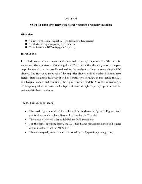
MOSFET High Frequency Model and Amplifier Frequency Response
MOSFET High Frequency Model and Amplifier Frequency Response
MOSFET High Frequency Model and Amplifier Frequency Response

Create successful ePaper yourself
Turn your PDF publications into a flip-book with our unique Google optimized e-Paper software.
Lecture 3B<br />
<strong>MOSFET</strong> <strong>High</strong> <strong>Frequency</strong> <strong>Model</strong> <strong>and</strong> <strong>Amplifier</strong> <strong>Frequency</strong> <strong>Response</strong><br />
Objectives<br />
• To review the small signal BJT models at low frequencies<br />
• To study the high frequency BJT models<br />
• To estimate the BJT unity-gain frequency<br />
Introduction<br />
In the last two lectures we examined the time <strong>and</strong> frequency response of the STC circuits.<br />
As we said the importance of studying the STC circuits is that the analysis of a complex<br />
amplifier circuit can be usually reduced to the analysis of one or more simple STC<br />
circuits. The frequency response of the amplifier circuits will be explored starting next<br />
lecture. Before starting this study it will be constructive to review in this lecture the BJT<br />
small-signal models, <strong>and</strong> examining the high-frequency models. Also, the transistor cutoff<br />
frequency which is considered a figure of merit at high frequency operation will be<br />
estimated for both transistors.<br />
The BJT small-signal model<br />
• The small signal model of the BJT amplifier is shown in figure 5. Figures 5-a,b<br />
are for the π-model, where Figures 5-c,d are for the T-model.<br />
• These models are valid for both NPN <strong>and</strong> PNP transistors.<br />
• For the same operating point, the BJT has higher transconductance <strong>and</strong> higher<br />
output resistance that the <strong>MOSFET</strong>.<br />
• The small-signal parameters are controlled by the Q-point (operating point).
gm Vπ<br />
Figure 1 small signal-models of the BJT<br />
• The BJT small-signal parameters may be summarized in Table 3<br />
Table 1 BJT small signal parameters<br />
Symbol Parameter Value<br />
g m<br />
r π<br />
r e<br />
Transconductance<br />
Base input resistance<br />
Emitter input resistance<br />
g<br />
m<br />
I<br />
=<br />
V<br />
V T is the thermal voltage = kT/q, which<br />
equals 25mV at room temperature.<br />
k is Boltzman's constant<br />
T is the absolute temperature in<br />
Kelvins<br />
q is the electron charge<br />
VT<br />
VT<br />
β<br />
rπ<br />
= = β ⎛<br />
⎜<br />
⎞<br />
⎟=<br />
I<br />
B ⎝IC<br />
⎠ g m<br />
β is the common-emitter current gain<br />
VT<br />
VT<br />
α<br />
re<br />
= = α ⎛<br />
⎜<br />
⎞<br />
⎟=<br />
I<br />
E ⎝IC<br />
⎠ g m<br />
α is the common-base current gain<br />
C<br />
T
Symbol Parameter Value<br />
r o<br />
Output resistance<br />
r<br />
V + V V<br />
A CE A<br />
= <br />
o<br />
IC<br />
IC<br />
V A is the early voltage.<br />
The BJT high-frequency model:<br />
Figure 2 The high-frequency hybrid- π model of the BJT<br />
• The high frequency hybrid-π model for the BJT is shown in Figure 6.<br />
• This model is useful for signal frequencies up to a several tens of megahertz, after<br />
which a more detailed model becomes necessary.<br />
• Typically, the base-emitter junction capacitance C π is in the range of few pF to<br />
few tens of pF, while the collector-base junction capacitance C μ is in the range of<br />
fraction of pF to few pF<br />
• The base resistor r x is added partly to account for the comparatively long internal<br />
connection from the base external connection <strong>and</strong> the actual internal base<br />
connection.<br />
• A representative resistance value for this lumped resistor is in the range of 50Ω to<br />
perhaps 200Ω.<br />
• This resistor ordinarily can be neglected for h<strong>and</strong> estimates.<br />
• Note that r x becomes the dominant input resistance for frequencies so high that C π<br />
effectively short-circuits r π .
• A second base-width modulation effect, characterized by a resistor connected<br />
between the base <strong>and</strong> collector is omitted; its influence is dominated by the<br />
collector junction reverse-bias capacitance C μ .<br />
• The emitter junction (diffusion) capacitance C π represents the charge store to<br />
support the current flow across the base.<br />
The BJT Cutoff frequency:<br />
• As defined earlier, it is the frequency at which the current gain of the transistor<br />
becomes one. (i.e. no more active element). It is calculated by finding the short<br />
circuit collector current in terms of the base current.<br />
• Using the high frequency model of BJT we can draw the circuit to estimate the<br />
cut-off frequency of the BJT as shown in Figure 7.<br />
sC μ<br />
V π I = ( g −sC ) V<br />
c<br />
m<br />
μ<br />
π<br />
Figure 3 Circuit used to estimate the BJT cutoff frequency<br />
• Applying nodal analysis at the input <strong>and</strong> output nodes as we did earlier. We can<br />
estimate the cut-off frequency as follows:<br />
V<br />
π<br />
I<br />
b<br />
= + sC V + sC V<br />
rπ<br />
V<br />
π<br />
I<br />
b<br />
= + sC (<br />
π<br />
+ Cμ ) Vπ<br />
r<br />
h<br />
π<br />
I<br />
c<br />
fe<br />
≡ =<br />
I<br />
b<br />
π π μ π<br />
gm<br />
− sCμ<br />
1<br />
+ sC (<br />
π<br />
+ Cμ<br />
)<br />
r<br />
π
Assuming gm<br />
Assuming<br />
h<br />
fe<br />
∴<br />
>> sC μ<br />
⇒<br />
h<br />
fe<br />
gm<br />
rπ<br />
≅<br />
1 + sC ( + C ) r<br />
π μ π<br />
gmrπ<br />
gm<br />
>> sCμ<br />
⇒ hfe<br />
≅<br />
1 + sC ( + C ) r<br />
βo<br />
1<br />
≅ where ωp<br />
=<br />
s<br />
1+<br />
( C + C ) r<br />
ω<br />
p<br />
Unity gain b<strong>and</strong>width<br />
g<br />
m<br />
( ωT ) = βoωp<br />
=<br />
( C + C )<br />
π<br />
μ<br />
π μ π<br />
π μ π<br />
h<br />
h<br />
h<br />
c<br />
fe<br />
≡ =<br />
I<br />
b<br />
fe<br />
fe<br />
I<br />
1<br />
r<br />
m<br />
+ sC ( + C )<br />
gm<br />
rπ<br />
≅ assuming gm<br />
> > sC<br />
1 + sC ( + C ) r<br />
βo<br />
1<br />
≅ where ωp<br />
=<br />
s<br />
1+<br />
( C + C ) r<br />
ω<br />
p<br />
π<br />
g<br />
− sC<br />
π<br />
π μ π<br />
μ<br />
μ<br />
π μ π<br />
g<br />
m<br />
∴ Unity gain b<strong>and</strong>width ( ωT ) = βoωp<br />
=<br />
( C + C )<br />
π<br />
μ<br />
μ<br />
• We can observe from the last analysis that the common-emitter current gain (h fe )<br />
frequency response is similar to a simple pole with ω p as the pole frequency. This<br />
may be drawn as shown in Figure 8
|h fe | [dB]<br />
β o<br />
3 dB<br />
-6 dB/octave<br />
0 dB<br />
β<br />
T<br />
[log scale]<br />
Figure 4 Bode plot of |h fe |<br />
• As we can see from the last equation. <strong>High</strong>er ω T means higher g m <strong>and</strong> lower<br />
internal BJT capacitances which means better amplifier operation.<br />
• Typically, f T is ranging from about 100MHz to Tens of GHz.