Crown Low Power Transmitters - Crown Broadcast
Crown Low Power Transmitters - Crown Broadcast
Crown Low Power Transmitters - Crown Broadcast

You also want an ePaper? Increase the reach of your titles
YUMPU automatically turns print PDFs into web optimized ePapers that Google loves.
®<br />
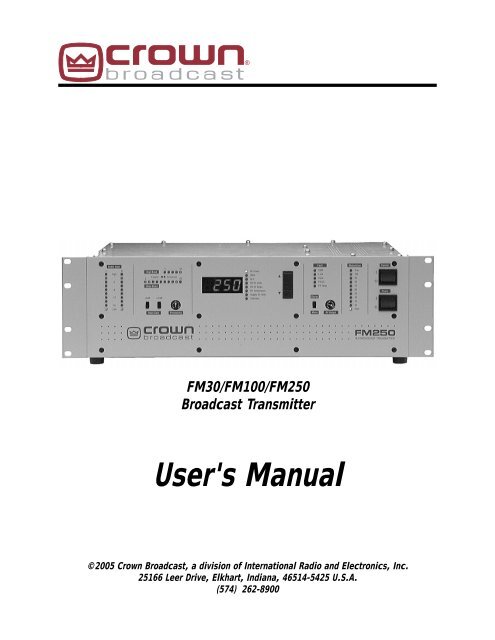
FM30/FM100/FM250<br />
<strong>Broadcast</strong> Transmitter<br />
User's Manual<br />
©2005 <strong>Crown</strong> <strong>Broadcast</strong>, a division of International Radio and Electronics, Inc.<br />
25166 Leer Drive, Elkhart, Indiana, 46514-5425 U.S.A.<br />
(574) 262-8900<br />
i
Revision Control<br />
Revision<br />
Print Date<br />
Initial Release (Rev. 0; K80620–6) February 1995<br />
Revision 1 (K80664–4) November 1995<br />
Revision 2 (K80664A2) March 1996<br />
Revision 3 (100885–1) October 1996<br />
Revision 4 (100885–2) July 1997<br />
Revision 5 (900194-1) October 1997<br />
Revision 6 (130758-1) April 2000<br />
Revision 7 April 2002<br />
Revision 8 April 2005<br />
Important Notices<br />
©2005, <strong>Crown</strong> <strong>Broadcast</strong>, a division of International Radio and Electronics, Inc.<br />
Portions of this document were originally copyrighted by Michael P. Axman in 1991.<br />
All rights reserved. No part of this publication may be reproduced, transmitted,<br />
transcribed, stored in a retrieval system, or translated into any language in any<br />
form by any means without the written permission of <strong>Crown</strong> International, Inc.<br />
Printed in U.S.A.<br />
<strong>Crown</strong> attempts to provide information that is accurate, complete, and useful.<br />
Should you find inadequacies in the text, please send your comments to the following<br />
address:<br />
International Radio and Electronics<br />
25166 Leer Drive, P.O. Box 2000<br />
Elkhart, Indiana, 46515-2000 U.S.A.<br />
ii
Contents<br />
Section 1—Getting Acquainted ..................................... 1–1<br />
1.1 Your Transmitter ............................................................................................... 1–2<br />
1.2 Applications and Options................................................................................... 1–3<br />
1.2.1 Stand-Alone .................................................................................................. 1–4<br />
1.2.2 Backup .......................................................................................................... 1–4<br />
1.2.3 Booster ......................................................................................................... 1–4<br />
1.2.4 Exciter........................................................................................................... 1–4<br />
1.2.5 Translator...................................................................................................... 1–5<br />
1.2.6 Satellator ...................................................................................................... 1–6<br />
1.2.7 Nearcasting ................................................................................................... 1–6<br />
1.3 Transmitter/Exciter Specifications ..................................................................... 1–7<br />
1.4 Receiver Specifications ..................................................................................... 1–9<br />
1.5 Safety Considerations...................................................................................... 1–10<br />
1.5.1 Dangers ...................................................................................................... 1–10<br />
1.5.2 Warnings .................................................................................................... 1–10<br />
1.5.3 Cautions...................................................................................................... 1–10<br />
Section 2—Installation ............................................... 2–1<br />
2.1 Operating Environment...................................................................................... 2–2<br />
2.2 <strong>Power</strong> Connections ........................................................................................... 2–2<br />
2.2.1 AC Line Voltage Setting ................................................................................ 2–2<br />
2.2.2 Fuses ............................................................................................................ 2–4<br />
2.2.3 Battery <strong>Power</strong> ............................................................................................... 2–5<br />
2.3 Frequency (Channel) Selection .......................................................................... 2–5<br />
2.3.1 Modulation Compensator .............................................................................. 2–7<br />
2.4 Receiver Frequency Selection ............................................................................ 2–7<br />
2.5 RF Connections ............................................................................................... 2–10<br />
2.6 Audio Input Connections ................................................................................. 2–11<br />
2.7 SCA Input Connections ................................................................................... 2–12<br />
2.8 Composite Input Connection ........................................................................... 2–12<br />
2.9 Audio Monitor Connections ............................................................................. 2–13<br />
2.10 Pre-emphasis Selection ................................................................................... 2–13<br />
2.11 Program Input Fault Time-out...........................................................................2–14<br />
2.12 Remote I/O Connector.....................................................................................2–14<br />
iii
Section 3—Operation ................................................. 3–1<br />
3.1 Initial <strong>Power</strong>-up Procedures .............................................................................. 3–2<br />
3.2 <strong>Power</strong> Switches................................................................................................. 3–4<br />
3.2.1 DC Breaker.................................................................................................... 3–4<br />
3.2.2 <strong>Power</strong> Switch ................................................................................................ 3–4<br />
3.2.3 Carrier Switch ............................................................................................... 3–4<br />
3.3 Front Panel Bar-Dot Displays ............................................................................. 3–5<br />
3.3.1 Audio Processor Input .................................................................................. 3–5<br />
3.3.2 Highband and Wideband Display .................................................................. 3–5<br />
3.3.3 Modulation Display ....................................................................................... 3–5<br />
3.4 Input Gain Switches .......................................................................................... 3–6<br />
3.5 Processing Control ............................................................................................ 3–6<br />
3.6 Stereo-Mono Switch.......................................................................................... 3–6<br />
3.7 RF Output Control ............................................................................................. 3–7<br />
3.8 Digital Multimeter .............................................................................................. 3–7<br />
3.9 Fault Indicators ................................................................................................. 3–8<br />
Section 4—Principles of Operation................................. 4–1<br />
4.1 Part Numbering ................................................................................................. 4–2<br />
4.2 Audio Processor Circuit Board .......................................................................... 4–3<br />
4.3 Stereo Generator Circuit Board.......................................................................... 4–4<br />
4.4 RF Exciter Circuit Board .................................................................................... 4–6<br />
4.5 Metering Circuit Board ...................................................................................... 4–8<br />
4.6 Motherboard ..................................................................................................... 4–9<br />
4.7 Display Circuit Board ....................................................................................... 4–10<br />
4.8 Voltage Regulator Circuit Board ...................................................................... 4–11<br />
4.9 <strong>Power</strong> Regulator Circuit Board ........................................................................ 4–12<br />
4.10 RF Driver/Amplifier (FM30) ............................................................................. 4–12<br />
4.11 RF Driver (FM100/FM250)............................................................................... 4–13<br />
4.12 RF Amplifier (FM100/FM250) .......................................................................... 4–13<br />
4.13 Chassis ........................................................................................................... 4–14<br />
4.14 RF Output Filter & Reflectometer..................................................................... 4–14<br />
4.15 Receiver Circuit Board Option ......................................................................... 4–15<br />
iv
Section 5—Adjustments and Tests ................................. 5–1<br />
5.1 Audio Processor Adjustments ........................................................................... 5–2<br />
5.1.1 Pre-Emphasis Selection ................................................................................ 5–2<br />
5.1.2 Pre-Emphasis Fine Adjustment ..................................................................... 5–2<br />
5.2 Stereo Generator Adjustments .......................................................................... 5–2<br />
5.2.1 Separation .................................................................................................... 5–2<br />
5.2.2 Composite Output ......................................................................................... 5–2<br />
Using a Modulation Monitor 5–3<br />
5.2.3 19–kHz Level ................................................................................................ 5–4<br />
5.2.4 19–kHz Phase ............................................................................................... 5–4<br />
5.3 Frequency Synthesizer Adjustments .................................................................. 5–4<br />
5.3.1 Frequency (Channel) Selection ...................................................................... 5–4<br />
5.3.2 Modulation Compensator .............................................................................. 5–4<br />
5.3.3 Frequency Measurement and Adjustment ..................................................... 5–4<br />
5.3.4 FSK Balance Control ..................................................................................... 5–5<br />
5.4 Metering Board Adjustments ............................................................................. 5–5<br />
5.4.1 <strong>Power</strong> Calibrate............................................................................................. 5–5<br />
5.4.2 <strong>Power</strong> Set ..................................................................................................... 5–5<br />
5.4.3 SWR Calibrate............................................................................................... 5–5<br />
5.4.4 PA Current Limit ........................................................................................... 5–6<br />
5.5 Motherboard Adjustments ................................................................................. 5–6<br />
5.6 Display Modulation Calibration .......................................................................... 5–6<br />
5.7 Voltage Regulator Adjustments ......................................................................... 5–6<br />
5.8 Bias Set (RF <strong>Power</strong> Amplifier) ........................................................................... 5–7<br />
5.9 Performance Verification ................................................................................... 5–7<br />
5.9.1 Audio Proof-of-Performance Measurements ................................................. 5–7<br />
5.9.2 De-emphasis Input Network.......................................................................... 5–7<br />
5.10 Carrier Frequency .............................................................................................. 5–8<br />
5.11 Output <strong>Power</strong> .................................................................................................... 5–8<br />
5.12 RF Bandwidth and RF Harmonics ...................................................................... 5–8<br />
5.13 Pilot Frequency ................................................................................................. 5–8<br />
5.14 Audio Frequency Response ............................................................................... 5–9<br />
5.15 Audio Distortion ................................................................................................ 5–9<br />
5.16 Modulation Percentage...................................................................................... 5–9<br />
5.17 FM and AM Noise .............................................................................................. 5–9<br />
5.18 Stereo Separation .............................................................................................. 5–9<br />
5.19 Crosstalk ........................................................................................................... 5–9<br />
5.19.1 Main Channel Into Sub .............................................................................. 5–10<br />
5.19.2 Sub Channel Into Main .............................................................................. 5–10<br />
5.20 38–kHz Subcarrier Suppression ...................................................................... 5–10<br />
5.21 Additional Checks ............................................................................................ 5–10<br />
v
Section 6—Reference Drawings .................................... 6–1<br />
6.1 Views ................................................................................................................ 6–2<br />
6.2 Board Layouts and Schematics ......................................................................... 6–4<br />
Section 7—Service and Support .................................... 7–1<br />
7.1 Service .............................................................................................................. 7–2<br />
7.2 24–Hour Support .............................................................................................. 7–2<br />
7.3 Spare Parts ....................................................................................................... 7–2<br />
Transmitter Output Efficiency .............................. Appendix–1<br />
Glossary ................................................................. G–1<br />
Index................................................................ Index–1<br />
vi
I<br />
INFORMATION<br />
Section 1—Getting Acquainted<br />
This section provides a general description of the FM30, FM100,<br />
and FM250 transmitters and introduces you to safety conventions<br />
used within this document. Review this material before installing<br />
or operating the transmitter.<br />
Getting Acquainted<br />
1–1
I<br />
1.1 Your Transmitter<br />
The FM30, FM100, and FM250 are members of a family of FM stereo broadcast<br />
transmitters. <strong>Crown</strong> transmitters are known for their integration, ease-of-use, and<br />
reliability.<br />
The integration is most apparent in the standard transmitter configuration which<br />
incorporates audio processing, stereo generation, and RF amplification without<br />
compromised signal quality. A single <strong>Crown</strong> transmitter can replace several pieces<br />
of equipment in a traditional system.<br />
Ease-of-use is apparent in the user-friendly front panel interface and in the installation<br />
procedure. Simply select your operating frequency (using 4 internal<br />
switches), add an audio source, attach an antenna, and connect AC or DC power<br />
and you're ready to broadcast. Of course, the FM series of transmitters also feature<br />
more sophisticated inputs and monitoring connections if needed.<br />
Reliability is a <strong>Crown</strong> tradition. The first <strong>Crown</strong> transmitters were designed for<br />
rigors of worldwide and potentially portable use. The modular design, quality<br />
components, engineering approach, and high production standards ensure stable<br />
performance.<br />
Remote control and metering of the transmitter is made possible through a builtin<br />
I/O port. For more direct monitoring, the front panel includes a digital multimeter<br />
display and status indicators. Automatic control circuitry provides protection<br />
for high VSWR as well as high current, voltage, and temperature conditions.<br />
Illustration 1–1 FM250 Stereo <strong>Broadcast</strong> Transmitter<br />
This manual describes the FM30, FM100, and FM250 because all three transmitters<br />
share common design factors. Specific product differences are noted throughout<br />
the manual. In physical appearance, the FM30 differs from the FM100 and<br />
FM250 in that it lacks the power amplifier and cooling fan assembly on the back<br />
panel.<br />
1–2 FM30/FM100/FM250 User's Manual
1.2 Applications and Options<br />
<strong>Crown</strong> transmitters are designed for versatility in applications. They have been used<br />
as stand-alone and backup transmitters and in booster, translator, satellator, and<br />
nearcast applications. The following discussion describes these applications further.<br />
Model numbers describe the configuration of the product (which has to do with its<br />
intended purpose) and the RF output power which you can expect.<br />
The number portion of each name represents the maximum RF output power. The<br />
FM250, for example, can generate up to 250 watts of RF output power.<br />
Suffix letters describe the configuration. The FM250T, for example, is the standard<br />
or transmitter configuration. Except where specified, this document describes the<br />
transmitter configuration. In this configuration, the product includes the following<br />
components (functions):<br />
❑<br />
❑<br />
❑<br />
❑<br />
❑<br />
audio processor<br />
stereo generator<br />
RF exciter<br />
metering<br />
low-pass filter<br />
RF Exciter<br />
Stereo<br />
Generator<br />
<strong>Low</strong>-pass<br />
Filtering<br />
Audio<br />
Processor<br />
Metering<br />
®<br />
FM250<br />
Illustration 1–2 Standard (Transmitter) Configuration<br />
Getting Acquainted<br />
1–3
I<br />
1.2.1 Stand-Alone<br />
In the standard configuration, the FM30, FM100, and FM250 are ideal stand-alone<br />
transmitters. When you add an audio source (monaural, L/R stereo, or composite<br />
signal), an antenna, and AC or DC power, the transmitter becomes a complete FM<br />
stereo broadcast station, capable of serving a community.<br />
As stand-alone transmitters, <strong>Crown</strong> units often replace multiple pieces of equipment<br />
in a traditional setup (exciter, audio processor, RF amplifier).<br />
1.2.2 Backup<br />
In the standard configuration, <strong>Crown</strong> transmitters are also used in backup applications.<br />
Should your primary transmitter become disabled, you can continue to<br />
broadcast while repairs take place. In addition, the FM transmitters can replace<br />
disabled portions of your existing system including the exciter, audio processor, or<br />
amplifier. Transfer switches on each side of the existing and backup transmitters<br />
make the change-over possible with minimal downtime.<br />
The DC operation option of the FM30, FM100, and FM250 make them attractive<br />
backup units for those times when AC power is lost.<br />
1.2.3 Booster<br />
Also in the standard configuration, <strong>Crown</strong> transmitters have been used as booster<br />
transmitters. Booster applications typically involve certain geographic factors<br />
which prevent your system from broadcasting to the full coverage area allowable.<br />
For example, a mountain range might block your signal to a portion of your<br />
coverage area. Careful placement of a <strong>Crown</strong> transmitter, operating on the same<br />
frequency as your primary transmitter, can help you reach full coverage.<br />
1.2.4 Exciter<br />
In addition to the standard configuration, the FM30, FM100, and FM250 are<br />
available in optional configurations to meet a variety of needs.<br />
An "E" suffix, as in the FM30E, for example, represents an exciter-only configuration.<br />
In this configuration, the audio processor and stereo generator boards are<br />
replaced with circuitry to bypass their function. The exciter configurations are the<br />
least expensive way to get <strong>Crown</strong>-quality components into your transmission<br />
system.<br />
You might consider the <strong>Crown</strong> exciter when other portions of your system are<br />
performing satisfactorily and you want to maximize your investment in present<br />
equipment.<br />
1–4 FM30/FM100/FM250 User's Manual
1.2.5 Translator<br />
A receiver configuration (FM100R, for example) replaces the audio processor and<br />
stereo generator boards with a receiver module. This added feature makes the<br />
FM30, FM100, and FM250 ideal for translator service in terrestrial-fed networks.<br />
These networks represent a popular and effective way to increase your broadcasting<br />
coverage. Translators, acting as repeater emitters, are necessary links in this chain<br />
of events.<br />
Traditionally, network engineers have relied on multiple steps and multiple pieces<br />
of equipment to accomplish the task. Others have integrated the translator<br />
function (receiver and exciter) to feed an amplifier. <strong>Crown</strong>, on the other hand,<br />
starts with an integrated transmitter and adds a solid-state Receiver Module to<br />
form the ideal translator.<br />
Receiver<br />
Module<br />
(option)<br />
Frequency<br />
Selection<br />
RF In<br />
<strong>Low</strong>-pass<br />
Filter<br />
RF Out<br />
RF Exciter<br />
Metering<br />
®<br />
FM250<br />
Illustration 1–3 <strong>Crown</strong>'s Integrated Translator<br />
This option enables RF in and RF out on any of <strong>Crown</strong>’s FM series of transmitters.<br />
In addition, the module supplies a composite output to the RF exciter portion of<br />
the transmitter. From here, the signal is brought to full power by the built-in<br />
power amplifier for retransmission. The Receiver Module has been specifically<br />
designed to handle SCA channel output up to 100 kHz for audio and high-speed<br />
data.<br />
FSK ID programming is built-in to ensure compliance with FCC regulations<br />
regarding the on-air identification of translators. Simply specify the call sign of<br />
the repeater station when ordering. Should you need to change the location of the<br />
translator, replacement FSK chips are available. The Receiver Module option<br />
should be ordered at the time of initial transmitter purchase. However, an option<br />
kit is available for field converting existing <strong>Crown</strong> units.<br />
In the translator configuration there are differences in the function of the front<br />
panel, see Section 3 for a description.<br />
Getting Acquainted<br />
1–5
I<br />
1.2.6 Satellator<br />
One additional option is available for all configurations—an FSK Identifier (FSK<br />
IDer). This added feature enables the FM30, FM100, and FM250 to transmit its<br />
call sign or operating frequency in a Morse code style. This option is intended for<br />
use in satellite-fed networks. <strong>Transmitters</strong> equipped in this fashion are often<br />
known as "satellators."<br />
Connect the transmitter to your satellite receiver and the pre-programmed FSK<br />
IDer does the rest—shifting the frequency to comply with FCC requirements and<br />
in a manner that is unnoticeable to the listener. The FSK IDer module should be<br />
ordered at the time you order your transmitter, but is available separately (factory<br />
programmed for your installation).<br />
<strong>Low</strong>-pass<br />
Filter<br />
RF Out<br />
Stereo<br />
Generator<br />
RF Exciter<br />
Audio<br />
Processor<br />
Metering<br />
®<br />
FM250<br />
Illustration 1–4 Transmitter with FSK IDer Option<br />
Add the FSK IDer option to the exciter configuration for the most economical<br />
satellator (a composite input signal is required).<br />
1.2.7 Nearcasting<br />
The output power of an FM30 transmitter Can be reduced to a level that could<br />
Function as a near-cast transmitter. <strong>Crown</strong> transmitters have been used in this<br />
way for language translation, for rebroadcasting the audio of sporting events within<br />
a stadium, and for specialized local radio. The FM30 is the only transmitter that is<br />
appropriate for this application.<br />
1–6 FM30/FM100/FM250 User's Manual
1.3 Transmitter/Exciter Specifications<br />
Frequency Range<br />
RF <strong>Power</strong> Output<br />
FM30<br />
FM100<br />
FM250<br />
RF Output Impedance<br />
Frequency Stability<br />
Audio Input Impedance<br />
Audio Input Level<br />
Pre-emphasis<br />
Audio Response<br />
Complete transmitter<br />
87.9 MHz–108 MHz (76 MHz–90 MHz<br />
optionally available)<br />
(VSWR 1.5:1 or better)<br />
3 - 30 watts, adjustable<br />
10 - 100 watts, adjustable<br />
20 - 250 watts, adjustable<br />
50 Ω<br />
Meets FCC specifications from<br />
0-50 degrees C<br />
50 kΩ bridging, balanced, or 600 Ω<br />
Selectable for –10 dBm to +10 dBm for<br />
75 kHz deviation at 400 Hz<br />
Selectable for 25, 50, or 75 µsec; or<br />
Flat<br />
Conforms to 75 µsec pre-emphasis<br />
curve as follows<br />
±0.30 dB (50 Hz–10 kHz)<br />
±1.0 dB (10 kHz–15 kHz)<br />
Exciter only<br />
±0.25 dB (50 Hz–15 kHz)<br />
Distortion (THD + Noise)<br />
Complete transmitter<br />
Exciter only<br />
Less than 0.7% (at 15 kHz)<br />
Less than 0.3% (50 Hz–15 kHz)<br />
Stereo Separation<br />
Complete transmitter<br />
Exciter only<br />
Crosstalk<br />
Better than –40 dB (50 Hz–15 kHz)<br />
Better than –40 dB (50 Hz–15 kHz)<br />
Main into sub, better than –40 dB<br />
Sub into main, better than –40 dB<br />
Stereo Pilot<br />
19 kHz ±2 Hz, 9% modulation<br />
Getting Acquainted<br />
1–7
I<br />
Subcarrier Suppression<br />
FM S/N Ratio (FM noise)<br />
Complete transmitter<br />
Exciter only<br />
AM S/N Ratio<br />
RF Bandwidth<br />
RF Spurious Products<br />
50 dB below ±75 kHz deviation<br />
Better than –60 dB<br />
Better than –70 dB<br />
Asynchronous and synchronous noise<br />
better than FCC requirements<br />
±120 kHz, better than –35 dB<br />
±240 kHz, better than –45 dB<br />
Better than –70 dB<br />
Operating Environment Temperature (0 o C –50 o C)<br />
Humidity (0–80% at 20 o C)<br />
Maximum Altitude (3,000 meters; 9843<br />
feet)<br />
AC <strong>Power</strong> 100, 120, 220, or 240 volts (+10%/<br />
–15%); 50/60 Hz<br />
FM30<br />
FM100<br />
FM250<br />
115 VA<br />
297 VA<br />
550 VA<br />
DC <strong>Power</strong><br />
FM30<br />
FM100 and FM250<br />
24–36 volts (36 volts at 3 amps required for<br />
full output power)<br />
36–62 volts [48 volts at 5 amps (FM100) or<br />
72 volts at 8 amps (FM250) required for<br />
full output power]<br />
1–8 FM30/FM100/FM250 User's Manual
Note: We set voltage and ampere requirements to assist you in designing your<br />
system. Depending on your operating frequency, actual requirements for maximum<br />
voltage and current readings are 10–15% lower than stated.<br />
Regulatory Type notified for FCC parts 73 and 74<br />
Meets FCC, DOC, and CCIR requirements<br />
Dimensions<br />
Weight<br />
FM30<br />
FM100<br />
FM250<br />
13.5 x 41.9 x 44.5 cm<br />
(5.25 x 16.5 x 17.5 inches)<br />
10.5 kg (23 lbs)<br />
13.6 kg (30 lbs) shipping weight<br />
11.4 kg (25 lbs)<br />
14.5 kg (32 lbs) shipping weight<br />
16.8 kg (37 lbs)<br />
20.0 kg (44 lbs) shipping weight<br />
Getting Acquainted<br />
1–9
I<br />
1.4 Receiver Specifications<br />
Monaural Sensitivity (demodulated, de-emphasized)<br />
3.5 µV for signal-to-noise > 50 dB<br />
Stereo Sensitivity (19–kHz pilot frequency added)<br />
31 µ V for signal-to-noise > 50 dB<br />
Connector Standard type N, 50 Ω<br />
Shipping Weight 1 lb<br />
1.5 Safety Considerations<br />
<strong>Crown</strong> <strong>Broadcast</strong> assumes the responsibility for providing you a safe product and<br />
safety guidelines during its use. “Safety” means protection to all individuals who<br />
install, operate, and service the transmitter as well as protection of the transmitter<br />
itself. To promote safety, we use standard hazard alert labeling on the product and<br />
in this manual. Follow the associated guidelines to avoid potential hazard.<br />
1.5.1 Dangers<br />
DANGER represents the most severe hazard alert. Extreme bodily harm or death<br />
will occur if DANGER guidelines are not followed.<br />
1.5.2 Warnings<br />
WARNING represents hazards which could result in severe injury or death.<br />
1.5.3 Cautions<br />
CAUTION indicates potential personal injury, or equipment or property damage if<br />
the associated guidelines are not followed. Particular cautions in this text also<br />
indicate unauthorized radio-frequency operation.<br />
WARNING<br />
Severe shock hazard!<br />
Type of Hazard<br />
Pictorial Indication<br />
of Hazard<br />
Turn power off and<br />
wait approximately 1<br />
minute for capacitors<br />
to discharge before<br />
handling them.<br />
Illustration 1–5 Sample Hazard Alert<br />
Explanation<br />
of Hazard<br />
1–10 FM30/FM100/FM250 User's Manual
®<br />
Section 2—Installation<br />
This section provides important guidelines for installing your transmitter.<br />
Review this information carefully for proper installation.<br />
Installation<br />
2–1
CAUTION<br />
Possible equipment damage!<br />
Before operating the transmitter for<br />
the first time, check for the proper AC<br />
line voltage setting and frequency<br />
selection as described in sections 2.2<br />
and 2.3.<br />
2.1 Operating Environment<br />
You can install the FM transmitter in a standard component rack or on a suitable<br />
surface such as a bench or desk. In any case, the area should be as clean and wellventilated<br />
as possible. Always allow for at least 2 cm of clearance under the unit for<br />
ventilation. If you set the transmitter on a flat surface, install spacers on the<br />
bottom cover plate. If you install the transmitter in a rack, provide adequate<br />
clearance above and below. Do not locate the transmitter directly above a hot piece<br />
of equipment.<br />
2.2 <strong>Power</strong> Connections<br />
The FM30, FM100, and FM250 operate on 100, 120, 220, or 240 volts AC (50 or 60<br />
Hz; single phase). Each transmitter can operate on DC power as well (28 volts for<br />
the FM30, 36 volts for the FM100, and 62 volts for the FM250). The transmitter<br />
can operate on fewer volts DC, but with reduced RF output power (see section 1.2).<br />
In addition, the transmitter isolates the AC and DC sources; both can be connected<br />
at the same time to provide battery backup in the event of an AC power failure.<br />
2.2.1 AC Line Voltage Setting<br />
To change the voltage setting, follow these steps:<br />
1. Disconnect the power cord if it is attached.<br />
2. Open the cover of the power connector assembly using a small, flat blade<br />
screwdriver. See Illustration 2–1.<br />
3. Insert the screwdriver into the voltage selection slot and remove the drum<br />
from the assembly.<br />
4. Rotate the drum to select the desired voltage. See Illustration 2–2.<br />
5. Replace the drum and cover and check to see that the correct voltage appears<br />
in the connector window.<br />
6. Connect the AC power cord.<br />
2–2 FM30/FM100/FM250 User's Manual
120Vac<br />
Illustration 2–1 Removing the <strong>Power</strong> Connector Cover<br />
remove drum<br />
before turn<br />
120Vac<br />
220Vac<br />
240Vac<br />
Illustration 2–2 Selecting an AC Line Voltage<br />
Installation<br />
2–3
2.2.2 Fuses<br />
The fuse holders are located in the power connector assembly just below the voltage<br />
selector.<br />
120Vac<br />
220Vac<br />
240Vac<br />
remove drum<br />
before turn<br />
Illustration 2–3 Fuse Holder<br />
For 100 to 120 VAC operation, use the fuse installed at the factory. For 220 to 240<br />
VAC operation, use the slow-blow fuse located in a hardware kit within the<br />
transmitter packaging. Consult the following table:<br />
Transmitter Input <strong>Power</strong> Fuse<br />
FM30 100–120 V 3 A<br />
220–240 V 1.5 A<br />
FM100 100–120 V 6.3 A<br />
220–240 V 4 A<br />
FM250 100–120 V 12.5 A<br />
220–240 V 6.3 A<br />
Illustration 2–4 Fuse Reference Table<br />
2–4 FM30/FM100/FM250 User's Manual
2.2.3 Battery <strong>Power</strong><br />
Your transmitter can operate on a DC power source (such as 3 or 4, 12–volt automotive<br />
batteries connected in series). The FM30 requires 28 volts DC for full<br />
output power, while the FM100 requires 36 volts, and FM250 requires 62 volts for<br />
full output power. Connect the batteries to the red (+) and black (–) battery input<br />
binding posts on the rear panel.<br />
SCA IN COMPOSITE IN MONITOR<br />
RIGHT<br />
LEFT/MONO<br />
R<br />
L<br />
REMOTE I/O<br />
1<br />
2 3<br />
DC Input Terminals<br />
CIRCUIT<br />
BREAKER<br />
OFF<br />
+<br />
–<br />
B<br />
A<br />
T<br />
T<br />
E<br />
R<br />
Y<br />
36 VDC<br />
Illustration 2–5 DC Input Terminals<br />
CAUTION<br />
Possible equipment damage!<br />
Never connect a battery charger to the<br />
input terminals of the transmitter<br />
unless a battery is also connected.<br />
Voltage peaks from a typical charger<br />
(without the load of a battery) can be<br />
destructive to the transmitter.<br />
2.3 Frequency (Channel) Selection<br />
You may select an operating frequency of 87 to 108 MHz in the FM broadcast band.<br />
Pins 9 and 10 of HD2 on the RF Exciter board are jumpered for frequencies<br />
other than these such as the optional Japan frequencies of 76-90 MHz.<br />
To adjust the operating frequency, follow these steps:<br />
1. Remove the top cover by removing 18 screws.<br />
Installation<br />
2–5
2. Locate the RF Exciter board and identify the frequency selector switches<br />
which will be used to change the setting. See Illustrations 2–6 and 2–7.<br />
Modulation<br />
Trim-pot<br />
Frequency Selection<br />
Rotary Switches<br />
RF Exciter<br />
®<br />
FM250<br />
Illustration 2–6 Top Cover Removed<br />
OPTIONAL<br />
MEGAHERTZ .1 .01<br />
Illustration 2–7 RF Exciter Board (Frequency Selector Switches)<br />
3. Use small flat blade screwdriver or another suitable device to rotate the<br />
switches to the desired setting. (The selected number will appear directly<br />
above the white indicator dot on each switch.) See examples of selected<br />
frequencies in the illustration below.<br />
= 88.1 MHz<br />
= 107.9 MHz<br />
Illustration 2–8 Two Sample Frequency Selections<br />
2–6 FM30/FM100/FM250 User's Manual
2.3.1 Modulation Compensator<br />
The Modulation trim-potentiometer (see illustration 2–6) compensates for slight<br />
variations in deviation sensitivity with frequency. Set the trim-pot dial according to<br />
the following graph:<br />
Modulation Compensation Pot Setting<br />
90<br />
80<br />
70<br />
60<br />
50<br />
40<br />
30<br />
20<br />
10<br />
0<br />
75 80 85 90 95 100 105 110<br />
Frequency (MHz)<br />
Illustration 2–9 Modulation Compensator Settings<br />
These compensator settings are approximate. Each mark on the potentiometer<br />
represents about 1.8% modulation compensation. For more exact settings, refer to<br />
section 5.2.2.<br />
Installation<br />
2–7
2.4 Receiver Frequency Selection<br />
If you have a transmitter equipped with the receiver option, you will need to set the<br />
receiving or incoming frequency.<br />
1. With the top cover removed, locate the receiver module and the two switches<br />
(labeled SW1 and SW2).<br />
Receiver<br />
Module<br />
Frequency Selection Switches<br />
®<br />
FM250<br />
Illustration 2–10 Receiver Module Switches<br />
2. Use the adjacent chart to set the switches for the desired incoming frequency.<br />
3. After setting the frequency, replace the top cover and screws.<br />
2–8 FM30/FM100/FM250 User's Manual
Frequency<br />
SW1 SW2<br />
87.9 0 0<br />
88.0 8 0<br />
88.1 0 1<br />
88.2 8 1<br />
88.3 0 2<br />
88.4 8 2<br />
88.5 0 3<br />
88.6 8 3<br />
88.7 0 4<br />
88.8 8 4<br />
88.9 0 5<br />
89.0 8 5<br />
89.1 0 6<br />
89.2 8 6<br />
89.3 0 7<br />
89.4 8 7<br />
89.5 0 8<br />
89.6 8 8<br />
89.7 0 9<br />
89.8 8 9<br />
89.9 0 A<br />
90.0 8 A<br />
90.1 0 B<br />
90.2 8 B<br />
90.3 0 C<br />
90.4 8 C<br />
90.5 0 D<br />
90.6 8 D<br />
90.7 0 E<br />
90.8 8 E<br />
90.9 0 F<br />
91.0 8 F<br />
91.1 1 0<br />
91.2 9 0<br />
91.3 1 1<br />
91.4 9 1<br />
91.5 1 2<br />
91.6 9 2<br />
91.7 1 3<br />
91.8 9 3<br />
91.9 1 4<br />
92.0 9 4<br />
92.1 1 5<br />
92.2 9 5<br />
92.3 1 6<br />
92.4 9 6<br />
92.5 1 7<br />
92.6 9 7<br />
92.7 1 8<br />
92.8 9 8<br />
92.9 1 9<br />
Frequency SW1 SW2<br />
93.0 9 9<br />
93.1 1 A<br />
93.2 9 A<br />
93.3 1 B<br />
93.4 9 B<br />
93.5 1 C<br />
93.6 9 C<br />
93.7 1 D<br />
93.8 9 D<br />
93.9 1 E<br />
94.0 9 E<br />
94.1 1 F<br />
94.2 9 F<br />
94.3 2 0<br />
94.4 A 0<br />
94.5 2 1<br />
94.6 A 1<br />
94.7 2 2<br />
94.8 A 2<br />
94.9 2 3<br />
95.0 A 3<br />
95.1 2 4<br />
95.2 A 4<br />
95.3 2 5<br />
95.4 A 5<br />
95.5 2 6<br />
95.6 A 6<br />
95.7 2 7<br />
95.8 A 7<br />
95.9 2 8<br />
96.0 A 8<br />
96.1 2 9<br />
96.2 A 9<br />
96.3 2 A<br />
96.4 A A<br />
96.5 2 B<br />
96.6 A B<br />
96.7 2 C<br />
96.8 A C<br />
96.9 2 D<br />
97.0 A D<br />
97.1 2 E<br />
97.2 A E<br />
97.3 2 F<br />
97.4 A F<br />
97.5 3 0<br />
97.6 B 0<br />
97.7 3 1<br />
97.8 B 1<br />
97.9 3 2<br />
Installation<br />
Frequency SW1 SW2<br />
98.0 B 2<br />
98.1 3 3<br />
98.2 B 3<br />
98.3 3 4<br />
98.4 B 4<br />
98.5 3 5<br />
98.6 B 5<br />
98.7 3 6<br />
98.8 B 6<br />
98.9 3 7<br />
99.0 B 7<br />
99.1 3 8<br />
99.2 B 8<br />
99.3 3 9<br />
99.4 B 9<br />
99.5 3 A<br />
99.6 B A<br />
99.7 3 B<br />
99.8 B B<br />
99.9 3 C<br />
100.0 B C<br />
100.1 3 D<br />
100.2 B D<br />
100.3 3 E<br />
100.4 B E<br />
100.5 3 F<br />
100.6 B F<br />
100.7 4 0<br />
100.8 C 0<br />
100.9 4 1<br />
101.0 C 1<br />
101.1 4 2<br />
101.2 C 2<br />
101.3 4 3<br />
101.4 C 3<br />
101.5 4 4<br />
101.6 C 4<br />
101.7 4 5<br />
101.8 C 5<br />
101.9 4 6<br />
102.0 C 6<br />
102.1 4 7<br />
102.2 C 7<br />
102.3 4 8<br />
102.4 C 8<br />
102.5 4 9<br />
102.6 C 9<br />
102.7 4 A<br />
102.8 C A<br />
102.9 4 B<br />
Illustration 2–11 Receiver Frequency Selection<br />
Frequency SW1 SW2<br />
103.0 C B<br />
103.1 4 C<br />
103.2 C C<br />
103.3 4 D<br />
103.4 C D<br />
103.5 4 E<br />
103.6 C E<br />
103.7 4 F<br />
103.8 C F<br />
103.9 5 0<br />
104.0 D 0<br />
104.1 5 1<br />
104.2 D 1<br />
104.3 5 2<br />
104.4 D 2<br />
104.5 5 3<br />
104.6 D 3<br />
104.7 5 4<br />
104.8 D 4<br />
104.9 5 5<br />
105.0 D 5<br />
105.1 5 6<br />
105.2 D 6<br />
105.3 5 7<br />
105.4 D 7<br />
105.5 5 8<br />
105.6 D 8<br />
105.7 5 9<br />
105.8 D 9<br />
105.9 5 A<br />
106.0 D A<br />
106.1 5 B<br />
106.2 D B<br />
106.3 5 C<br />
106.4 D C<br />
106.5 5 D<br />
106.6 D D<br />
106.7 5 E<br />
106.8 D E<br />
106.9 5 F<br />
107.0 D F<br />
107.1 6 0<br />
107.2 E 0<br />
107.3 6 1<br />
107.4 E 1<br />
107.5 6 2<br />
107.6 E 2<br />
107.7 6 3<br />
107.8 E 3<br />
107.9 6 4<br />
108.0 E 4<br />
2–9
2.5 RF Connections<br />
Connect the RF load, an antenna or the input of an external power amplifier, to the<br />
type-N, RF output connector on the rear panel. VSWR should be 1.5:1 or better.<br />
WARNING<br />
Severe shock hazard!<br />
Do not touch the inner<br />
portion of the RF<br />
output connector<br />
when transmitter<br />
power is on.<br />
The RF monitor is intended primarily for a modulation monitor connection.<br />
Information gained through this connection can supplement that which is available<br />
on the transmitter front panel displays.<br />
If your transmitter is equipped with the receiver option, connect the incoming RF<br />
to the RF IN connector.<br />
RF Output<br />
Connector<br />
RF Input Connector<br />
(receiver option only)<br />
RF Output<br />
Monitor<br />
120Vac<br />
Illustration 2–12 RF Connections<br />
2–10 FM30/FM100/FM250 User's Manual
2.6 Audio Input Connections<br />
Attach audio inputs to the Left and Right XLR connectors on the rear panel. (The<br />
Left channel audio is used on Mono.) Pin 1 of the XLR connector goes to chassis<br />
ground. Pins 2 and 3 represent a balanced differential input with an impedance of<br />
about 50 kΩ. They may be connected to balanced or unbalanced left and right<br />
program sources.<br />
The audio input cables should be shielded pairs, whether the source is balanced or<br />
unbalanced. For an unbalanced program source, one line (preferably the one<br />
connecting to pin 3) should be grounded to the shield at the source. Audio will<br />
then connect to the line going to pin 2.<br />
SCA IN COMPOSITE IN MONITOR<br />
RIGHT<br />
LEFT/MONO<br />
R<br />
L<br />
REMOTE I/O<br />
1<br />
2 3<br />
Audio Inputs<br />
CIRCUIT<br />
BREAKER<br />
OFF<br />
+<br />
–<br />
B<br />
A<br />
T<br />
T<br />
E<br />
R<br />
Y<br />
36 VDC<br />
Illustration 2–13 XLR Audio Input Connectors<br />
By bringing the audio return line back to the program source, the balanced<br />
differential input of the transmitter is used to best advantage to minimize noise.<br />
This practice is especially helpful if the program lines are fairly long, but is a good<br />
practice for any distance.<br />
If the program source requires a 600 Ω termination, see the motherboard<br />
configuration chart on page 6-14 for the proper configuration of the jumpers.<br />
Installation<br />
2–11
2.7 SCA Input Connections<br />
You can connect external SCA generators to the SCA In connectors (BNC-type) on<br />
the rear panel. The inputs are intended for the 60 kHz to 99 kHz range, but a lower<br />
frequency may be used if the transmitter is operated in Mono mode. (The 23 to 53<br />
kHz band is used for stereo transmission.) For 7.5 kHz deviation (10%<br />
modulation), input of approximately 3.5–volts (peak-to-peak) is required.<br />
SCA IN COMPOSITE IN MONITOR<br />
RIGHT<br />
LEFT/MONO<br />
R<br />
L<br />
REMOTE I/O<br />
1<br />
2 3<br />
SCA Inputs<br />
CIRCUIT<br />
BREAKER<br />
OFF<br />
+<br />
–<br />
B<br />
A<br />
T<br />
T<br />
E<br />
R<br />
Y<br />
36 VDC<br />
Illustration 2–14 SCA Input Connectors<br />
2.8 Composite Input Connection<br />
You may feed composite stereo (or mono audio) directly to the RF exciter, bypassing<br />
the internal audio processor and stereo generator. To use the <strong>Crown</strong> transmitter as<br />
an RF Exciter only ("E" version or when using the "T" version with composite<br />
input), it is necessary to use the Composite Input section of the transmitter. This<br />
will feed composite stereo (or mono audio) directly to the RF exciter. In the "T"<br />
version, this will bypass the internal audio processor and stereo generator.<br />
Input sensitivity is approximately 3.5–volt P-P for 75 kHz deviation.<br />
1. Enable the Composite Input by grounding pin 9 of the Remote I/O<br />
connector (see Illustration 2–17).<br />
2. Connect the composite signal using the Composite In BNC connector.<br />
2–12 FM30/FM100/FM250 User's Manual
SCA IN COMPOSITE IN MONITOR<br />
RIGHT<br />
LEFT/MONO<br />
R<br />
L<br />
REMOTE I/O<br />
1<br />
2 3<br />
Composite In<br />
BNC Connector<br />
CIRCUIT<br />
BREAKER<br />
OFF<br />
+<br />
–<br />
36 VDC<br />
B<br />
A<br />
T<br />
T<br />
E<br />
R<br />
Y<br />
Audio Monitor Jacks<br />
Illustration 2–15 Composite In and Audio Monitor Connections<br />
2.9 Audio Monitor Connections<br />
Processed, de-emphasized samples of the left and right audio inputs to the stereo<br />
generator are available at the Monitor jacks on the rear panel. The signals are<br />
suitable for feeding a studio monitor and for doing audio testing. De-emphasis is<br />
normally set for 75 µsec; set to 50 µsec by moving jumpers, JP203 and JP204, on<br />
the Stereo Generator board.<br />
2.10 Pre-emphasis Selection<br />
Select the pre-emphasis curve (75 µsec, 50 µsec, 25 µsec, or Flat) by jumpering the<br />
appropriate pins of header JP1 on the audio processor board. If you change the preemphasis,<br />
change the de-emphasis jumpers JP203 and JP204 on the Stereo<br />
Generator board to match.<br />
Installation<br />
2–13
2.11 Program Input Fault Time-out<br />
You can enable an automatic turn-off of the carrier in the event of program failure.<br />
To enable this option, see illustration 2-17 on page 2-15. The time between program<br />
failure and carrier turn-off is set by a jumper (JP1) on the voltage regulator board<br />
(see page 6–17 for board location). Jumper pins 1 and 2 (the two pins closest<br />
to the edge of the board) for a delay of approximately 30 seconds; pins 3 and 4 for a<br />
2–minute delay; pins 5 and 6 for a 4–minute delay, and pins 7 and 8 for an 8–<br />
minute delay.<br />
2.12 Remote I/O Connector<br />
Remote control and remote metering of the transmitter is made possible through a<br />
15–pin, D-sub connector on the rear panel. (No connections are required for<br />
normal operation.)<br />
Remote I/O<br />
SCA IN COMPOSITE IN MONITOR<br />
RIGHT<br />
LEFT/MONO<br />
R<br />
L<br />
REMOTE I/O<br />
1<br />
2 3<br />
CIRCUIT<br />
BREAKER<br />
OFF<br />
+<br />
–<br />
B<br />
A<br />
T<br />
T<br />
E<br />
R<br />
Y<br />
36 VDC<br />
Illustration 2–16 Remote I/O Connector<br />
Illustration 2-17 on page 2-15 summarizes the Remote I/O pin connections.<br />
2–14 FM30/FM100/FM250 User's Manual
Pin Number<br />
Function<br />
1 Ground<br />
2 (no connection)<br />
3 Composite Out (sample of stereo generator output)<br />
4 FSK In (Normally high; pull low to shift carrier frequency<br />
approximately 7.5 kHz. Connect to open collector or relay<br />
contacts of user-supplied FSK keyer.)<br />
5 /Auto Carrier Off (Pull low to enable automatic turnoff of<br />
carrier with program failure.)<br />
6 Meter Battery (unregulated DC voltage; 5 volts = 50 VDC)<br />
7 Meter RF Watts (1 volt = 100 watts)<br />
8 Meter PA Volts (5 volts = 50 VDC)<br />
9 /Ext. Enable (Pull low to disable internal stereo generator<br />
and enable External Composite Input.)<br />
10 a) 38 kHz Out (From stereo generator for power supply<br />
synchronization.)<br />
11 ALC<br />
b) For transmitters equipped with tuner option, this pin<br />
becomes the right audio output for an 8–ohm monitor<br />
speaker. 38kHZ Out is disabled.<br />
12 /Carrier Off (pull low to turn carrier off.)<br />
13 Fault Summary (line goes high if any fault light is<br />
activated.)<br />
14 Meter PA Temperature (5 volts = 100 degrees C.)<br />
15 Meter PA Current (1 volt = 10 amperes DC.)<br />
8<br />
1<br />
15<br />
9<br />
Illustration 2–17 Remote I/O Connector (DB-15 Female)<br />
Installation<br />
2–15
Notes:<br />
2–16 FM30/FM100/FM250 User's Manual
Section 3—Operation<br />
This section provides general operating parameters of your<br />
transmitter and a detailed description of its front panel display.<br />
Operation<br />
3–1
3.1 Initial <strong>Power</strong>-up Procedures<br />
These steps summarize the operating procedures you should use for the initial<br />
operation of the transmitter. More detailed information follows.<br />
CAUTION<br />
Possible equipment damage!<br />
Before operating the transmitter for<br />
the first time, check for the proper AC<br />
line voltage setting and frequency<br />
selection as described in sections 2.2<br />
and 2.3.<br />
1. Turn on the DC breaker.<br />
SCA IN COMPOSITE IN MONITOR<br />
RIGHT<br />
LEFT/MONO<br />
R<br />
REMOTE I/O<br />
L<br />
DC Breaker<br />
1<br />
2 3<br />
CIRCUIT<br />
BREAKER<br />
OFF<br />
+<br />
–<br />
B<br />
A<br />
T<br />
T<br />
E<br />
R<br />
Y<br />
36 VDC<br />
Illustration 3–1 DC Breaker<br />
2. Turn on the main power switch.<br />
Carrier<br />
Switch<br />
Main <strong>Power</strong><br />
Switch<br />
Illustration 3–2 Front Panel <strong>Power</strong> Switches<br />
3–2 FM30/100/250 User's Manual
3. Verify the following:<br />
a. The bottom cooling fan runs continuously.<br />
b. The Lock Fault indicator flashes for approximately 5 seconds, then<br />
goes off.<br />
4. Set the Input Gain switches for mid-scale wideband gain reduction on an<br />
average program level (see section 3.4).<br />
5. Set the Processing control (see section 3.5; normal setting is “50”).<br />
6. Set the Stereo-Mono switch to Stereo (see section 3.6).<br />
7. Turn on the Carrier switch.<br />
8. Check the following parameters on the front panel multimeter:<br />
a. RF <strong>Power</strong> should be 29–33 watts for the FM30, 95–110 watts for the<br />
FM100, and 250–275 watts for the FM250.<br />
b. SWR should be less than 1.1. (A reading greater than 1.25 indicates an<br />
antenna mismatch.<br />
c. ALC should be between 4.00 and 6.00 volts.<br />
d. PA DC Volts should be 26–30 volts for the FM30, 25–35 volts for the<br />
FM100, and 37–52 volts for the FM250. (Varies with antenna match,<br />
power, and frequency.)<br />
e. PA DC Amperes should be 1.5–2.5 amps for the FM30, 4.5–6.5 amps<br />
for the FM100, and 6.0–8.0 amps for the FM250. (Varies with antenna<br />
match, power, and frequency.)<br />
f. PA Temperature should initially read 20–35 degrees C (room temperature).<br />
After one hour the reading should be 35–50 degrees C.<br />
g. Supply DC Volts should display a typical reading of 45 V with the<br />
carrier on and 50 V with the carrier off for both the FM30 and FM100<br />
products. For the FM250, the readings should be 65 V with the carrier<br />
on and 75 V with carrier off.<br />
h. Voltmeter should be reading 0.0.<br />
The remainder of this section describes the functions of the front panel indicators<br />
and switches.<br />
Operation<br />
3–3
3.2 <strong>Power</strong> Switches<br />
3.2.1 DC Breaker<br />
The DC breaker, on the rear panel, must be on (up) for transmitter operation, even<br />
when using AC power. Electrically, the DC breaker is located immediately after<br />
diodes which isolate the DC and AC power supplies.<br />
3.2.2 <strong>Power</strong> Switch<br />
The main on/off power switch controls both the 120/240 VAC and the DC battery<br />
power input.<br />
3.2.3 Carrier Switch<br />
This switch controls power to the RF amplifiers and supplies a logic high to the<br />
voltage regulator board, which enables the supply for the RF driver. In addition,<br />
the Carrier Switch controls the operating voltage needed by the switching power<br />
regulator.<br />
A "Lock Fault" or a low pin 12 (/Carrier Off) on the Remote I/O connector will hold<br />
the carrier off. (See section 2.12.)<br />
Carrier<br />
Switch<br />
Main <strong>Power</strong><br />
Switch<br />
Illustration 3–3 Front Panel <strong>Power</strong> Switches<br />
3–4 FM30/100/250 User's Manual
3.3 Front Panel Bar-Dot Displays<br />
Bar-dot LEDs show audio input levels, wideband and highband audio gain control,<br />
and modulation percentage. Resolution for the gain control and modulation displays<br />
is increased over a conventional bar-graph display using dither enhancement which<br />
modulates the brightness of the LED to give the effect of a fade from dot to dot. (See<br />
section 4.7.)<br />
3.3.1 Audio Processor Input<br />
Two vertical, moving-dot displays for the left and right channels indicate the relative<br />
audio levels, in 3 dB steps, at the input of the audio processor. Under normal operating<br />
conditions, the left and right Audio Processor indicators will be active, indicating<br />
the relative audio input level after the Input Gain switches. During program pauses,<br />
the red <strong>Low</strong> LED will light.<br />
The translator configuration shows relative audio levels from the included receiver.<br />
3.3.2 Highband and Wideband Display<br />
During audio processing, the moving-dot displays indicate the amount of gain control<br />
for broadband (Wide) and pre-emphasized (High) audio.<br />
As long as program material causes activity of the Wideband green indicators, determined<br />
by the program source level and Input Gain switches, the transmitter will be<br />
fully modulated. (See section 3.4.)<br />
The Wideband indicator shows short-term “syllabic-rate” expansion and gain reduction<br />
around a long-term (several seconds) average gain set. In the translator configuration,<br />
the Wideband indicator also shows relative RF signal strength.<br />
Program material and the setting of the Processing control determine the magnitude<br />
of the short-term expansion and compression (the rapid left and right movement of<br />
the green light).<br />
High-frequency program content affects the activity of the Highband indicator. With<br />
75–µsec pre-emphasis, Highband processing begins at about 2 kHz and increases as<br />
the audio frequency increases. Some programs, especially speech, may show no<br />
activity while some music programs may show a great deal of activity.<br />
3.3.3 Modulation Display<br />
A 10–segment, vertical peak-and-hold, bar graph displays the peak modulation percentage.<br />
A reading of “100” coincides with 75 kHz deviation. The display holds<br />
briefly (about 0.1 seconds) after the peak. The “Pilot” indicator illuminates when the<br />
transmitter is in the stereo mode.<br />
To verify the actual (or more precise) modulation percentage, connect a certified<br />
modulation monitor to the RF monitor jack on the rear panel.<br />
Operation<br />
3–5
3.4 Input Gain Switches<br />
The “+6 dB” and “+12 dB” slide switches set audio input sensitivity according to<br />
the following table.<br />
Nominal Input Switches<br />
Sensitivity +6 dB +12 dB<br />
+10 dBm Down Down<br />
+4 dBm Up Down<br />
-2 dBm Down Up<br />
-8 dBm Up Up<br />
Illustration 3–4 Input Gain Switches<br />
Find, experimentally, the combination of Input Gain switch settings that will bring<br />
the Wideband gain-reduction indicator to mid scale for “normal” level program<br />
material. The audio processor will accommodate a fairly wide range of input levels<br />
with no degradation of audio quality.<br />
3.5 Processing Control<br />
Two factors contribute to the setting of the Processing control: program material<br />
and personal taste. For most program material, a setting in the range of 40 to 70<br />
provides good program density. For the classical music purist, who might prefer<br />
preservation of music dynamics over density, 10 to 40 is a good range. The audio<br />
will be heavily processed in the 70 to 100 range.<br />
If the program source is already well processed, as might be the case with a satellite<br />
feed, set the Processing to “0” or “10”.<br />
3.6 Stereo-Mono Switch<br />
The Stereo-Mono slide switch selects the transmission mode. In Mono, feed audio<br />
only to the left channel. Although right-channel audio will not be heard as audio<br />
modulation, it will affect the audio processing.<br />
3–6 FM30/100/250 User's Manual
3.7 RF Output Control<br />
Set this control for the desired output power level. Preferably, set the power with<br />
an external RF wattmeter connected in the coaxial line to the antenna. You may<br />
also use the RF power reading on the digital multimeter.<br />
The control sets the RF output voltage. Actual RF output power varies as the<br />
approximate square of the relative setting of the control. For example, a setting of<br />
“50” is approximately 1/4 full power.<br />
3.8 Digital Multimeter<br />
The four-digit numeric display in the center of the front panel provides information<br />
on transmitter operation. Use the “Up” and “down” push-buttons to select<br />
one of the following parameters. A green LED indicates the one selected.<br />
Multimeter Multimeter Functions Multimeter Push-buttons<br />
Illustration 3–5 Digital Multimeter<br />
RF <strong>Power</strong>—Actually reads RF voltage squared, so the accuracy can be affected by<br />
VSWR (RF voltage-to-current ratio). See section 5.4 for calibration. Requires<br />
calibration with the RF reflectometer being used.<br />
SWR—Direct reading of the antenna standing-wave ratio (the ratio of the desired<br />
load impedance, 50 ohms, to actual load).<br />
ALC—DC gain control bias used to regulate PA supply voltage. With the PA power<br />
supply at full output voltage, ALC will read about 6.0 volts. When the RF output is<br />
being regulated by the RF power control circuit, this voltage will be reduced,<br />
typically reading 4 to 5.5 volts. The ALC voltage will be reduced during PA DC<br />
overcurrent, SWR, or LOCK fault conditions.<br />
Operation<br />
3–7
PA DC Volts—Supply voltage of the RF power amplifier.<br />
PA DC Amps—Transistor drain current for the RF power amplifier.<br />
PA DC Temperature—Temperature of the RF power amplifier heatsink in degrees C.<br />
Supply DC Volts—Unregulated DC voltage at the input of the voltage regulators.<br />
For battery operation, this reading is the battery voltage minus a diode drop.<br />
Voltmeter—Reads the voltage at a test point located on the front edge of the motherboard.<br />
A test lead connected to this point can be used for making voltage measurements<br />
in the transmitter. The test point is intended as a servicing aid; an alternative<br />
to an external test meter. Remember that the accuracy is only as good as the reference<br />
voltage used by the metering circuit. Servicing a fault affected by the reference<br />
affects the Voltmeter reading. The metering scale is 0 to 199.9 volts.<br />
In the translator configuration, you can read a relative indication of RF signal<br />
strength numerically in the Voltmeter setting.<br />
3.9 Fault Indicators<br />
Faults are indicated by a blinking red light as follows:<br />
SWR—Load VSWR exceeds 1.5:1. ALC voltage is reduced to limit the reflected RF<br />
power.<br />
Lock—Frequency synthesizer phase-lock loop is unlocked. This indicator normally<br />
blinks for about five seconds at power turn-on. Whenever this light is blinking,<br />
supply voltages will be inhibited for the RF driver stage as well as for the RF power<br />
amplifier.<br />
Input—The automatic carrier-off circuit is enabled (see sections 2.11 and 2.12) and<br />
the absence of a program input signal has exceeded the preset time. (The circuit<br />
treats white or pink noise as an absence of a program.)<br />
PA DC—<strong>Power</strong> supply current for the RF power output amplifier is at the preset<br />
limit. ALC voltage has been reduced, reducing the PA supply voltage to hold supply<br />
current to the preset limit.<br />
PA Temp—PA heatsink temperature has reached 50° C (122° F) for the FM30 and<br />
70° C (158° F)for the FM100 and FM250.<br />
At about 55° C (131°F) for the FM30 or 72°C (162° F) for the FM100 and FM250,<br />
ALC voltage begins to decrease, reducing the PA supply voltage to prevent a further<br />
increase in temperature. By 60° C (140° F) for the FM30 and 75° C (167° F) for the<br />
FM100 and FM250, the PA will be fully cut off. The heatsink fan (models FM100<br />
and FM250 only) is proportionally controlled to hold the heatsink at 35 ° C (95° F).<br />
Above this temperature, the fan runs at full speed.<br />
3–8 FM30/100/250 User's Manual
in questo mondo, erono due<br />
forse, uno si<br />
dice<br />
che non ha<br />
persone che<br />
la dispozione<br />
abbiano<br />
do farlo. M<br />
se diciamo che che non c'e nulla nel mondo reale di<br />
ma scrivendo<br />
con la matita ci<br />
in questo mondo, erono due<br />
forse, uno si<br />
dice<br />
che non ha<br />
insegna a non parlare<br />
persone che<br />
la dispozione<br />
abbiano<br />
do farlo. M<br />
se diciamo che che non c'e nulla nel mondo reale di<br />
ma scrivendo<br />
ma scrivendo<br />
con la matita ci<br />
con la matita ci<br />
in questo mondo, erono due<br />
forse, uno si<br />
dice<br />
che non ha<br />
insegna a non parlare<br />
insegna a non parlare<br />
persone che<br />
la dispozione<br />
abbiano<br />
do farlo. M<br />
se diciamo che che non c'e nulla nel mondo reale di<br />
ma scrivendo<br />
con la matita ci<br />
insegna a<br />
non<br />
parlare<br />
ma scrivendo<br />
con la matita ci<br />
in questo mondo, erono due<br />
forse, uno si<br />
dice<br />
che non ha<br />
insegna a non parlare<br />
persone che<br />
la dispozione<br />
abbiano<br />
do farlo. M<br />
se diciamo che che non c'e nulla nel mondo reale di<br />
ma scrivendo<br />
con la matita ci<br />
insegna a non parlare<br />
se diciamo che che non c'e nulla nel mondo reale di<br />
ma scrivendo<br />
con la matita ci<br />
insegna a non parlare<br />
Section 4—Principles of Operation<br />
This section discusses the circuit principles upon which the<br />
transmitter functions. This information is not needed for day-today<br />
operation of the transmitter but may be useful for advanced<br />
users and service personnel.<br />
Principles of Operation<br />
4–1
questo mondo,<br />
forse, uno<br />
si dice<br />
diciamo che<br />
in<br />
se<br />
ma<br />
in<br />
scrivendo con<br />
questo mondo,<br />
forse, uno<br />
si dice<br />
diciamo che<br />
se<br />
ma<br />
ma<br />
in<br />
scrivendo con<br />
scrivendo con<br />
questo mondo,<br />
forse, uno<br />
si dice<br />
che<br />
diciamo<br />
se<br />
ma<br />
scrivendo con<br />
ma<br />
in<br />
scrivendo con<br />
questo mondo,<br />
forse, uno<br />
si dice<br />
scrivendo con<br />
che<br />
diciamo<br />
che<br />
diciamo<br />
se<br />
ma<br />
se<br />
ma<br />
scrivendo con<br />
4.1 Part Numbering<br />
As this section refers to individual components, you should be familiar with the<br />
part numbering scheme used. Although parts on the various circuit boards and<br />
circuit board drawings may be marked with identical reference numbers, each<br />
component in the transmitter has a unique part reference number.<br />
The circuit boards and component placement drawings use designators such as<br />
“R1”, “R2”, and “C1.” These numbers represent only a portion of the full part<br />
numbers (as shown on the schematic). To find the full number, refer to the chart<br />
below. R401, for instance, is marked “R1” on the Metering board and on its<br />
component placement drawing.<br />
Circuit Name<br />
Part numbers<br />
Audio Processor 0-199<br />
Stereo Generator 200’s<br />
RF Exciter/Synthesizer 300’s<br />
Metering/Protection 400’s<br />
Motherboard 500’s<br />
Display 600’s<br />
Voltage Regulator 700’s<br />
<strong>Power</strong> Regulator 800’s<br />
RF Predriver 900’s<br />
Chassis Wiring<br />
RF <strong>Power</strong> Amplifier<br />
RF <strong>Low</strong>-Pass Filter<br />
1000's<br />
1100's<br />
1200's<br />
Illustration 4–1 Component Part Numbering<br />
4–2 FM30/FM100/FM250 User's Manual
4.2 Audio Processor Circuit Board<br />
The audio processor board provides the audio control functions of a compressor,<br />
limiter, and expander. Illustration 6–5 and accompanying schematic may be useful<br />
to you during this discussion.<br />
Audio<br />
Processor<br />
Board<br />
FM250<br />
Illustration 4–2 Audio Processor Board<br />
This board also contains the pre-emphasis networks. Reference numbers are for the<br />
left channel. Where there is a right-channel counterpart, references are in<br />
parenthesis. One processor circuit, the eighth-order elliptical filter, is located on<br />
the stereo generator board.<br />
Audio input from the XLR connector on the rear panel of the transmitter goes to<br />
differential-input amplifier, U1A (U2A).<br />
Binary data on the +6 dB and +12 dB control lines sets the gain of inverting<br />
amplifier U1B (U2B). Analog switch, U3, selects one of four feedback points in 6–dB<br />
steps.<br />
The output of U1B (U2B) goes to an eighth-order, elliptical, switched-capacitor,<br />
low-pass, 15.2–kHz filter. The filter finds its home on the stereo generator board to<br />
take advantage of the ground plane and proximity to the 1.52 MHz clock.<br />
The circuit associated with U4B (U4A), along with R22/C8 (R58/C20), form<br />
third-order, low-pass filtering, attenuating audio products below 30 Hz.<br />
The output level of analog multiplier U5 (U6) is the product of the audio signal at<br />
pin 13 and the DC voltage difference between pins 7 and 9. At full gain (no gain<br />
reduction) this difference will be 10 volts DC.<br />
Principles of Operation<br />
4–3
questo mondo,<br />
forse, uno<br />
si dice<br />
diciamo che<br />
in<br />
se<br />
ma<br />
in<br />
scrivendo con<br />
questo mondo,<br />
forse, uno<br />
si dice<br />
diciamo che<br />
se<br />
ma<br />
ma<br />
in<br />
scrivendo con<br />
scrivendo con<br />
questo mondo,<br />
forse, uno<br />
si dice<br />
che<br />
diciamo<br />
se<br />
ma<br />
scrivendo con<br />
ma<br />
in<br />
scrivendo con<br />
questo mondo,<br />
forse, uno<br />
si dice<br />
scrivendo con<br />
che<br />
diciamo<br />
che<br />
diciamo<br />
se<br />
ma<br />
se<br />
ma<br />
scrivendo con<br />
When either the positive or negative peaks of the output of U5 (U6) exceeds the<br />
gain-reduction threshold, U13A generates DC bias, producing broadband gain<br />
reduction. Q5 is a precision-matched transistor pair. Q5 and U13B form a log<br />
converter, so that a given voltage change produces a given change in gain control<br />
dB of U5 (U6). The log conversion ensures uniform level-processing characteristics<br />
well beyond the 20–dB control range. The log conversion has an additional benefit;<br />
it allows a display of gain control on a linear scale with even distribution of dB.<br />
Q1 (Q2) is a recover/expansion gate with a threshold about 18 dB below the normal<br />
program level. The amount of short-term expansion and gain reduction is<br />
controlled by R650, located on the front panel display board. (See section 3.5.)<br />
Pre-emphasis, in microseconds, is the product of the capacitance of C10 (C22),<br />
multiplied by the gain of U8 (U9), times the value of R31 (R67). For a 75–µsecond<br />
pre-emphasis, the gain of U8 (U9) will be about 1.11. Select the pre-emphasis curve<br />
(75 µsec, 50 µsec, 25 µsec, or Flat) by jumpering the appropriate pins on header<br />
JP1. Use trim pot R29 (R65) to make fine adjustments to the pre-emphasis. (See<br />
section 5.1.)<br />
For highband processing, the peak output of U10B is detected and gain-reduction<br />
bias is generated, as with the broadband processor. The highband processing,<br />
however, shifts the pre-emphasis curve rather than affecting overall gain.<br />
Peak audio voltages are compared to a plus and minus 5–volt reference, U17 and<br />
U18. This same reference voltage is used by the stereo generator, metering, and<br />
display boards.<br />
For an explanation of on-board adjustments see section 5.1.<br />
4.3 Stereo Generator Circuit Board<br />
The stereo generator board (see Illustration 4–3) generates a composite stereo signal<br />
from left and right-channel audio inputs. The component side of the board is<br />
mostly a ground plane. Once again, the eighth-order, 15.2–kHz, elliptical, low-pass<br />
filters (U201 and U202) are on this board, but belong to the audio processor.<br />
Illustration 6–6 and accompanying schematic complement this discussion.<br />
U207A and Y201 comprise a 7.6–MHz crystal oscillator from which the 19 and 38–<br />
kHz subcarriers are digitally synthesized. U207F is a buffer. The 7.6 MHz is divided<br />
by 5 in U208A to provide 1.52 MHz at pin 6, used by filters U201 and U202. 3.8<br />
MHz, 1.9 MHz, and 304 kHz are also derived from dividers in U208.<br />
Exclusive-OR gates, U210A and U210B, provide a stepped approximation of a 38–kHz<br />
sine wave—a scheme described in the CMOS Cookbook by Don Lancaster (Howard<br />
W. Sams &. Co., Inc., Indianapolis, IN, 1978).<br />
With the resistor ratios used, the synthesized sine wave has very little harmonic<br />
energy below the 7th harmonic. U210C and D generate the 19–kHz pilot subcarrier.<br />
U211 is a dual, switched-capacitor filter, configured as second-order, low-pass filters,<br />
4–4 FM30/FM100/FM250 User's Manual
Stereo<br />
Generator<br />
Board<br />
®<br />
FM250<br />
Illustration 4–3 Stereo Generator Board<br />
each with a Q of 5. The 38 and 19–kHz outputs of pins 1 and 20, respectively, are<br />
fairly pure sine waves. Harmonic distortion products are better than 66 dB<br />
down—THD of less than 0.05%.<br />
U212 is a precision, four-quadrant, analog multiplier. The output of U212 is the<br />
product of 38 kHz applied to the “X” input and the difference of left and right<br />
audio (L-R signal) applied to the “Y” input. The resulting output is a double<br />
sideband, suppressed carrier—the L-R subcarrier.<br />
The SCA subcarrier, the left, right, and left-minus-right subcarriers, and the 19–<br />
kHz pilot subcarrier are combined into the composite stereo signal by summing<br />
amplifier U206B.<br />
Analog switch U205, at the input of U206B, provides switching of left and right<br />
audio for stereo and mono modes. In the mono mode, right channel audio is<br />
disabled, and the left channel audio is increased from 45% modulation to 100%.<br />
MON L and MON R outputs go to the AF Monitor jacks on the rear panel.<br />
R208+R210 (R220+R222) and C207 (C211) comprise a 75–µsec de-emphasis<br />
network. Processed, de-emphasized (75–µsec) samples of the stereo generator<br />
input signals are used for a studio monitor and for audio testing. Option jumpers<br />
JP203 (JP204) allow you to select 50 µsec.<br />
VR201 and VR202 supply +6 volts and –6 volts, respectively. A 5–volt reference<br />
from the audio processor board supplies the subcarrier generators.<br />
For an explanation of on-board adjustments see section 5.2.<br />
Principles of Operation<br />
4–5
questo mondo,<br />
forse, uno<br />
si dice<br />
diciamo che<br />
in<br />
se<br />
ma<br />
in<br />
scrivendo con<br />
questo mondo,<br />
forse, uno<br />
si dice<br />
diciamo che<br />
se<br />
ma<br />
ma<br />
in<br />
scrivendo con<br />
scrivendo con<br />
questo mondo,<br />
forse, uno<br />
si dice<br />
che<br />
diciamo<br />
se<br />
ma<br />
scrivendo con<br />
ma<br />
in<br />
scrivendo con<br />
questo mondo,<br />
forse, uno<br />
si dice<br />
scrivendo con<br />
che<br />
diciamo<br />
che<br />
diciamo<br />
se<br />
ma<br />
se<br />
ma<br />
scrivendo con<br />
4.4 RF Exciter Circuit Board<br />
This board is also known as the Frequency Synthesizer board. The entire<br />
component side of the board is a ground plane. Frequency selector switches along<br />
the front edge of the board establish the operating frequency. The VCO<br />
(voltage-controlled oscillator) circuitry is inside an aluminum case.<br />
Illustration 6–7 and accompanying schematic can be used as reference in this<br />
discussion.<br />
VCO61 operates at the synthesizer output frequency of 87 MHz to 108 MHz.<br />
The frequency is controlled by a voltage applied to pin 8 of the VCO.<br />
A sample of the RF comes from A2 and is fed to the PLL chip U6.<br />
U304 is a phase-locked-loop frequency synthesizer IC. The 10.24 MHz from the<br />
crystal oscillator is divided to 10 kHz. Internal programmable dividers divide the<br />
87 - 108 MHz RF to 10 kHz. Differences between the two signals produce error<br />
RF<br />
Exciter<br />
Board<br />
®<br />
FM250<br />
4–6 FM30/FM100/FM250 User's Manual
Principles of Operation<br />
4–7
questo mondo,<br />
forse, uno<br />
si dice<br />
diciamo che<br />
in<br />
se<br />
ma<br />
in<br />
scrivendo con<br />
questo mondo,<br />
forse, uno<br />
si dice<br />
diciamo che<br />
se<br />
ma<br />
ma<br />
in<br />
scrivendo con<br />
scrivendo con<br />
questo mondo,<br />
forse, uno<br />
si dice<br />
che<br />
diciamo<br />
se<br />
ma<br />
scrivendo con<br />
ma<br />
in<br />
scrivendo con<br />
questo mondo,<br />
forse, uno<br />
si dice<br />
scrivendo con<br />
che<br />
diciamo<br />
che<br />
diciamo<br />
se<br />
ma<br />
se<br />
ma<br />
scrivendo con<br />
4.5 Metering Circuit Board<br />
The ALC and metering circuitry is on the metering board (see Illustration 4–5).<br />
This board processes information for the RF and DC metering, and produces ALC<br />
(RF level-control) bias. It also provides reference and input voltages for the digital<br />
panel meter, voltages for remote metering, fan control, and drive for the<br />
front-panel fault indicators.<br />
Illustration 6–8 and accompanying schematic complement this discussion.<br />
PA voltage and current come from a metering shunt on the power regulator board.<br />
The PAI input is a current proportional to PA current; R405 converts the current<br />
to voltage used for metering and control. A voltage divider from the PAV line is<br />
used for DC voltage metering.<br />
Metering<br />
Board<br />
®<br />
FM250<br />
Illustration 4–5 Metering Board<br />
U406A, U406B, and U407A, with their respective diodes, are diode linearity<br />
correction circuits. Their DC inputs come from diode detectors in the RF<br />
reflectometer in the RF low-pass filter compartment.<br />
U407B, U407C, Q405, and Q406 are components of a DC squaring circuit. Since<br />
the DC output voltage of U407C is proportional to RF voltage squared, it is also<br />
proportional to RF power.<br />
U404C, U404A, U403A, and U404D are level sensors for RF power, reflected RF<br />
power, PA temperature, and external PA current, respectively. When either of<br />
these parameters exceeds the limits, the output of U404B will be forced low,<br />
reducing the ALC (RF level control) voltage, which, in turn, reduces the PA supply<br />
voltage.<br />
The DC voltage setpoint for U404A (reflected RF voltage) is one-fifth that of U404C<br />
(forward RF voltage). This ratio corresponds to an SWR of 1.5:1 [(1+.2)/(1–<br />
.2)=1.5]. The U405 inverters drive the front panel fault indicators.<br />
4–8 FM30/FM100/FM250 User's Manual
To get a direct reading of SWR, the reference input of the digital panel meter is fed<br />
from a voltage proportional to the forward-minus-reflected RF voltage, while<br />
forward-plus-reflected is fed to the digital panel meter input. The panel meter<br />
provides the divide function.<br />
U408 and U409 function as data selectors for the digital panel meter input and<br />
reference voltages. Binary select data for U408 and U409 comes from the display<br />
board.<br />
The output voltage of U403D goes positive when the temperature exceeds about 35<br />
degrees C (set by R426) providing proportional fan control (FM100 and FM250).<br />
When the Carrier switch is off or the RF power is less than about 5 watts, the SWR<br />
automatically switches to a calibrate-check mode. U406C provides a voltage that<br />
simulates forward power, while Q403 shunts any residual DC from the reflectedpower<br />
source. The result is a simulation of a 1.0 to 1 SWR. (See section 5.4.)<br />
4.6 Motherboard<br />
The motherboard is the large board in the upper chassis interconnecting the audio<br />
processor, stereo generator, RF exciter, and metering boards. The motherboard<br />
provides the interconnections for these boards, eliminating the need for a wiring<br />
harness, and provides input/output filtering.<br />
It also contains the +5.00 volt reference and the composite drive Op amp and its<br />
associated circuitry.<br />
This board has configuration jumpers associated with diffeent options that can be<br />
added at the time of order or at a later time as an upgrade. Options include<br />
FMX-DMS, FMX-RMS, <strong>Crown</strong>/Omnia DP3, and other standard options.<br />
Principles of Operation<br />
4–9
questo mondo,<br />
forse, uno<br />
si dice<br />
diciamo che<br />
in<br />
se<br />
ma<br />
in<br />
scrivendo con<br />
questo mondo,<br />
forse, uno<br />
si dice<br />
diciamo che<br />
se<br />
ma<br />
ma<br />
in<br />
scrivendo con<br />
scrivendo con<br />
questo mondo,<br />
forse, uno<br />
si dice<br />
che<br />
diciamo<br />
se<br />
ma<br />
scrivendo con<br />
ma<br />
in<br />
scrivendo con<br />
questo mondo,<br />
forse, uno<br />
si dice<br />
scrivendo con<br />
che<br />
diciamo<br />
che<br />
diciamo<br />
se<br />
ma<br />
se<br />
ma<br />
scrivendo con<br />
4.7 Display Circuit Board<br />
The front-panel LEDs, the numeric display, the slide switches, and the processing<br />
and RF level controls are mounted on the display circuit board. To access the<br />
component side of the board, remove the front panel by removing 12 screws. The<br />
board contains circuits for the digital panel meter, modulation peak detector, and<br />
LED display drivers, as well as indicators and switches mentioned above.<br />
Illustration 6–10 and accompanying schematic complement this discussion.<br />
Left and right audio from input stages of the audio processor board (just after the<br />
Input Gain attenuator) go to the L VU and R VU input on the display board. Peak<br />
rectifiers U601A and U601B drive the left and right Audio Input displays. The LED<br />
driver gives a 3–dB per step display. The lowest step of the display driver is not<br />
used; rather a red LOW indicator lights when audio is below the level of the second<br />
step. Transistors Q601 and Q602 divert current from the LOW LEDs when any<br />
other LED of the display is lit.<br />
Resolution of the linear displays, High Band, Wide Band, and Modulation, has been<br />
improved using dither enhancement. With dither, the brightness of the LED is<br />
controlled by proximity of the input voltage relative to its voltage threshold. The<br />
effect is a smooth transition from step to step as input voltage is changed. U606A,<br />
U606B, and associated components comprise the dither generator. Dither output<br />
is a triangular wave.<br />
Composite stereo (or mono) is full-wave detected by diodes D605 and D606. U607,<br />
U613, Q603, and Q604 are components of a peak sample-and-hold circuit.<br />
Oscillator, U609F, supplies a low-frequency square wave to the Fault indicators,<br />
causing them to flash on and off.<br />
Digital multimeter inputs are selected with push buttons located to the right of<br />
the multimeter menu. Signals from the push buttons are conditioned by U609A<br />
and U609B. U610 is an up/down counter. Binary input to U611 from U610 selects<br />
a green menu indicator light, and lights the appropriate decimal point on the<br />
numeric readout. The binary lines also go to analog data selectors on the ALC/<br />
metering board.<br />
Processing control, R650, is part of the audio processor. (See section 4.2.)<br />
The DPM IN and DPM REF lines are analog and reference voltage inputs to digital<br />
multimeter IC U612. They originate from analog data selectors on the ALC/<br />
metering board.<br />
4–10 FM30/FM100/FM250 User's Manual
4.8 Voltage Regulator Circuit Board<br />
The voltage regulator board is the longer of two boards mounted under the chassis<br />
toward the front of the unit. It has switch-mode voltage regulators to provide +12,<br />
–12, and 20 volts. It also contains the program detection and automatic carrier<br />
control circuits.<br />
Illustration 6–11 and accompanying schematic complement this discussion.<br />
U703E and U703F convert a 38–kHz sine wave from the stereo generator into a<br />
synchronization pulse. In the transmitter, synchronization is not used, thus D709<br />
is omitted.<br />
U704 and U705 form a 20–volt switching regulator running at about 35 kHz. U704<br />
is used as a pulse-width modulator; U705 is a high-side driver for MOSFET switch<br />
Q701. Supply voltage for the two IC’s (approximately 15.5 volts) comes from linear<br />
regulator DZ702/Q705. Bootstrap voltage, provided by D710 and C714, allows the<br />
gate voltage of Q701 to swing about 15 volts above the source when Q701 is turned<br />
on. Current through the FET is sensed by R738 and R738A. If the voltage<br />
between pin 5 and 6 of U705 exceeds 0.23 volts on a current fault, drive to Q701 is<br />
turned off. Turn-off happens cycle by cycle. The speed of the turn-off is set by<br />
C713.<br />
U706 is a switching regulator for both +12 volts and –12 volts. It runs at about 52<br />
kHz. Energy for –12 volts is taken from inductor L702 during the off portion of<br />
the switching cycle. The –12 volts tracks the +12 volts within a few tenths of a<br />
volt. There will be no –12 volts until current is drawn from the +12 volts.<br />
Q702, Q703, and Q704 form an active filter and switch, supplying DC voltage to<br />
the RF driver, when the Carrier switch is on.<br />
The program detection circuit is made up of U701 and U702. U701A and U701D<br />
and associated circuitry discriminate between normal program material and white<br />
noise (such as might be present from a studio-transmitter link during program<br />
failure) or silence. U701A and surrounding components form a band-pass filter<br />
with a Q of 3 tuned to about 5 kHz. U701D is a first-order low-pass filter. Red and<br />
green LEDs on the board indicate the presence or absence of program determined<br />
by the balance of the detected signals from the two filters. U702 and U701C form a<br />
count-down timer. The time between a program fault and shutdown is selected by<br />
jumpering pins on header JP701. For times, see section 5.7. The times are<br />
proportional to the value of R721 (that is, times can be doubled by doubling the<br />
value of R721) and are listed in minutes.<br />
Principles of Operation<br />
4–11
questo mondo,<br />
forse, uno<br />
si dice<br />
diciamo che<br />
in<br />
se<br />
ma<br />
in<br />
scrivendo con<br />
questo mondo,<br />
forse, uno<br />
si dice<br />
diciamo che<br />
se<br />
ma<br />
ma<br />
in<br />
scrivendo con<br />
scrivendo con<br />
questo mondo,<br />
forse, uno<br />
si dice<br />
che<br />
diciamo<br />
se<br />
ma<br />
scrivendo con<br />
ma<br />
in<br />
scrivendo con<br />
questo mondo,<br />
forse, uno<br />
si dice<br />
scrivendo con<br />
che<br />
diciamo<br />
che<br />
diciamo<br />
se<br />
ma<br />
se<br />
ma<br />
scrivendo con<br />
4.9 <strong>Power</strong> Regulator Circuit Board<br />
The power regulator board is the shorter of two boards mounted under the chassis<br />
toward the front of the unit. The board has the isolating diode for the battery<br />
input, the switch-mode voltage regulator for the RF power amplifier, and circuitry<br />
for PA supply current metering.<br />
Illustration 6–12 and accompanying schematic complement this discussion.<br />
Diode D804, in series with the battery input, together with the AC-supply diode<br />
bridge, provides diode OR-ing of the AC and DC supplies.<br />
U801 and U802 form a switching regulator running at about 35 kHz. U801 is used<br />
as a pulse-width modulator; U802 is a high-side driver for MOSFET switch Q801.<br />
<strong>Power</strong> for the two IC’s comes from the 20–volt supply voltage for the RF driver<br />
(available when the Carrier switch is on). The voltage is controlled at 16 volts by<br />
zener diode DZ801. Bootstrap voltage provided by D802 and C809 allows the gate<br />
voltage of Q801 to swing about 16 volts above the source when Q801 is turned on.<br />
Current through the FET is sensed by R812A and R812B. If the voltage from pin 5<br />
to 6 of U802 exceeds 0.23 volts on a current fault, drive to Q801 is turned off. This<br />
happens on a cycle-by-cycle basis. The speed of the turnoff is set by C805.<br />
U803 and Q802 are used in a circuit to convert the current that flows through<br />
metering shunt, R819, into a current source at the collector of Q803. Forty<br />
millivolts is developed across R819 for each amp of supply current (.04 ohms x 1<br />
amp). Q803 is biased by U803 to produce the same voltage across R816. The<br />
collector current of Q803 is the same (minus base current) as that flowing through<br />
R822 resulting in 40 microamperes per amp of shunt current. R405 on the<br />
metering board converts Q803 collector current to 0.1 volt per amp of shunt<br />
current (.04 ma X 2.49 k). (See section 5.4.)<br />
4.10 RF Driver/Amplifier (FM30)<br />
The RF Driver/Amplifier assembly is mounted on a 100 mm x 100 mm plate in the<br />
under side of the chassis. The driver amplifies the approximate 20 milliwatts from<br />
the frequency synthesizer to 30 watts. An MHW6342T hybrid, high-gain, wideband<br />
amplifier, operating at about 20 volts, provides about one watt of drive to a single<br />
BLF245 MOSFET amplifier. The BLF245 stage operates from a supply voltage of<br />
28 volts in the FM30.<br />
The circuit board has components for input and output coupling and for power<br />
supply filtering.<br />
4–12 FM30/FM100/FM250 User's Manual
4.11 RF Driver (FM100/FM250)<br />
The RF Driver assembly is mounted on a 100 mm x 100 mm plate in the under side<br />
of the chassis. The driver amplifies the approximate 20 milliwatts from the<br />
frequency synthesizer to about 8 watts to drive the RF power amplifier. An<br />
MHW6342T hybrid, high-gain, wideband amplifier, operating at about 20 volts,<br />
provides about one watt of drive to a single BLF245 MOSFET amplifier. The<br />
BLF245 stage operates from a supply voltage of approximately 20 volts.<br />
The circuit board provides for input/output coupling and for power supply filtering.<br />
4.12 RF Amplifier (FM100/FM250)<br />
The RF power amplifier assembly is mounted on back of the chassis with four<br />
screws, located behind an outer cover plate. Access the connections to the module<br />
by removing the bottom cover of the unit. The RF connections to the amplifier are<br />
BNC for the input and output. <strong>Power</strong> comes into the module through a 5–pin<br />
header connection next to the RF input jack.<br />
The amplifier is built around a Phillips BLF278, a dual power MOSFET rated for 50<br />
volts DC and a maximum power of about 300 watts. When biased for class B, the<br />
transistor has a power gain of about 20 dB. (It is biased below class B in the<br />
transmitter.)<br />
Input transformer, T1111, is made up of two printed circuit boards. The four-turn<br />
primary board is separated from the one-turn secondary by a thin dielectric film.<br />
R1112–R1117 are for damping. Trim pot R1111 sets the bias.<br />
Output transformer, T1121, has a one-turn primary on top of the circuit board and a<br />
two-turn secondary underneath. Inductors L1121 and L1122 provide power line<br />
filtering.<br />
Principles of Operation<br />
4–13
questo mondo,<br />
forse, uno<br />
si dice<br />
diciamo che<br />
in<br />
se<br />
ma<br />
in<br />
scrivendo con<br />
questo mondo,<br />
forse, uno<br />
si dice<br />
diciamo che<br />
se<br />
ma<br />
ma<br />
in<br />
scrivendo con<br />
scrivendo con<br />
questo mondo,<br />
forse, uno<br />
si dice<br />
che<br />
diciamo<br />
se<br />
ma<br />
scrivendo con<br />
ma<br />
in<br />
scrivendo con<br />
questo mondo,<br />
forse, uno<br />
si dice<br />
scrivendo con<br />
che<br />
diciamo<br />
che<br />
diciamo<br />
se<br />
ma<br />
se<br />
ma<br />
scrivendo con<br />
4.13 Chassis<br />
The AC power supply components, as well as the bridge rectifier and main filter<br />
capacitor are mounted on the chassis. Switching in the power-entry module<br />
configures the power transformer for 100, 120, 220, or 240 VAC; see section 2.2 for<br />
switching and fuse information. A terminal strip with MOV voltage-surge<br />
suppressors and in-rush current limiters is mounted on the chassis between the<br />
power entry module and the toroidal power transformer.<br />
WARNING<br />
Shock hazard!<br />
Do not attempt to short the capacitor<br />
terminals. A bleeder resistor will<br />
discharge the capacitor in<br />
approximately one minute after<br />
shutdown.<br />
The main energy-storage/filter capacitor, C1001, is located between the voltage and<br />
power regulator boards. The DC voltage across the capacitor will be 45–55 volts<br />
(FM30 and FM100) or 65–70 volts (FM250) when the carrier is on.<br />
4.14 RF Output Filter & Reflectometer<br />
The RF low-pass filter/reflectometer are located in the right-hand compartment on<br />
the top of the chassis. See Illustration 6–14 and accompanying schematic for<br />
more information.<br />
A ninth-order, elliptic, low-pass filter attenuates harmonics generated in the power<br />
amplifier. The capacitors for the filter are circuit board pads.<br />
The reflectometer uses printed circuit board traces for micro-strip transmission<br />
lines. Transmission line segments (with an impedance of about 82 ohms) on<br />
either side of a 50–ohm conductor provide sample voltages representative of the<br />
square root of forward and reverse power.<br />
DC voltages, representative of forward and reflected power, go through a bulkhead<br />
filter board to the motherboard, then to the metering board, where they are<br />
processed for power control and metering and for SWR metering and protection.<br />
4–14 FM30/FM100/FM250 User's Manual
4.15 Receiver Circuit Board Option<br />
This option allows the transmitter to be used as a translator. The receiver board<br />
receives terrestrially fed RF signal and converts it to composite audio which is then<br />
fed into the exciter board. Microprocessor controlled phase lock loop technology<br />
ensures the received frequency will not drift, and multiple IF stages ensure high<br />
adjacent channel rejection. Refer to illustrations 4–6, 6–16 and its schematic for<br />
the following discussion.<br />
The square shaped metal can located on the left side of the receiver board is the<br />
tuner module. The incoming RF signal enters through the BNC connector (top<br />
left corner) and is tuned through the tuner module. Input attenuation is possible<br />
with jumper J1 on the top left corner of the receiver board. Very strong signals<br />
can be attenuated 20 dB automatically by placing the jumper on the left two pins<br />
(“LO” position). An additional 20 dB attenuation is also available with the jumpers<br />
in the top left corner of the board. The frequencies are tuned by setting switches<br />
SW1 and SW2 (upper right corner). These two switches are read upon power up<br />
by the microprocessor (U4). The microprocessor then tunes the synthesizer IC<br />
MC145170 (U3) to the selected frequency. The switches frequency range is 87.9<br />
Mhz at setting “00” to 107.9 Mhz at setting “64”. Other custom ranges are available.<br />
The synthesizer chip works on a phase lock loop system. It receives the frequency<br />
information from pin 6 of the tuner module, then goes through a FET buffer<br />
amplifier (Q2) on its way to synthesizer IC (U3). The synthesizer feeds back a DC<br />
voltage through two resistors to pin 4 of the tuner module. Different frequencies<br />
cause different tuning voltages to go to the tuner module to tune it on frequency.<br />
The frequency synthesizer locks on to the exact frequency needed and adjusts the<br />
DC voltage accordingly. The microprocessor tunes the frequencies of the<br />
synthesizer IC, but the DC tuning voltage is somewhat dependent on the tuner<br />
module.<br />
Generally, the voltage is around 0.5 volt DC for tuning 88.1 MHz, and from 5.5 to<br />
6.5 volts DC for tuning 107.9 MHz. The 10.7 MHz IF frequency comes out of the<br />
tuner module on pin 5 and is coupled into the first filter FL1; passes through FL1<br />
RF In<br />
Receiver<br />
Module<br />
®<br />
FM250<br />
Illustration 4–6 Receiver Board<br />
Principles of Operation<br />
4–15
questo mondo,<br />
forse, uno<br />
si dice<br />
diciamo che<br />
in<br />
se<br />
ma<br />
in<br />
scrivendo con<br />
questo mondo,<br />
forse, uno<br />
si dice<br />
diciamo che<br />
se<br />
ma<br />
ma<br />
in<br />
scrivendo con<br />
scrivendo con<br />
questo mondo,<br />
forse, uno<br />
si dice<br />
che<br />
diciamo<br />
se<br />
ma<br />
scrivendo con<br />
ma<br />
in<br />
scrivendo con<br />
questo mondo,<br />
forse, uno<br />
si dice<br />
scrivendo con<br />
che<br />
diciamo<br />
che<br />
diciamo<br />
se<br />
ma<br />
se<br />
ma<br />
scrivendo con<br />
and into the IF decoder system of IC LM1865 (U1). The FL1 filter sets the<br />
bandwidth or everything outside of the bandwidth depending on the filter that is<br />
selected. It could be a bandwidth of 180 kHz where everything outside of that is<br />
filtered out depending on the filter characteristics. A second filter (F3) is available<br />
when the signal has a great amount of interference from an adjacent signal. In<br />
such a case, remove the jumper cap that is in the F3 position, then remove the<br />
ceramic filter that is in the F4 storage position and place it into the F3 position.<br />
Then the signal goes to a buffer gain stage at pin 1 of LM1865 (U1). From there<br />
the signal passes through F2, which is a second filter for further removal of<br />
unwanted products, and then it goes on to the IF of that chip. The quadrature coil<br />
L4 is tuned to 10.7 MHz as per calibration procedures. This results in a low<br />
distortion of around 0.2 to 0.3% on the audio. The audio, still a composite at this<br />
point, will come out of pin 15 of that IC (U1) and go to the first buffer U9. Then it<br />
goes through a compensation network R54 and C26, and on to the stereo decoder<br />
chip at pin 2 of U5.<br />
When a stereo signal is present, Led 1 illuminates which indicates that left and<br />
right audio is available. Then the stereo signals go to gain stages U6A and U6B and<br />
out to the RCA jacks on the back of the cabinet. These can be used for off-air<br />
monitoring of the audio signal. Incoming frequency can be monitored from the<br />
frequency monitor BNC jack on the back. The stereo buffer U9, stereo decoder U5,<br />
and gain stages U6A and U6B have no effect on the signal that goes through the<br />
transmitter. This section along with the composite signal coming out of pin 15 of<br />
LM1865 (U1) is totally separate from the transmitter section.<br />
A muting circuit, consisting of C22, a 1N914 diode, R14, and varible resistor R15<br />
mutes the output when a signal is too weak to be understood. The strength of the<br />
signal muted is determined by the adjustment of R15. Any signal below the setting<br />
of R15 is shorted to +VCC through C22 by the current drawn through R14 and the<br />
diode. The audio signal above this setting goes through C17 to the connector P3.<br />
The P3 connector block allows jumpering to either internal circuitry or to external<br />
signal processing such as advertisement injection or other forms of altering the<br />
signal. If the jumper is installed for internal circuitry, the signal will go through<br />
R39 to the input of U2A. This is a buffer that drives the R20 pot located on the top<br />
left hand corner of the board. R20 sets signal gain for 100% modulation if<br />
adjusted correctly with a full incoming 75 kHz deviation signal. Then the signal<br />
goes through R21, R22, and C20 which, along with adjustable pot R24 and C21,<br />
forms a compensation network with some phase shifting. This allows the best<br />
stereo separation possible by adjusting and compensating for differences in FM<br />
exciter boards. The signal is buffered through U2B and finally reaches the output<br />
connectors P1 and P2, and on to the transmit circuitry.<br />
The power supply is fairly straight forward. The incoming 12 volt supply goes to a<br />
7809, 9 volt regulator (VR1) which supplies all 9–volt needs on the board. The 9<br />
volts also supplies a 7805, 5 volt regulator (VR2) which supplies all 5–volt needs on<br />
the board. Plus and minus 12 volts from the motherboard is filtered and supplies<br />
various needs on the board. Finally there is a precision reference voltage supplied<br />
through R50 by U7 and U8. These two 2.5 volt reference shunts act very much like<br />
a very accurate zenor diode to provide precision 5 volts to the metering board.<br />
4–16 FM30/FM100/FM250 User's Manual
Section 5—Adjustments and Tests<br />
This section describes procedures for (1) advanced users who<br />
may be interested in customizing or optimizing the performance<br />
of the transmitter and (2) service personnel who want to return<br />
the transmitter to operational status following a maintenance<br />
procedure.<br />
Adjustments and Tests<br />
5–1
5.1 Audio Processor Adjustments<br />
5.1.1 Pre-Emphasis Selection<br />
Select the pre-emphasis curve (75 µsec, 50 µsec, 25 µsec, or Flat) by jumpering the<br />
appropriate pins of header JP1 on the audio processor board. (See section 2.9.) If<br />
you change the pre-emphasis, change the de-emphasis jumpers, JP203 and JP204<br />
on the Stereo Generator board, to match. (See section 2.8.)<br />
5.1.2 Pre-Emphasis Fine Adjustment<br />
Trim potentiometers, R29 and R65, (for left and right channels, respectively)<br />
provide for fine adjustment of the pre-emphasis. Set the potentiometers to bring<br />
the de-emphasized gain at 10 kHz equal to that of 400 Hz. (At the proper setting,<br />
15.0 kHz will be down about 0.7 dB.)<br />
When making these adjustments, it is important that you keep signal levels below<br />
the processor gain-control threshold.<br />
A preferred method is to use a precision de-emphasis network in front of the audio<br />
input. Then, use the non-de-emphasized (flat) output from the FM modulation<br />
monitor for measurements.<br />
5.2 Stereo Generator Adjustments<br />
5.2.1 Separation<br />
Feed a 400–Hz sine wave into one channel for at least 70% modulation. Observe<br />
the classic single-channel composite stereo waveform at TP301 on the RF Exciter<br />
circuit board. Adjust the Separation control for a straight centerline.<br />
Since proper adjustment of this control coincides with best stereo separation, use<br />
an FM monitor to make or confirm the adjustment.<br />
5.2.2 Composite Output<br />
You can make adjustments to the composite output in the following manner:<br />
❑<br />
Using a modulation monitor<br />
5–2 FM30/FM100/FM250 User's Manual
Using a Modulation Monitor<br />
1. Set the Stereo-Mono switch to Mono.<br />
2. Check that the setting of the Modulation compensation control (see illustration<br />
2–6) on the RF Exciter circuit board, falls within the range specified for<br />
the frequency of operation. (See section 2.3.1.)<br />
3. Feed a sine wave signal of about 2.5 kHz into the left channel at a level<br />
sufficient to put the wideband gain-reduction indicator somewhere in the<br />
middle of its range.<br />
4. Set the Composite level control to produce 90% modulation as indicated on<br />
an FM monitor.<br />
5. Apply pink noise or program material to the audio inputs and confirm, on<br />
both Mono and Stereo, that modulation peaks are between 95% and 100%.<br />
Adjustments and Tests<br />
5–3
5.2.3 19–kHz Level<br />
Adjust the 19–kHz pilot for 9% modulation as indicated on an FM modulation<br />
monitor.<br />
(The composite output should be set first, since it follows the 19–kHz Level<br />
control.)<br />
5.2.4 19–kHz Phase<br />
1. Apply a 400–Hz audio signal to the left channel for at least 70% modulation.<br />
2. Look at the composite stereo signal at TP301 on the RF Exciter circuit board<br />
with an oscilloscope, expanding the display to view the 19–kHz component<br />
on the horizontal centerline.<br />
3. Switch the audio to the right-channel input. When the 19–kHz Phase is<br />
properly adjusted, the amplitude of the 19–kHz will remain constant when<br />
switching between left and right.<br />
4. Recheck the separation adjustment as described in section 5.2.1.<br />
5.3 Frequency Synthesizer Adjustments<br />
5.3.1 Frequency (Channel) Selection<br />
Refer to section 2.3.<br />
5.3.2 Modulation Compensator<br />
Refer to section 2.3.<br />
5.3.3 Frequency Measurement and Adjustment<br />
Next to the 10.24–MHz crystal on the RF Exciter board is a 5.5–18 pF ceramic<br />
trimmer capacitor (C307). Use C307 to set the frequency of the 10.24–MHz crystal<br />
while observing the output frequency of the synthesizer.<br />
Use one of two methods for checking frequency:<br />
❑<br />
❑<br />
Use an FM frequency monitor.<br />
Couple a frequency counter of known accuracy to the output of the synthesizer<br />
and observe the operating frequency.<br />
5–4 FM30/FM100/FM250 User's Manual
5.3.4 FSK Balance Control<br />
An FSK signal (used for automatic identification of FM repeaters) shifts the<br />
frequencies of the 10.24–MHz crystal reference oscillator and the VCO.<br />
Use an oscilloscope to observe the cathode end of D306. With no program, the<br />
pulse will be less than 1 µsec wide. With an FSK input (a 20–Hz square wave at<br />
the FSK input will work), set trim pot R345 for minimum pulse width.<br />
The setting will vary slightly with operating frequency.<br />
5.4 Metering Board Adjustments<br />
5.4.1 <strong>Power</strong> Calibrate<br />
While looking at RF <strong>Power</strong> on the digital panel meter, set the <strong>Power</strong> Calibrate trim<br />
potentiometer to agree with an external RF power meter.<br />
5.4.2 <strong>Power</strong> Set<br />
With the front panel RF Output control fully clockwise, adjust the <strong>Power</strong> Set trim<br />
pot to 10% more than the rated power (33 W for FM30, 110 W for FM100, 275 W<br />
for FM250) as indicated on an accurate external watt meter. If the authorized<br />
power is less than the maximum watts, you may use the <strong>Power</strong> Set to limit the<br />
range of the RF Output control.<br />
5.4.3 SWR Calibrate<br />
When the Carrier switch is off, or the RF power is less than about 5 watts, the<br />
SWR circuit automatically switches to a calibrate-check mode. (See section 4.5 for<br />
more information.)<br />
Set the digital panel meter to read SWR. With the Carrier switch off, set the SWR<br />
CAL trim pot to read 1.03.<br />
Adjustments and Tests<br />
5–5
5.4.4 PA Current Limit<br />
Since it may not be practical to increase the PA current to set the PA Current<br />
Limit control, you may use this indirect method.<br />
With the carrier turned off, look at the DC voltage at the right end of R413 on the<br />
Metering board. The current limit, in amperes, will be 0.35 amps higher than ten<br />
times this voltage. For example, for a current limit of 7.35 amps, adjust the PA<br />
Current Limit control for 0.7 volts at R413 ; or 0.565 volts for 6.0 amps. Set the<br />
current limit for 3 amps (FM30), 6 amps (FM100), or 8.5 amps (FM250).<br />
5.5 Motherboard Adjustments<br />
See page 6-14 for motherboard jumper configuration.<br />
5.6 Display Modulation Calibration<br />
The Modulation Calibrate trim pot sets the sensitivity of the front panel<br />
Modulation bar graph display.<br />
This adjustment may be made only after the Output trim pot on the Stereo<br />
Generator board has been set. (See section 5.2.4.)<br />
1. Set the Stereo-Mono switch to Mono.<br />
2. Feed a sine wave source of about 2.5 kHz into the left channel at a level<br />
sufficient to put the wideband gain-reduction indicator somewhere in the<br />
middle of its range.<br />
3. Set the Modulation Calibrate trim pot so that the “90” light on the front<br />
panel Modulation display just begins to light.<br />
5.7 Voltage Regulator Adjustments<br />
JP701, a 10–pin header on the Voltage Regulator board, sets the time between<br />
program failure and carrier turnoff. Pins 1 and 2 are the two pins closest to the<br />
edge of the board. The times are approximate. Sections 2.11, 2.12, and 4.8<br />
contain further information.<br />
1. Short pins 1 and 2 for a 30–second delay.<br />
2. Short pins 3 and 4 for a 2–minute delay.<br />
3. Short pins 5 and 6 for a 4–minute delay.<br />
4. Short pins 7 and 8 for an 8–minute delay.<br />
You may select other times by changing the value of R721. The time is<br />
proportional to the resistance.<br />
5–6 FM30/FM100/FM250 User's Manual
5.8 Bias Set (RF <strong>Power</strong> Amplifier)<br />
The Bias Set trim pot is located inside the PA module on the input circuit board.<br />
Set the trim pot to its midpoint for near-optimum bias.<br />
5.9 Performance Verification<br />
Measure the following parameters to receive a comprehensive characterization of<br />
transmitter performance:<br />
❑ Carrier frequency<br />
❑ RF output power<br />
❑ RF bandwidth and RF harmonics (see section 5.12)<br />
❑ Pilot frequency, phase, and modulation percentage<br />
❑ Audio frequency response<br />
❑ Audio distortion<br />
❑ Modulation percentage<br />
❑ FM and AM noise<br />
❑ Stereo separation between left and right<br />
❑ Crosstalk between main channel and subcarrier<br />
❑ 38–kHz subcarrier suppression<br />
In addition to the above tests, which pertain to signal quality, a complete check of<br />
the unit will include items listed in section 5.21.<br />
5.9.1 Audio Proof-of-Performance Measurements<br />
References to “100%” modulation assume 9% pilot and 91% for the remainder of<br />
the composite stereo signal.<br />
Because the audio processing threshold is at 90% modulation, it is not possible to<br />
make audio proof-of-performance measurements at 100% modulation through the<br />
audio processor. Instead, data is taken at a level below the audio processing<br />
threshold at 80% modulation.<br />
5.9.2 De-emphasis Input Network<br />
A precision de-emphasis network, connected between the test oscillator and the<br />
audio input of the transmitter, can be very helpful when making the audio<br />
measurements. Note that the input impedance of the transmitter or the source<br />
impedance of the test oscillator can affect network accuracy. With the de-emphasis<br />
network, oscillator level adjustments need only accommodate gain errors, instead<br />
of the whole pre-emphasis curve.<br />
Adjustments and Tests<br />
5–7
5.10 Carrier Frequency<br />
Carrier frequency is measured at the output frequency with a frequency monitor<br />
or suitable frequency counter.<br />
To adjust frequency, see section 5.3.3. (FCC tolerance +/– 2000 Hz per FCC Part<br />
73.1540 and 73.1545.)<br />
5.11 Output <strong>Power</strong><br />
The output power reading on the front panel display should be 90–105% of the<br />
actual value. For a more precise measurement, use a watt meter in the RF output<br />
line. See sections 5.4.1 and 5.4.2 for setting power.<br />
5.12 RF Bandwidth and RF Harmonics<br />
You can observe RF bandwidth and spurious emissions with an RF spectrum<br />
analyzer.<br />
In the Stereo mode, feed a 15.0–kHz audio signal into one channel to provide 85%<br />
modulation as indicated on a monitor. Doing so produces 38% main, 38% stereo<br />
subcarrier, and 9% pilot per FCC Part 2.1049. As an alternative, use pink noise<br />
into one channel.<br />
Using a spectrum analyzer, verify the following (per FCC 73.317):<br />
1. Emissions more than 600 kHz from the carrier are at least 43 + 10log(power,<br />
in watts) dB down (58 dB for 30 watts, 63 dB for 100 watts, 67 dB for 250<br />
watts). The scan should include the tenth harmonic.<br />
2. Emissions between 240 kHz and 600 kHz from the carrier are down at least<br />
35 dB.<br />
3. Emissions between 120 kHz and 240 kHz from the carrier are down at least<br />
25 dB.<br />
5.13 Pilot Frequency<br />
The pilot frequency should be within 2 Hz of 19 kHz. (FCC Part 73.322.) Using a<br />
frequency counter, measure 1.9 MHz at pin 1 of U209 on the Stereo Generator<br />
board. A 200–Hz error here corresponds to a 2–Hz error at 19 kHz. If the<br />
frequency is off by more than 50 Hz, you may change the value of C213. (Changing<br />
C213 from 56 pF to 68 pF lowers the 1.9 MHz by about 35 Hz.)<br />
5–8 FM30/FM100/FM250 User's Manual
5.14 Audio Frequency Response<br />
For the response tests, take the readings from an FM modulation monitor.<br />
Make audio frequency response measurements for left and right channels at<br />
frequencies of 50 Hz, 100 Hz, 400 Hz, 1 kHz, 5 kHz, 10 kHz, and 15 kHz. See<br />
sections 5.9.1 and 5.9.2.<br />
5.15 Audio Distortion<br />
Make distortion measurements from the de-emphasized output of an FM<br />
modulation monitor.<br />
Make audio distortion measurements for left and right channels at frequencies of<br />
50 Hz, 100 Hz, 400 Hz, 1 kHz, 5 kHz, 10 kHz, and 15 kHz. See sections 5.9.1 and<br />
5.9.2.<br />
5.16 Modulation Percentage<br />
While feeding an audio signal into the left channel only, confirm that the total<br />
modulation percentage remains constant when switching between Mono and<br />
Stereo.<br />
Measure modulation percentage with an FM modulation monitor.<br />
See section 5.2.2.<br />
19–kHz pilot modulation should be 9%.<br />
5.17 FM and AM Noise<br />
Take noise readings from a de-emphasized output of a modulation monitor.<br />
5.18 Stereo Separation<br />
Make left-into-right and right-into-left stereo separation measurements with an<br />
FM modulation monitor for frequencies of 50 Hz, 100 Hz, 400 Hz, 1 kHz, 5 kHz,<br />
10 kHz, and 15 kHz.<br />
5.19 Crosstalk<br />
For stereo crosstalk measurements, both left and right channels are fed at the<br />
same time. For best results, there needs to be a means of correcting small<br />
imbalances in levels and phase. The balance is made at 400 Hz.<br />
Adjustments and Tests<br />
5–9
5.19.1 Main Channel Into Sub<br />
Feed the left and right channels in phase with audio (L+R) at 50 Hz, 100 Hz, 400<br />
Hz, 1 kHz, 5 kHz, 10 kHz, and 15 kHz at 100% modulation, while observing the<br />
stereo subcarrier (L-R) level on an FM modulation monitor.<br />
5.19.2 Sub Channel Into Main<br />
Feed the audio into the left and right channel as above, with the exception of<br />
reversing the polarity of the audio of one channel (L-R input). Using the<br />
frequencies of 5.19.1 above, observe the main channel (L+R) level with a<br />
modulation monitor.<br />
5.20 38–kHz Subcarrier Suppression<br />
With no modulation, but in the Stereo mode, the 38–kHz subcarrier, as indicated<br />
on an FM modulation monitor, should be down at least 40 dB.<br />
5.21 Additional Checks<br />
In addition to the tests and adjustments mentioned in this section, the following<br />
checks ensure a complete performance appraisal of the transmitter:<br />
1. Perform a physical inspection, looking for visible damage and checking that<br />
the chassis hardware and circuit boards are secure.<br />
2. Check the functionality of switches and processing control.<br />
3. Verify that all indicators function.<br />
4. Check the frequency synthesizer lock at 80 MHz and 110 MHz.<br />
5. Measure the AC line current with and without the carrier on.<br />
6. Perform a functional test of the SCA input, Monitor outputs, and the monitor<br />
and control function at the 15–pin, D-sub connector.<br />
7. Test the functionality of the FSK circuit.<br />
8. Check the operation and timing of the automatic carrier-off circuitry associated<br />
with program failure.<br />
9. Check all metering functions.<br />
10. Test ALC action with PA current overload, SWR, and PLL lock.<br />
NOTE:<br />
FCC type acceptance procedures call for testing the carrier frequency over the<br />
temperature range of 0–50 degrees centigrade, and at line voltages from 85% to<br />
115% of rating. (See FCC Part 2.1055.)<br />
5–10 FM30/FM100/FM250 User's Manual
Section 6—Reference Drawings<br />
The illustrations in this section may be useful for making adjustments,<br />
taking measurements, troubleshooting, or understanding<br />
the circuitry of your transmitter.<br />
Reference Drawings<br />
6–1
6.1 Views<br />
Gain<br />
Reduction/Expansion<br />
Indicators<br />
Digital Multimeter<br />
Multimeter Select<br />
Modulation<br />
Indicators<br />
Carrier Switch<br />
Audio Input<br />
High<br />
-6<br />
-12<br />
2<br />
10<br />
High Band<br />
Expand Compress<br />
2<br />
20<br />
Wide Band<br />
+6 dB +12 dB<br />
RF <strong>Power</strong><br />
SWR<br />
ALC<br />
PA DC Volts<br />
PA DC Amps<br />
PA Temperature<br />
Supply DC Volts<br />
Voltmeter<br />
Fault<br />
SWR<br />
Lock<br />
Input<br />
PA DC<br />
PA Temp<br />
Stereo<br />
Modulation<br />
Over<br />
100<br />
90<br />
80<br />
70<br />
60<br />
50<br />
40<br />
30<br />
Carrier<br />
<strong>Power</strong><br />
-18<br />
20<br />
<strong>Low</strong><br />
Input Gain<br />
Processing<br />
Mono<br />
RF Output<br />
Pilot<br />
FM BROADCAST TRANSMITTER<br />
Audio Processor Processing Control<br />
Input Level<br />
Indicators Input Gain<br />
Switches<br />
Stereo/Mono Relative RF<br />
Switch Voltage Out<br />
Fault Indicators<br />
<strong>Power</strong> Switch<br />
Illustration 6–1 Front View<br />
RF Output<br />
RF Output Monitor<br />
Composite<br />
Input<br />
Audio Monitors<br />
Audio Inputs<br />
SCA IN COMPOSITE IN MONITOR<br />
RIGHT<br />
LEFT/MONO<br />
R<br />
L<br />
REMOTE I/O<br />
1<br />
2 3<br />
FUSE<br />
CIRCUIT<br />
BREAKER<br />
OFF<br />
+<br />
B<br />
A<br />
T<br />
T<br />
E<br />
R<br />
Y<br />
36 VDC<br />
AC <strong>Power</strong> In<br />
SCA Inputs<br />
<strong>Power</strong> Amplifier<br />
Remote I/O<br />
and Cooling<br />
(FM100 and FM 250 only)<br />
DC Circuit<br />
Breaker<br />
DC <strong>Power</strong> In<br />
Illustration 6–2 Rear View<br />
6–2 FM30/FM100/FM250 User's Manual
6.2 Board Layouts and Schematics<br />
Illustration 6–5 Audio Processor Board<br />
6–4 FM30/FM100/FM250 User's Manual
L VU<br />
L IN1<br />
L IN2<br />
/+12DB<br />
/+6DB<br />
R VU<br />
R IN1<br />
R IN2<br />
+12V<br />
R2<br />
1K<br />
C1<br />
100PF<br />
R3<br />
1K<br />
C2<br />
100PF<br />
R10<br />
47K<br />
R40<br />
1K<br />
C13<br />
100PF<br />
R41<br />
1K<br />
C14<br />
100PF<br />
+5V<br />
C40<br />
1.0<br />
C3<br />
1.0<br />
C4<br />
1.0<br />
R11<br />
47K<br />
C15<br />
1.0<br />
C16<br />
1.0<br />
R4<br />
24.9K<br />
1<br />
R5<br />
24.9K<br />
1<br />
R7<br />
24.9K<br />
1<br />
1K<br />
R42<br />
24.9K<br />
R43<br />
24.9K<br />
R45<br />
24.9K<br />
+5V<br />
-5V<br />
R48<br />
R6<br />
24.9K<br />
1<br />
+12V<br />
8<br />
2<br />
3<br />
-12V<br />
4<br />
R44<br />
24.9K<br />
+12V<br />
8<br />
2<br />
3<br />
-12V<br />
2<br />
IN VO 6<br />
U17<br />
4<br />
GND<br />
C42<br />
0.1<br />
REF02<br />
TRM<br />
5<br />
C44<br />
0.1<br />
4<br />
R9 1K<br />
1<br />
U1A<br />
TL072<br />
16<br />
7<br />
8<br />
1<br />
U2A<br />
TL072<br />
+12V<br />
R8<br />
30.1K<br />
1<br />
R12<br />
20K 1<br />
13<br />
3<br />
X<br />
Y<br />
R49<br />
20K 1<br />
R47<br />
30.1K<br />
1<br />
2<br />
3<br />
U3<br />
X0<br />
X1<br />
X2<br />
X3<br />
Y0<br />
Y1<br />
Y2<br />
Y3<br />
INH<br />
A<br />
B<br />
74HC4052<br />
+12V<br />
-12V<br />
R118<br />
10.0K<br />
1<br />
6<br />
5<br />
8<br />
4<br />
U18B<br />
TL072<br />
1<br />
U18A<br />
TL072<br />
C37<br />
.01<br />
7<br />
6<br />
5<br />
6<br />
5<br />
12<br />
14<br />
15<br />
11<br />
1<br />
5<br />
2<br />
4<br />
6<br />
10<br />
9<br />
U1B<br />
TL072<br />
7<br />
7<br />
U2B<br />
TL072<br />
C36<br />
.01<br />
R119<br />
4.7K<br />
R120<br />
100<br />
R121<br />
10.0K 1<br />
R122<br />
100<br />
L LP2<br />
L LP1<br />
R13<br />
2.0K<br />
1<br />
R14<br />
1.0K<br />
1<br />
R15<br />
499<br />
1<br />
R16<br />
499<br />
1<br />
R51<br />
1.0K<br />
1<br />
R52<br />
499<br />
1<br />
R1<br />
100<br />
R LP2<br />
R LP1<br />
R50<br />
2.0K<br />
1<br />
R53<br />
499<br />
1<br />
R98<br />
100<br />
+5V<br />
C38<br />
1.0<br />
C39<br />
1.0<br />
-5V<br />
C5<br />
.047<br />
C17<br />
.047<br />
+5.00V<br />
C6<br />
.047<br />
C46<br />
0.1<br />
C48<br />
0.1<br />
R20<br />
75K<br />
1<br />
R56<br />
75K<br />
1<br />
C18<br />
.047<br />
R46<br />
360K<br />
6<br />
5<br />
R17<br />
360K<br />
GAIN REDUCTION VOLTS P-P<br />
THRESHOLD 1.1<br />
10DB 3.5<br />
20DB 11<br />
U4B<br />
TL072<br />
7<br />
+12V<br />
U4A<br />
8<br />
2<br />
TL072<br />
1<br />
3<br />
4<br />
-12V<br />
VEE<br />
VSS<br />
-5V<br />
C47<br />
0.1<br />
VDD<br />
+5V<br />
7<br />
7<br />
9<br />
13<br />
12<br />
7<br />
9<br />
13<br />
12<br />
+12V<br />
-12V<br />
C50<br />
47PF<br />
-5VDC at 0DB GR<br />
4.1V at 20 DB GR<br />
R78<br />
91K<br />
+12V<br />
11<br />
U5<br />
AD632<br />
14<br />
1<br />
-12V<br />
3<br />
14<br />
AD632<br />
1<br />
2<br />
U6<br />
10<br />
11 3<br />
+5V<br />
Q5<br />
LM394<br />
8<br />
1<br />
8 C1<br />
7<br />
2<br />
7 B2<br />
6<br />
3<br />
6 E3<br />
5<br />
4<br />
5 4<br />
D20<br />
R80<br />
3.3K<br />
R79<br />
49.9K<br />
1<br />
10<br />
2<br />
R59<br />
100K 1<br />
3mV/DB<br />
R82<br />
120<br />
R58<br />
11.3K<br />
1<br />
R23<br />
100K 1<br />
C20<br />
1.0<br />
POLY<br />
R123<br />
50K<br />
R22<br />
11.3K<br />
1<br />
C8<br />
1.0<br />
POLY<br />
1<br />
2<br />
3<br />
SW1A<br />
R83<br />
10K<br />
C28<br />
1.0<br />
POLY<br />
D13<br />
C27<br />
.047<br />
R24<br />
24.9K<br />
1<br />
6<br />
5<br />
(+/-5.0V PK)<br />
R60<br />
24.9K<br />
R61<br />
24.9K<br />
2<br />
3<br />
R25<br />
24.9K<br />
1<br />
+12V<br />
(+/-5.0V PK)<br />
8<br />
U7A<br />
D1<br />
7<br />
U7B<br />
TL072<br />
D8<br />
D7<br />
1<br />
D2<br />
TL072<br />
4<br />
-12V<br />
R87<br />
3.3K<br />
D19<br />
SW1B<br />
5<br />
1<br />
U13A<br />
TL072<br />
R85<br />
0<br />
R89<br />
330K<br />
R86<br />
3.3M<br />
4<br />
6<br />
C26<br />
100PF<br />
D14<br />
YEL<br />
+12V<br />
8<br />
2<br />
3<br />
-12V<br />
4<br />
GAIN: U5, Pin 2 to U8, Pin 2<br />
(No Hi-band gain reduction)<br />
FLAT A=0<br />
25uSEC A=0.33<br />
50uSEC A=0.67<br />
75uSEC A=1.0<br />
R26<br />
100K<br />
Q1<br />
2N5087<br />
R88<br />
10M<br />
R91<br />
10M<br />
D15<br />
R75<br />
2.4K<br />
R28<br />
OPEN<br />
PRE-EMP.<br />
R62<br />
100K<br />
R64<br />
OPEN<br />
PRE-EMP.<br />
R65<br />
10K<br />
Q2<br />
2N5087<br />
R92<br />
-5V<br />
PROC A<br />
PROC B<br />
PROC C<br />
1K<br />
C30<br />
1.0<br />
R90<br />
1K<br />
C29<br />
0.1<br />
Q3<br />
2N5210<br />
R29<br />
10K<br />
R30<br />
49.9K<br />
1<br />
R66<br />
49.9K<br />
1<br />
HEAVY<br />
LIGHT<br />
POT LOCATED<br />
ON DISPLAY PCB<br />
R93<br />
10K<br />
R650<br />
100K<br />
FLAT<br />
25uS<br />
50uS<br />
75uS<br />
R76<br />
10K<br />
R77<br />
3.3K<br />
7<br />
9<br />
13<br />
12<br />
7<br />
9<br />
13<br />
12<br />
TEST<br />
+12V<br />
11<br />
-12V<br />
+12V<br />
11<br />
-12V<br />
C49<br />
47PF<br />
14<br />
AD632<br />
U8<br />
3<br />
14<br />
AD632<br />
U9<br />
JP1<br />
HEADER 4X2<br />
1 2<br />
3 4<br />
5 6<br />
7 8<br />
3<br />
1<br />
2<br />
10<br />
1<br />
2<br />
10<br />
R31<br />
24.9K<br />
1<br />
R67<br />
24.9K<br />
+5V<br />
R94<br />
20.0K<br />
1<br />
R95<br />
20.0K<br />
1<br />
C10<br />
.0027<br />
POLY<br />
R32<br />
12K<br />
R33<br />
10K<br />
C22<br />
.0027<br />
POLY<br />
R68<br />
12K<br />
R69<br />
10K<br />
R96<br />
20.0K<br />
1<br />
Q7<br />
LM394<br />
1<br />
1 C<br />
8<br />
8<br />
2<br />
2 B<br />
7<br />
7<br />
3<br />
3 E<br />
6<br />
6<br />
4<br />
5<br />
4 5<br />
D21<br />
R99<br />
3.3K<br />
R39<br />
1K<br />
R81<br />
1K<br />
R97<br />
49.9K<br />
1<br />
3mV/DB<br />
R34<br />
24.9K 1<br />
6<br />
5<br />
C11<br />
220PF<br />
U10B<br />
TL072<br />
R70<br />
24.9K<br />
C23<br />
220PF<br />
-12V<br />
7<br />
+12V<br />
8<br />
2<br />
1<br />
3<br />
U10A<br />
4 TL072<br />
R100<br />
120<br />
R101<br />
10K<br />
.25V/DB<br />
C12<br />
0.1<br />
C24<br />
0.1<br />
R72<br />
24.9K<br />
D16<br />
R36<br />
24.9K<br />
D11<br />
D5<br />
R35<br />
240K<br />
C33<br />
.047<br />
R71<br />
240K<br />
C34<br />
OPEN<br />
R73<br />
24.9K<br />
-12V<br />
R38<br />
1K<br />
R37<br />
24.9K<br />
6<br />
5<br />
R74<br />
1K<br />
D12<br />
D6<br />
+12V<br />
8<br />
U12A<br />
2 TL072<br />
1<br />
3<br />
1<br />
4<br />
U14A<br />
TL072<br />
C32<br />
100PF<br />
D17<br />
U12B<br />
TL072<br />
7<br />
+12V<br />
8<br />
2<br />
3<br />
-12V<br />
R103<br />
0<br />
R104<br />
OPEN<br />
4<br />
R109<br />
3.3K<br />
R105<br />
1M<br />
R106<br />
1K<br />
D18<br />
560<br />
C35<br />
1.0<br />
+5V<br />
-5V<br />
+5V<br />
-5V<br />
D3<br />
D4<br />
D9<br />
D10<br />
R107<br />
10K<br />
L OUT<br />
R OUT<br />
-12V<br />
C41<br />
1.0<br />
C43<br />
0.1<br />
J1<br />
C45<br />
0.1<br />
1 2<br />
3 4<br />
5 6<br />
7 8<br />
9 10<br />
11 12<br />
13 14<br />
15 16<br />
17 18<br />
19 20<br />
RECEPT 10X2<br />
-12V<br />
L IN1<br />
L IN2<br />
R IN1<br />
R IN2<br />
L LP1<br />
L LP2<br />
R LP1<br />
R LP2<br />
R OUT<br />
L OUT<br />
C8A<br />
OPEN<br />
10<br />
8<br />
6<br />
4<br />
2<br />
J2<br />
RECEPT 5X2<br />
C20A<br />
OPEN<br />
9<br />
7<br />
5<br />
3<br />
1<br />
J3<br />
1 2<br />
3 4<br />
5 6<br />
7 8<br />
9 10<br />
11 12<br />
13 14<br />
15 16<br />
17 18<br />
19 20<br />
21 22<br />
23 24<br />
25 26<br />
RECEPT 13X2<br />
+12V<br />
-12V<br />
/+6DB<br />
/+12DB<br />
L VU<br />
R VU<br />
+5.00V<br />
PROC A<br />
PROC B<br />
PROC C<br />
BR GR<br />
HI GR<br />
TEST<br />
7<br />
U13B<br />
TL072<br />
C25<br />
100PF<br />
6<br />
5<br />
6<br />
5<br />
U15B<br />
TL072<br />
7<br />
R111<br />
49.9K<br />
1<br />
R84<br />
49.9K<br />
1<br />
R110<br />
49.9K<br />
1<br />
2<br />
3<br />
R112<br />
49.9K<br />
1<br />
+12V<br />
8<br />
1<br />
4 U15A<br />
TL072<br />
-12V<br />
R113<br />
100<br />
.25V / DB<br />
BR GR<br />
C31<br />
100PF<br />
7<br />
U14B<br />
TL072<br />
NOTES :<br />
1. ALL RESISTORS ARE IN OHMS, 1/4W, 5% UNLESS OTHERWISE SPECIFIED.<br />
2. ALL CAPACITORS ARE IN MICROFARADS UNLESS OTHERWISE SPECIFIED.<br />
3. ALL DIODES ARE 1N4148 UNLESS OTHERWISE SPECIFIED.<br />
6<br />
5<br />
6<br />
5<br />
7<br />
U16B<br />
TL072<br />
R115<br />
49.9K<br />
1<br />
R102<br />
49.9K<br />
1<br />
R114<br />
49.9K<br />
1<br />
R116<br />
49.9K<br />
1<br />
+12V<br />
8<br />
2<br />
3<br />
1<br />
4 U16A<br />
TL072<br />
-12V<br />
R117<br />
100<br />
0.25V / DB<br />
SCM, FM Audio AUDIO Processor PROCESSOR<br />
103202<br />
-5V<br />
HI GR<br />
Reference Drawings<br />
6–5
Illustration 6–6 Stereo Generator Board<br />
6–6 FM30/FM100/FM250 User's Manual
EXT RTN<br />
R54 24.9K 1%<br />
+12V<br />
R55 24.9K<br />
EXTERNAL COMPOSIT IN<br />
(3.5V P-P for 75KHz)<br />
EXT IN<br />
R56<br />
24.9K 1%<br />
R57<br />
2<br />
3<br />
8<br />
4<br />
C26<br />
1.0<br />
1<br />
U6A<br />
TL072<br />
R58<br />
3.9K<br />
D3<br />
D4<br />
24.9K<br />
C13<br />
56PF<br />
NPO<br />
R26<br />
1K<br />
Y1<br />
7.6MHZ<br />
CLK<br />
QA<br />
QB<br />
QC<br />
QA XOR QC<br />
QB XOR QC<br />
Current at U211 pin 4.<br />
QD<br />
QB XOR QD<br />
C12<br />
5.5—18PF<br />
LPIN L<br />
LPIN R<br />
C14<br />
33PF<br />
NPO<br />
+6V<br />
C24<br />
1.0<br />
R25<br />
1M<br />
1 2<br />
U7A<br />
74HC04<br />
D1<br />
1N5818<br />
15.2 KHz LOW-PASS FILTER<br />
(8th ORDER ELLIPTICAL)<br />
LTC1064-1<br />
1<br />
14<br />
2<br />
13<br />
3<br />
12<br />
4 U1 11<br />
5<br />
10<br />
6<br />
9<br />
7<br />
8<br />
U7F<br />
14<br />
13 12<br />
7.6 MHz<br />
7<br />
1<br />
2<br />
3<br />
4<br />
5<br />
6<br />
7<br />
LTC1064-1<br />
U2<br />
C29<br />
1.0<br />
14<br />
13<br />
12<br />
11<br />
10<br />
9<br />
8<br />
1<br />
4<br />
2<br />
+6V<br />
C23<br />
1.0<br />
R27<br />
100<br />
U8A<br />
74HC390<br />
CK<br />
CK<br />
CLR<br />
-6V<br />
C?<br />
100 pF<br />
C?<br />
100 pF<br />
D2<br />
1N5818<br />
3<br />
Q<br />
5<br />
Q<br />
6<br />
QC<br />
7<br />
QD<br />
R1<br />
330<br />
R2<br />
330<br />
1.52 MHz<br />
15<br />
12<br />
14<br />
CK<br />
CK<br />
CLR<br />
U8B<br />
74HC390<br />
U7B<br />
74HC04<br />
3 4<br />
U7C<br />
74HC04<br />
5 6<br />
U7D<br />
74HC04<br />
9 8<br />
3<br />
4<br />
5<br />
6<br />
16<br />
8<br />
C1<br />
.0027<br />
POLY<br />
C2<br />
.0027<br />
POLY<br />
U9A<br />
74HC393<br />
QA<br />
QB<br />
QC<br />
QD<br />
QA<br />
QB<br />
QC<br />
QD<br />
A<br />
CLR<br />
LPOUT L<br />
LPOUT R<br />
13<br />
11<br />
10<br />
9<br />
304 Khz<br />
1<br />
2<br />
U9B<br />
74HC393<br />
13<br />
12<br />
INPUT L<br />
INPUT R<br />
A<br />
CLR<br />
14<br />
Q<br />
Q<br />
QC<br />
QD<br />
7<br />
11<br />
10<br />
9<br />
8<br />
1<br />
R38<br />
1M<br />
1<br />
R39<br />
1M<br />
JP1<br />
2<br />
JP2<br />
2<br />
3<br />
3<br />
+5.00V<br />
R6<br />
499<br />
1%<br />
R18<br />
499<br />
1%<br />
74HC86<br />
1<br />
2<br />
4<br />
5<br />
U10A<br />
U10B<br />
14<br />
3<br />
6<br />
C5<br />
.0027<br />
POLY<br />
R7<br />
3.65K<br />
1%<br />
C30<br />
1.0<br />
3.8 MHz<br />
C6<br />
1030PF<br />
C9<br />
.0027 POLY<br />
R19<br />
3.65K 1%<br />
C10<br />
1030PF<br />
R28<br />
243K 1%<br />
R29<br />
100K 1%<br />
VR1<br />
+12V<br />
LM317<br />
+12V 1<br />
+6V<br />
-6V<br />
IN<br />
OUT 3<br />
C33<br />
C<br />
C34<br />
1.0UF<br />
R49<br />
2<br />
240<br />
1.0UF<br />
EXTERNAL COMPOSITE<br />
R50<br />
910<br />
9<br />
10<br />
12<br />
13<br />
74HC86<br />
U10C<br />
U10D<br />
7<br />
8<br />
11<br />
1.9MHz<br />
R30<br />
243K<br />
1%<br />
R31<br />
100K<br />
1%<br />
+12V<br />
8<br />
2<br />
3<br />
4<br />
6<br />
5<br />
-12V<br />
U3B<br />
TL072<br />
C15<br />
0.1<br />
1<br />
7<br />
C<br />
L<br />
K<br />
A<br />
C<br />
L<br />
K<br />
B<br />
C16 0.1<br />
1<br />
0<br />
1<br />
U3A<br />
TL072<br />
L<br />
S<br />
H<br />
5<br />
0<br />
/<br />
1<br />
0<br />
9<br />
1<br />
2<br />
V<br />
D<br />
+<br />
V<br />
D<br />
-<br />
R8<br />
4.99K 1%<br />
R20<br />
4.99K<br />
1%<br />
8<br />
1<br />
3<br />
+6V<br />
V<br />
A<br />
+<br />
V<br />
A<br />
-<br />
7<br />
1<br />
4<br />
S<br />
A<br />
/<br />
B<br />
A<br />
G<br />
N<br />
D<br />
6<br />
1<br />
5<br />
S<br />
1<br />
A<br />
S<br />
1<br />
B<br />
(3.5V P-P for 7.5KHz)<br />
SCA IN<br />
5<br />
1<br />
6<br />
1<br />
3<br />
JP3<br />
2<br />
50 75<br />
C7<br />
.01 POLY<br />
1<br />
3<br />
2<br />
50 75<br />
C31<br />
1.0<br />
I<br />
N<br />
V<br />
A<br />
I<br />
N<br />
V<br />
B<br />
R33<br />
10.0K 1%<br />
4<br />
1<br />
7<br />
C32<br />
1.0<br />
R10<br />
2.49K 1%<br />
R22<br />
2.49K<br />
1%<br />
H<br />
P<br />
A<br />
H<br />
P<br />
B<br />
3<br />
1<br />
8<br />
R35<br />
10.0K 1%<br />
C11<br />
.01 POLY<br />
B<br />
P<br />
A<br />
B<br />
P<br />
B<br />
2<br />
1<br />
9<br />
JP4<br />
1<br />
L<br />
P<br />
A<br />
L<br />
P<br />
B<br />
2<br />
0<br />
R34<br />
49.9K<br />
1%<br />
R36<br />
49.9K<br />
1%<br />
6<br />
5<br />
U11<br />
LMF100<br />
+12V<br />
2<br />
3<br />
R204<br />
1K<br />
U205 Connections<br />
8<br />
-12V<br />
U4B<br />
TL072<br />
1<br />
4 U4A<br />
TL072<br />
7<br />
C17<br />
0.1 R37<br />
1K<br />
C19<br />
0.1<br />
R3<br />
0 OHM<br />
C18<br />
.0027<br />
POLY<br />
R24<br />
100<br />
R11<br />
100<br />
SYNC OUT<br />
R41<br />
510<br />
38 KHz<br />
3.0VP-P<br />
MON R<br />
R40<br />
10K<br />
C21<br />
0.1<br />
C20<br />
.0027<br />
POLY<br />
-12V<br />
MON L<br />
C27<br />
1.0<br />
C3<br />
100PF<br />
R32<br />
10K<br />
19 KHZ PHASE<br />
MONO/STEREO<br />
/EXT ENABLE<br />
7<br />
9<br />
13<br />
12<br />
19 KHz<br />
3.3VP-P<br />
11<br />
R9<br />
2K 1%<br />
+12V<br />
14<br />
3<br />
-12V<br />
R53<br />
10K<br />
D6<br />
+6V<br />
U12<br />
B-B 4214<br />
C4<br />
0 OHM<br />
1<br />
2<br />
10<br />
R21<br />
10K<br />
U5<br />
74HC4053<br />
9<br />
R47<br />
20K<br />
12<br />
13<br />
2<br />
1<br />
5<br />
3<br />
6<br />
11<br />
10<br />
19 KHZ LEVEL<br />
R242 1K R244 10K<br />
D5<br />
NOTES :<br />
_______<br />
_______<br />
R46<br />
10K<br />
X0<br />
X1<br />
Y0<br />
Y1<br />
Z0<br />
Z1<br />
INH<br />
A<br />
B<br />
C<br />
+6V<br />
C37<br />
OPEN<br />
R48<br />
4.3K<br />
16<br />
8 7<br />
SEPARATION<br />
-6V<br />
R13<br />
24.9K 1%<br />
R23<br />
24.9K 1%<br />
R5<br />
1K<br />
R12<br />
10.0K<br />
1%<br />
X<br />
Y<br />
Z<br />
R43<br />
33K<br />
C28<br />
1.0<br />
1. ALL RESISTORS ARE IN OHMS, 1/4W, 5% UNLESS OTHERWISE SPECIFIED.<br />
2. ALL CAPACITORS ARE IN MICROFARADS UNLESSOTHERWISE SPECIFIED.<br />
3. ALL DIODES ARE 1N4148 UNLESS OTHERWISE SPECIFIED.<br />
CROWN INTERNATIONAL, INC.<br />
14<br />
15<br />
4<br />
OUTPUT<br />
R14<br />
6<br />
5<br />
1K<br />
-12V<br />
+12V<br />
J1<br />
1<br />
2<br />
3<br />
4<br />
5<br />
6<br />
7<br />
8<br />
9<br />
10<br />
11<br />
12<br />
U6B<br />
TL072<br />
RECEPT 12X1<br />
J2<br />
1<br />
2<br />
3<br />
4<br />
5<br />
6<br />
7<br />
8<br />
9<br />
10<br />
11<br />
12<br />
RECEPT 12X1<br />
1718 WEST MISHAWAKA ROAD ELKHART, IN. 46517 PHONE (219) 294-8000<br />
SCM, FM STEREO GENERATOR<br />
7<br />
R15 (SELECTABLE BY TEST, USE<br />
4.02K 4.12K OR 4.15K IF NEEDED)<br />
1%<br />
10<br />
8<br />
6<br />
4<br />
2<br />
J3<br />
9<br />
7<br />
5<br />
3<br />
1<br />
RECEPT 5X2<br />
GND<br />
R16<br />
100<br />
R17<br />
100<br />
EXT IN<br />
EXT RTN<br />
SCA IN<br />
COMP OUT<br />
COMP METER<br />
MONO/STEREO<br />
/EXT ENABLE<br />
GND<br />
INPUT L<br />
INPUT R<br />
MON L<br />
MON R<br />
LPIN L<br />
LPOUT L<br />
LPIN R<br />
LPOUT R<br />
+5.00V<br />
SYNC OUT<br />
COMP OUT<br />
(•3.85V P-P)<br />
COMP METER<br />
+5.00V<br />
QC XOR QD<br />
Current at U211 pin 17.<br />
U7E<br />
74HC04<br />
11 10<br />
VR2<br />
LM337<br />
-12V -6V<br />
-12V<br />
1<br />
3<br />
IN<br />
OUT<br />
C35<br />
1.0<br />
C<br />
2<br />
R52<br />
910<br />
R51<br />
240<br />
C36<br />
47UF<br />
STEREO<br />
MONO<br />
STEREO/MONO<br />
X<br />
B<br />
Y<br />
A<br />
U5Y<br />
U5X<br />
X1<br />
X0<br />
Y1<br />
Y0<br />
Z1<br />
Z0<br />
U5Z<br />
Z<br />
C<br />
U206, pin6<br />
/EXT EN<br />
DRAWN<br />
CHECKED<br />
SCALE<br />
PROJ #<br />
FILENAME:<br />
JFL<br />
JB 1<br />
103203A.SCM<br />
NONE<br />
7-28-97<br />
MLOWCM0<br />
ME<br />
EE<br />
PE<br />
APPROVED BY :<br />
NEXT ASM:<br />
SUPERSEDES<br />
E.C.<br />
DWG. NO.<br />
DO NOT SCALE PRINT<br />
103203<br />
REV<br />
A<br />
Stereo Generator<br />
Reference Drawings<br />
6–7
SEE NOTE 10<br />
TOP SIDE COMPONENT MAP, FM-VFM EXCITER<br />
UNCONTROLLED<br />
UNLESS OTHERWISE MARKED IN RED BY CM AS A<br />
CONTROLLED COPY, COPIES OF THESE DOCUMENTS AND<br />
ASSOCIATED ELECTRONIC FILES ARE UNCONTROLLED AND<br />
ARE FOR REFERENCE ONLY.<br />
THESE DRAWINGS, SPECIFICATIONS AND ASSOCIATED<br />
ELECTRONIC FILES ARE THE PROPERTY OF INTERNATIONAL<br />
RADIO AND ELECTRONICS CORP., AND SHALL NOT BE REPRODUCED,<br />
COPIED, OR USED AS THE BASIS FOR THE MANUFACTURE OR SALE OF<br />
APPARATUS OR DEVICES WITHOUT PERMISSION.<br />
SIZE<br />
B<br />
DWG. NO.<br />
PWB: 200440-PWB-A.PCB<br />
200440-PWA<br />
M200440PT-A.DOC<br />
SCALE: N/A PROJECT #: 509 SHEET: 1 OF 1<br />
REV<br />
A
H<br />
1 2 3 4 5 6 DWG. NO.<br />
REV.<br />
8 9 10 11 12<br />
200440-SCH<br />
A<br />
REVISION HISTORY<br />
APPROVALS<br />
E . C . N. REV DESCRIPTION<br />
DATE DWN CHK CM PE<br />
1 FOR PROTOTYPE 01-04-02 DW<br />
2 MODIFIED PER MIKE SENEKI<br />
02-06-02 DW<br />
3 CHG'D R18 PER EAD MRH01. R18 WAS 91K OHM. U5 WAS C 6900-5 06-24-02 DW<br />
246 A-G 4 R8 WAS 1.0K OHM.<br />
05-23-03 DW<br />
277 A PRODUCTION RELEASE<br />
01-29-04 DW<br />
DW DP<br />
H<br />
+8V<br />
88-108 MHZ<br />
G<br />
F<br />
E<br />
D<br />
C<br />
B<br />
A<br />
HD1<br />
HEADER 5X2<br />
10<br />
C_L_SHT1_A.DOT REV. A<br />
RF OUT<br />
COMPOSITE IN<br />
-12V<br />
+5V<br />
GND<br />
DATA<br />
CLOCK<br />
LOAD<br />
+5V<br />
PL1<br />
HEADER 5X2<br />
+12V<br />
Local/Remote<br />
/LOCK<br />
LOCK<br />
FSK-ID-CHAN<br />
REMOTE FREQUENCY CONTROL<br />
9<br />
7<br />
5<br />
3<br />
1<br />
8<br />
6<br />
4<br />
2<br />
D1<br />
1N4148<br />
RP1<br />
100K RPACK<br />
4<br />
10<br />
U4B<br />
74HC14<br />
SW1<br />
10<br />
9<br />
8<br />
7<br />
6<br />
5<br />
4<br />
3<br />
2<br />
1<br />
9<br />
7<br />
5<br />
3<br />
1<br />
8<br />
6<br />
4<br />
2<br />
3<br />
26<br />
24<br />
22<br />
20<br />
18<br />
16<br />
14<br />
12<br />
10<br />
8<br />
6<br />
4<br />
2<br />
5<br />
4<br />
3<br />
2<br />
1<br />
U1<br />
74HC165<br />
SER<br />
A<br />
J1<br />
25<br />
23<br />
21<br />
19<br />
17<br />
15<br />
13<br />
11<br />
9<br />
7<br />
5<br />
3<br />
1<br />
SW2<br />
2<br />
RECEPT 13X2<br />
5<br />
4<br />
3<br />
2<br />
1<br />
U4A<br />
74HC14<br />
B<br />
C<br />
D<br />
E<br />
F<br />
FSK-R<br />
9<br />
QH<br />
G<br />
H<br />
SW3<br />
10<br />
11<br />
12<br />
13<br />
14<br />
3<br />
4<br />
5<br />
6<br />
7<br />
QH<br />
CLK<br />
INH<br />
SH/LD<br />
2<br />
15<br />
1<br />
-12V<br />
+12V<br />
GND<br />
GND<br />
5<br />
4<br />
3<br />
2<br />
1<br />
1<br />
C1<br />
33PF NPO<br />
U2<br />
74HC165<br />
SER<br />
A<br />
SW4<br />
5<br />
4<br />
3<br />
2<br />
1<br />
COMPOSITE IN<br />
Local/Remote<br />
FSK<br />
R5<br />
1.0K<br />
1%<br />
10.24MHZ<br />
Y1<br />
R4 100K 1%<br />
C2<br />
39PF NPO<br />
SW5<br />
G<br />
H<br />
B<br />
C<br />
D<br />
E<br />
F<br />
9<br />
QH<br />
10<br />
11<br />
12<br />
13<br />
14<br />
3<br />
4<br />
5<br />
6<br />
5<br />
4<br />
3<br />
2<br />
1<br />
7<br />
QH<br />
CLK<br />
INH<br />
SH/LD<br />
2<br />
15<br />
1<br />
10<br />
9<br />
8<br />
7<br />
6<br />
5<br />
4<br />
3<br />
2<br />
1<br />
C3<br />
1-10PF<br />
OSC in<br />
OSC out<br />
R2<br />
10.0K<br />
1%<br />
D2<br />
1N4148<br />
TP<br />
LOAD<br />
DATA<br />
CLK<br />
R1<br />
10.0K<br />
1%<br />
RP2<br />
100K RPACK<br />
C41<br />
100PF<br />
Frequency Select<br />
8<br />
9<br />
C35<br />
.001<br />
PB1<br />
RESET<br />
+5V<br />
1<br />
2<br />
3<br />
4<br />
5<br />
6<br />
7<br />
8<br />
9<br />
RA2<br />
RA3<br />
RTC<br />
CLR<br />
VSS<br />
RB0<br />
RB1<br />
RB2<br />
RB3<br />
1<br />
2<br />
3<br />
Fin 4<br />
5<br />
6<br />
7<br />
8<br />
U3<br />
PIC16C61<br />
R17<br />
1K BECKMAN<br />
D3<br />
1N4148<br />
C42<br />
.001<br />
CH. SEL.<br />
DIRECT FSK<br />
ID<br />
FSK<br />
C6<br />
100PF<br />
R19<br />
25K<br />
LF SEP.<br />
AUTO ID<br />
LOCK DET.<br />
+5V<br />
BAND LIMIT<br />
R45<br />
10K<br />
R24<br />
150<br />
R44<br />
10.0K<br />
1%<br />
R46<br />
39K<br />
+5V<br />
R43<br />
1.0K<br />
R47<br />
1.0K<br />
1% 1%<br />
9 8 5 6<br />
U4D<br />
74HC14<br />
FSK BAL.<br />
UNCONTROLLED<br />
2<br />
A2<br />
1<br />
MAR-6<br />
U4C<br />
74HC14<br />
UNLESS OTHERWISE MARKED IN RED INK BY CM AS A<br />
CONTROLLED COPY, COPIES OF THESE DOCUMENTS<br />
INCLUDING ASSOCIATED ELECTRONIC REPRODUCTIONS<br />
ARE FOR REFERENCE ONLY.<br />
THESE DRAWINGS AND SPECIFICATIONS ARE THE<br />
PROPERTY OF INTERNATIONAL RADIO CORP.<br />
AND SHALL NOT BE REPRODUCED, COPIED OR USED AS<br />
THE BASIS FOR THE MANUFACTURE OR SALE OF APPARATUS OR<br />
DEVICES WITHOUT PERMISSION.<br />
1 2 3 4 5 6 7 8 9 10 11 12<br />
C31<br />
.001<br />
C32<br />
.001<br />
R48<br />
1.0K<br />
1%<br />
C7<br />
.001<br />
13 12<br />
U4F<br />
74HC14<br />
U6<br />
VDD<br />
R7 10<br />
16<br />
C11 .001<br />
1 16<br />
15<br />
2 15<br />
C4<br />
C13<br />
14<br />
3 14<br />
1 3900PF<br />
13<br />
9<br />
4 13<br />
12<br />
5 12<br />
R6<br />
8<br />
U5C<br />
11<br />
6 11<br />
100K<br />
10<br />
10<br />
7 10<br />
1%<br />
MC33284P<br />
R10<br />
9<br />
100K<br />
8 9<br />
1%<br />
MC145170<br />
R8<br />
100<br />
CLOCK<br />
1%<br />
/ENABLE<br />
D12<br />
DATA<br />
1N4148<br />
+5V<br />
6<br />
7<br />
VDD<br />
U5B<br />
5<br />
R13<br />
100K<br />
R3<br />
MC33284P<br />
1%<br />
150K<br />
18<br />
RA1<br />
17<br />
RA0<br />
16<br />
R14<br />
OSC1<br />
15<br />
100K<br />
OSC2<br />
C5<br />
14<br />
1%<br />
VDD<br />
13<br />
.001 POLY<br />
RB7<br />
12<br />
R21<br />
RB6<br />
11<br />
100K<br />
RB5<br />
10<br />
1%<br />
RB4<br />
D5 1N4148<br />
C28 1<br />
POLY<br />
R20 1M<br />
R18<br />
VU5<br />
68K<br />
C43<br />
2<br />
D4<br />
1<br />
1<br />
1N4148<br />
U5A<br />
3<br />
MC33284P<br />
C29<br />
R27 10.0K 1%<br />
R28 10.0K 1%<br />
R41 10.0K 1%<br />
R42 10.0K 1%<br />
R40 10.0K 1%<br />
D6<br />
1N4148<br />
1 2<br />
3 4<br />
5 6<br />
7 8<br />
9 10<br />
+ C30<br />
10/35V<br />
TANT.<br />
HD2<br />
HEADER 5X2<br />
4<br />
11<br />
DL3<br />
AMBER<br />
R9<br />
100K<br />
1%<br />
1<br />
R22<br />
200K<br />
C12<br />
1<br />
R23<br />
1M<br />
POLY<br />
C8<br />
1<br />
3<br />
R11<br />
100K<br />
1%<br />
C14<br />
.001 POLY<br />
D7<br />
1N4148<br />
+ C27<br />
10/35V<br />
TANT.<br />
11 10<br />
D9<br />
1N4148<br />
13<br />
12<br />
D10<br />
1N4148<br />
U4E<br />
74HC14<br />
MC33284P<br />
U5D<br />
+5V<br />
D8<br />
1N4148<br />
R15<br />
100K<br />
1%<br />
TP1<br />
14<br />
C33<br />
33pF<br />
C9<br />
.001<br />
C10<br />
.001<br />
/LOCK<br />
R12<br />
1.0K<br />
1%<br />
R16<br />
100K<br />
1%<br />
FSK-R<br />
LOCK<br />
C15<br />
0.01<br />
DL1<br />
GREEN<br />
DL2<br />
RED<br />
+5V<br />
R80<br />
24.3K 1%<br />
R90<br />
499 1%<br />
C76<br />
0.1<br />
R25<br />
680<br />
R26<br />
680<br />
+12V<br />
R88<br />
30.1K 1%<br />
DWN<br />
CHK<br />
CM<br />
PE<br />
K<br />
VU5<br />
C77<br />
0.1<br />
R82<br />
24.3K 1%<br />
FILENAME:<br />
3<br />
2<br />
3<br />
3<br />
R30<br />
10<br />
R61<br />
10.0K<br />
1%<br />
C62<br />
220pF<br />
R64 4.99K<br />
R65<br />
100K<br />
1%<br />
8 4<br />
+12V<br />
R85<br />
2K<br />
PWR. CNTRL. OFFSET<br />
IN<br />
IN<br />
VR3<br />
LM317<br />
C<br />
2<br />
C<br />
2<br />
R62<br />
100<br />
1%<br />
OUT<br />
VR2<br />
LM78L05<br />
OUT<br />
APPROVALS<br />
DISTRIBUTION<br />
1<br />
+12V<br />
8<br />
NE5532<br />
U7A<br />
4<br />
VVCO<br />
R63<br />
39<br />
1<br />
1<br />
R33<br />
100<br />
1%<br />
7<br />
5<br />
3<br />
1<br />
8<br />
6<br />
4<br />
2<br />
2<br />
37<br />
R51<br />
237<br />
1%<br />
R52<br />
1.27K<br />
1%<br />
+12V<br />
VCO61<br />
POS-150<br />
IREC<br />
INTERNATIONAL RADIO AND ELECTRONICS CORP.<br />
25166 LEER DRIVE ELKHART, IN. 46514<br />
574-262-8900 WWW.IREC1.COM<br />
TITLE:<br />
SIZE<br />
C<br />
R66<br />
150<br />
U7B<br />
NE5532<br />
C19<br />
.001<br />
-12V<br />
R81<br />
10.0K<br />
U8A<br />
1<br />
1%<br />
6<br />
TL072 5<br />
R89<br />
26.7K 1%<br />
+ C36<br />
10/35V<br />
TANT.<br />
1%<br />
C78 0.1<br />
R87<br />
10K<br />
PWR. CNTRL TILT<br />
R86<br />
-12V<br />
680.0<br />
C79 0.1<br />
D14<br />
6.2V 1N753A<br />
+ C37<br />
10/35V<br />
TANT.<br />
DW 01-04-02<br />
DJ 01-05-02<br />
DW 01-05-02<br />
DP 01-05-02<br />
+ C61<br />
47/20V<br />
TANT.<br />
R67<br />
15<br />
8.26V<br />
SCALE : NONE<br />
5<br />
6<br />
C81<br />
1000pF<br />
R68<br />
499K<br />
1%<br />
U8B<br />
TL072<br />
+ C39<br />
10/35V<br />
TANT.<br />
DWG . NO .<br />
R35 499K<br />
1%<br />
+ D11<br />
C21 1N4148<br />
10/35V<br />
TANT.<br />
7<br />
+ C38<br />
10/35V<br />
TANT.<br />
C40<br />
1<br />
+8V<br />
C23<br />
.001<br />
C24<br />
33pF NPO<br />
+5V<br />
C44<br />
1<br />
R84<br />
5.11K 1%<br />
200440-SCH<br />
PROJ NO.<br />
C22<br />
.001<br />
1<br />
+8V<br />
R83<br />
5.11K 1%<br />
G<br />
Q72<br />
IRFD9120<br />
TP2<br />
4.5 - 8.0V<br />
3<br />
NOTES :<br />
MAR-6<br />
A1<br />
S<br />
D<br />
+8V<br />
2<br />
R38<br />
15<br />
R39<br />
100<br />
1%<br />
C26<br />
.001<br />
1. ALL RESISTORS ARE IN OHMS,<br />
1/4W, 5% TOL.<br />
2. ALL CAPACITORS ARE IN MICROFARADS.<br />
509<br />
1<br />
D13<br />
3.9V<br />
SCH, FM-VFM RF EXCITER<br />
JP1<br />
JUMPER<br />
2<br />
C80<br />
0.1<br />
SHEET<br />
C82<br />
.01<br />
RF OUT<br />
UNLESS OTHERWISE SPECIFIED:<br />
REFERENCE DESIGNATORS NOT USED:<br />
C16, C17, C18, C20, C25, C34, C45-60, C63-75,<br />
Q1-71, R29, R31, R32, R34, R36, R37, R49, R50,<br />
R53-60, R69-79, VCO1-VCO60.<br />
OF<br />
REV<br />
A<br />
1 1<br />
G<br />
F<br />
E<br />
D<br />
C<br />
B<br />
A
D 8169-1<br />
Illustration 6-8 RF Metering Board<br />
6–10 FM30/FM100/FM250 User's Manual
PAV<br />
J2-4<br />
PAI<br />
J2-3<br />
TEMP OUT<br />
J2-6<br />
DC SUPPLY<br />
J2-2<br />
VOLTMETER<br />
J2-8<br />
RF REV<br />
J2-11<br />
RF FWD<br />
J2-10<br />
RFV<br />
J2-9<br />
R401<br />
1N4148<br />
R469<br />
10K<br />
R418<br />
1K<br />
C431<br />
0.1<br />
C418<br />
.01<br />
C412<br />
0.1<br />
C406<br />
.01<br />
C401<br />
.01<br />
U407A +12V<br />
TL074<br />
2<br />
4<br />
3<br />
11<br />
-12V<br />
R452<br />
10K 1<br />
R453<br />
1.1K 1<br />
(Jumper under board)<br />
C421<br />
.001<br />
R420<br />
100K 1<br />
9<br />
10<br />
R419<br />
24.9K<br />
SWR LIMIT=<br />
R451<br />
100K 1<br />
R457<br />
10K<br />
C414<br />
.01<br />
R461<br />
10K<br />
C416<br />
.01<br />
U406A<br />
TL074<br />
U7<br />
1<br />
C419<br />
.001<br />
Parts not loaded:<br />
2<br />
3<br />
C403, 404<br />
DZ401<br />
R402, 403, 404<br />
Q401, 402<br />
U401<br />
LB401<br />
U3<br />
8<br />
U403C<br />
TL074<br />
6<br />
5<br />
+12V<br />
-12V<br />
4<br />
11<br />
U406B<br />
TL074<br />
6<br />
5<br />
D415<br />
1N6263<br />
(R435+R436)+R436<br />
---------------- = ----<br />
(R435+R436)-R436<br />
R470<br />
22K<br />
U6<br />
U3<br />
7<br />
U403B<br />
TL074<br />
1<br />
C415<br />
.001<br />
U6<br />
7<br />
C417<br />
.001<br />
R471<br />
100K<br />
R455<br />
100K 1<br />
50mv per degree C.<br />
D413<br />
1N6263<br />
D414<br />
1N6263<br />
R421<br />
100<br />
POWER CAL<br />
R472<br />
10K POT H<br />
R458<br />
22K<br />
R462<br />
22K<br />
R405<br />
2.49K 1<br />
R406<br />
100K 1<br />
5.00V = 100 deg. C<br />
10mV/Deg. C<br />
R454<br />
100<br />
R456<br />
1K 1<br />
R473<br />
10K<br />
150K<br />
100K<br />
R459<br />
100K<br />
R463<br />
100K<br />
6<br />
5<br />
-12V<br />
+12V +5.00V<br />
8 U2<br />
R409<br />
2<br />
100<br />
J4-3<br />
1<br />
REM PADCV<br />
R411<br />
3<br />
1.00V = 10VDC<br />
15K<br />
U402A<br />
4 TL072<br />
R412<br />
-12V<br />
10K POT H<br />
6<br />
5<br />
J4-6<br />
REM PATEMP<br />
= 1.5:1<br />
C420<br />
.01<br />
D416<br />
U7<br />
R407<br />
10.0K 1<br />
R408<br />
1.1K 1<br />
R422<br />
75k<br />
R423<br />
240K<br />
REM BATT<br />
J4-7<br />
7<br />
U407B<br />
TL074<br />
C413<br />
0.1<br />
R474<br />
3.3K<br />
7<br />
U402B<br />
TL072<br />
R410<br />
100<br />
R424<br />
100k<br />
-12V<br />
J4-4<br />
REM PADCA<br />
1.00V = 10.0A<br />
2<br />
3<br />
LM394<br />
1<br />
8<br />
C1<br />
8 C<br />
2<br />
7<br />
B2<br />
7 B<br />
3<br />
6<br />
E3<br />
6 E<br />
4<br />
5<br />
4 5<br />
Q405<br />
LM394<br />
1<br />
8<br />
2<br />
C1<br />
8 C<br />
7<br />
3<br />
B2<br />
7 B<br />
6<br />
E3<br />
6 E<br />
4<br />
5<br />
Q406<br />
4 5<br />
+12V<br />
-12V<br />
R475<br />
49.9K<br />
U3<br />
4<br />
1<br />
U403A<br />
11 TL074<br />
R426<br />
30.1K 1<br />
R427<br />
240K<br />
RF LEVEL<br />
J3-8<br />
R425<br />
1M<br />
POWER SET<br />
-6.9V<br />
C407<br />
.001<br />
R434<br />
10K POT H<br />
10mV/Volt<br />
100mV/Amp<br />
1mV/Degree C<br />
10mV/Volt<br />
10mV/Volt<br />
9<br />
10<br />
13<br />
12<br />
R428<br />
10K<br />
R435<br />
100K<br />
R460<br />
1K<br />
R476<br />
49.9K<br />
U7<br />
8<br />
U407C<br />
TL074<br />
R477<br />
7.5K<br />
U3<br />
R429<br />
220K<br />
14<br />
U403D<br />
TL074<br />
R436<br />
24.9K<br />
R440<br />
33K<br />
R413<br />
33K<br />
PAI LIMIT<br />
R478<br />
10.0K 1<br />
13<br />
12<br />
C408<br />
1.0UF<br />
U4<br />
14<br />
U404D<br />
TL074<br />
R430<br />
100K<br />
R414<br />
2.2M<br />
+12V R437<br />
1M<br />
2<br />
4<br />
U4<br />
1<br />
3<br />
U404A<br />
11 TL074<br />
9<br />
10<br />
-12V<br />
(2.5VDC at 100W)<br />
R479<br />
1.1K 1<br />
13<br />
12<br />
U4<br />
R441<br />
1M<br />
8<br />
U404C<br />
TL074<br />
.001V per Watt<br />
R464<br />
1K<br />
U7<br />
14<br />
U407D<br />
TL074<br />
C405<br />
.001<br />
C409<br />
.001<br />
C410<br />
0.1<br />
R415<br />
120K<br />
FAN<br />
J2-7<br />
D401<br />
D402<br />
R431<br />
120K<br />
(.135V)<br />
R480<br />
100<br />
D403<br />
R438<br />
120K<br />
R465<br />
56K<br />
D404<br />
R481<br />
39K<br />
R482<br />
1K<br />
+5V<br />
R416<br />
100K<br />
R432<br />
100K<br />
R439<br />
100K<br />
+5V<br />
RF POWER (RFV SQUARED)<br />
R466<br />
56K<br />
9<br />
10<br />
R483<br />
1M<br />
U6<br />
R484<br />
10K<br />
D417<br />
8<br />
U406C<br />
TL074<br />
R467<br />
1K POTH<br />
R468<br />
1K<br />
(Clamp SWR reading below 5W.)<br />
J4-5<br />
REM RFWATTS<br />
(1.00V at 100W)<br />
D418<br />
R442<br />
51K<br />
R485<br />
100K<br />
(VFWD+VREFL)/40<br />
SWR CAL<br />
Q403<br />
2N5210<br />
R486<br />
100K<br />
100K<br />
R487<br />
/LOCK<br />
J4-1<br />
INPUT<br />
J2-12<br />
+12V<br />
-12V<br />
D405<br />
C427<br />
1.0UF<br />
R443<br />
51K<br />
+5V<br />
13<br />
12<br />
C424<br />
1.0UF<br />
R492<br />
10K<br />
R489<br />
24.9K<br />
R444<br />
200K<br />
U5<br />
9 8<br />
U405D<br />
74HC14<br />
13 12<br />
U405F<br />
74HC14<br />
1 2<br />
U405A<br />
74HC14<br />
3 4<br />
U405B<br />
74HC14<br />
5 6<br />
U405C<br />
74HC14<br />
D412<br />
-12V<br />
C411<br />
0.1<br />
R488<br />
24.9K<br />
U6<br />
14<br />
U406D<br />
TL074<br />
+5.00V<br />
J3-9,10<br />
J4-12<br />
+12V<br />
C425<br />
1.0UF<br />
C428<br />
1.0UF<br />
1<br />
R445<br />
6<br />
5<br />
R446<br />
10K<br />
-12V<br />
100K<br />
U4<br />
7<br />
U404B<br />
TL074<br />
D406<br />
D407<br />
D408<br />
D409<br />
D410<br />
(VFWD-VREFL)/4<br />
VR401<br />
78L05<br />
IN OUT<br />
C<br />
2<br />
3<br />
+5.00V<br />
R450<br />
10K<br />
R447<br />
1K<br />
D411<br />
+5V<br />
11 10<br />
RF POWER<br />
SWR<br />
ALC<br />
PA DCV<br />
PA DCI<br />
PA TEMPERATURE<br />
SUPPLY DC VOLTS<br />
VOLTMETER<br />
+5.00V<br />
R491<br />
2.49K 1<br />
C426<br />
1.0UF<br />
VDD<br />
VCC<br />
+5V<br />
VSS<br />
VEE<br />
U405E<br />
74HC14<br />
R490<br />
10.0K 1<br />
SWR LAMP<br />
J3-20<br />
PADC LAMP<br />
J3-14<br />
FAULT SUM<br />
J4-8<br />
PATEMP LAMP<br />
J3-12<br />
R448<br />
100K 1<br />
R449<br />
11K 1<br />
J3-2<br />
J3-4<br />
J3-6<br />
LOCK LAMP<br />
J3-18<br />
/+28V INH<br />
J2-1<br />
INPUT LAMP<br />
J3-16<br />
C429<br />
1.0UF<br />
GND<br />
ALC<br />
J4-2<br />
FULL SCALE<br />
1999 WATTS<br />
19.99<br />
19.99V<br />
199.9V<br />
19.99A<br />
199.9 Deg. C<br />
199.9V<br />
199.9V<br />
1.00V<br />
SEL A<br />
SEL B<br />
SEL C<br />
-12V<br />
DZ402<br />
LM329DZ<br />
R417<br />
3.3K<br />
13<br />
14<br />
15<br />
12<br />
1<br />
5<br />
2<br />
4<br />
6<br />
11<br />
10<br />
9<br />
13<br />
14<br />
15<br />
12<br />
1<br />
5<br />
2<br />
4<br />
6<br />
11<br />
10<br />
9<br />
U8,9 pin 7<br />
10 9<br />
8 7<br />
-12V -12V<br />
6 5<br />
+12V<br />
+12V<br />
4 3<br />
2 1<br />
X0<br />
X1<br />
X2<br />
X3<br />
X4<br />
X5<br />
X6<br />
X7<br />
INH<br />
A<br />
B<br />
C<br />
X0<br />
X1<br />
X2<br />
X3<br />
X4<br />
X5<br />
X6<br />
X7<br />
INH<br />
A<br />
B<br />
C<br />
SEL A<br />
SEL B<br />
SEL C<br />
RF LEVEL<br />
+5.00V<br />
PATEMP LAMP<br />
PADC LAMP<br />
INPUT LAMP<br />
LOCK LAMP<br />
SWR LAMP<br />
+5V<br />
+5V<br />
16<br />
X<br />
8<br />
16<br />
X<br />
8<br />
-6.9V<br />
+5.00V<br />
3<br />
(1.999V reads "1999")<br />
U8<br />
U408<br />
74HC4051<br />
3<br />
U9<br />
U409<br />
74HC4051<br />
J401<br />
RECEPT 5X2<br />
INPUT<br />
RF REV<br />
RF FWD<br />
RFV<br />
VOLTMETER<br />
FAN<br />
TEMP OUT<br />
PAV<br />
PAI<br />
DC SUPPLY<br />
/+28V INH<br />
2<br />
4<br />
6<br />
8<br />
10<br />
12<br />
14<br />
16<br />
18<br />
20<br />
FAULT SUM<br />
REM BATT<br />
REM PATEMP<br />
REM RFWATTS<br />
REM PADCA<br />
REM PADCV<br />
ALC<br />
/LOCK<br />
C422<br />
0.1<br />
NUMBERS USED:<br />
R1-91<br />
C1-29 (C2)<br />
C423<br />
0.1<br />
HD403<br />
1<br />
3<br />
5<br />
7<br />
9<br />
11<br />
13<br />
15<br />
17<br />
19<br />
HEADER 10X2<br />
J402<br />
12<br />
11<br />
10<br />
9<br />
8<br />
7<br />
6<br />
5<br />
4<br />
3<br />
2<br />
1<br />
RECEPT 12X1<br />
+5.00V<br />
DPM REF<br />
DPM IN<br />
J404<br />
12<br />
11<br />
10<br />
9<br />
8<br />
7<br />
6<br />
5<br />
4<br />
3<br />
2<br />
1<br />
RECEPT 12X1<br />
DPM IN<br />
J3-19<br />
DPM REF<br />
J3-17<br />
FM500<br />
METERING<br />
103204A<br />
J2<br />
J3<br />
J4<br />
Metering<br />
Reference Drawings<br />
6–11
1<br />
2<br />
3<br />
4<br />
5<br />
6<br />
7<br />
8<br />
9<br />
1<br />
2<br />
3<br />
4<br />
5<br />
6<br />
7<br />
8<br />
9<br />
1<br />
2<br />
3<br />
4<br />
5<br />
6<br />
7<br />
8<br />
9<br />
1<br />
2<br />
3<br />
4<br />
5<br />
6<br />
7<br />
8<br />
9<br />
1<br />
2<br />
3<br />
4<br />
5<br />
6<br />
7<br />
8<br />
9<br />
1<br />
2<br />
3<br />
4<br />
5<br />
6<br />
7<br />
8<br />
9<br />
3<br />
2<br />
1<br />
1<br />
2<br />
3<br />
4<br />
5<br />
6<br />
7<br />
8<br />
9<br />
1<br />
2<br />
3<br />
4<br />
5<br />
6<br />
7<br />
8<br />
9<br />
1 2 3 4 5 6 7 8 9 10 11 12<br />
1<br />
2<br />
1<br />
2<br />
3<br />
4<br />
1<br />
2<br />
3<br />
DWG. NO.<br />
4 201207-SCH<br />
REV.<br />
1<br />
5<br />
6<br />
7<br />
8<br />
9<br />
5<br />
10<br />
6<br />
11<br />
12<br />
H<br />
G<br />
FAN-<br />
+12V<br />
HD7<br />
HD2<br />
TP1<br />
VOLTMETER<br />
1<br />
2<br />
HEADER 2 .156<br />
1<br />
2<br />
3<br />
4<br />
5<br />
6<br />
HEADER 6X1 .156<br />
HD4<br />
1<br />
2<br />
3<br />
4<br />
5<br />
6<br />
7<br />
8<br />
9<br />
10<br />
FAN<br />
R26<br />
1K<br />
+12V<br />
C10<br />
.01<br />
C25 C26<br />
.01 .01<br />
R29 1K<br />
R28 1K<br />
R27 1K<br />
C27<br />
.01<br />
Q1<br />
IRF541<br />
R25<br />
OPEN<br />
J4<br />
HD44 HEADER 12<br />
/LOCK<br />
ALC<br />
METER PAV<br />
METER PAI<br />
METER RFW<br />
METER PATEMP<br />
METER BATT<br />
FAULT SUM<br />
10<br />
11<br />
12<br />
10<br />
11<br />
12<br />
+5.00V<br />
ALC / METERING<br />
J2<br />
HD42 HEADER 12<br />
10<br />
11<br />
12<br />
10<br />
11<br />
12<br />
/LOCK FAULT<br />
DC SUPPLY<br />
PAI<br />
PAV<br />
TEMP<br />
FAN<br />
V-METER<br />
RFV<br />
RF FWD<br />
RF REV<br />
INPUT<br />
/LOCK<br />
ALC<br />
J1<br />
HD41 HEADER 5 x 2<br />
10<br />
10<br />
+12V<br />
-12V<br />
Z31<br />
OPEN<br />
ADD FOR M2HD-S<br />
MOTHERBOARD ONLY<br />
HD31 26 HEADER<br />
J1<br />
FSK IN<br />
NC<br />
/LOCK<br />
NC<br />
ALC<br />
RF EXCITER<br />
10<br />
11<br />
12<br />
13<br />
14<br />
15<br />
16<br />
17<br />
18<br />
19<br />
20<br />
21<br />
22<br />
23<br />
24<br />
25<br />
26<br />
10<br />
11<br />
12<br />
13<br />
14<br />
15<br />
16<br />
17<br />
18<br />
19<br />
20<br />
21<br />
22<br />
23<br />
24<br />
25<br />
26<br />
+12V<br />
-12V<br />
RFX OUT<br />
J5<br />
MCX<br />
J6<br />
MCX<br />
C54<br />
1.0<br />
+12V<br />
AUDIO PROCESSOR SHUNT<br />
U2<br />
C50<br />
+12V<br />
1<br />
8<br />
NC NC<br />
1.0<br />
2<br />
7<br />
2 TL072<br />
Vin NC<br />
1<br />
U3A<br />
3<br />
6<br />
3<br />
TEMP Vout<br />
C51<br />
4<br />
5<br />
GND TRM<br />
-12V<br />
1.0<br />
REF02<br />
6 TL072<br />
7<br />
U3B<br />
5<br />
C52<br />
.01<br />
R42<br />
4.7K<br />
R43<br />
100<br />
C54<br />
1.0<br />
REVISION HISTORY<br />
APPROVALS<br />
E . C . N. REV DESCRIPTION<br />
DATE DWN CHK CM<br />
1 02-05-05 DW DW<br />
FOR PROTOTYPE<br />
+5.00V<br />
Z9<br />
OPEN<br />
AUDIO PROCESSOR<br />
PE<br />
H<br />
G<br />
HEADER 5 x 2<br />
F<br />
E<br />
D<br />
V+<br />
TEMP<br />
GND<br />
HD5<br />
1<br />
2<br />
3<br />
HEADER 3X1<br />
HD3<br />
1<br />
2<br />
3<br />
4<br />
5<br />
6<br />
7<br />
8<br />
9<br />
10<br />
11<br />
12<br />
13<br />
14<br />
15<br />
16<br />
17<br />
18<br />
19<br />
20<br />
HEADER 10 x 2<br />
C40<br />
OPEN<br />
C39<br />
OPEN<br />
C38<br />
OPEN<br />
C36<br />
.01<br />
C35<br />
.01<br />
C34<br />
.01<br />
C33<br />
.01<br />
C32<br />
.01<br />
C30<br />
.01<br />
C31<br />
.01<br />
C29<br />
.001<br />
C28<br />
.001<br />
+12V<br />
NC<br />
NC<br />
NC<br />
NC<br />
NC<br />
NC<br />
INPUT<br />
TEMP<br />
C41<br />
.001<br />
C42<br />
.001<br />
C43<br />
.001<br />
ALC<br />
ALC<br />
METER PAV<br />
Z15 OPEN<br />
Z16 OPEN<br />
METER PAI<br />
Z17 OPEN<br />
METER RFW<br />
Z18 OPEN<br />
METER PATEMP<br />
Z19 OPEN<br />
METER BATT<br />
Z20 OPEN<br />
FAULT SUM<br />
Z21 OPEN<br />
Z22 OPEN<br />
Z30<br />
JUMPER<br />
Z29<br />
JUMPER<br />
Z28<br />
JUMPER<br />
Z27<br />
JUMPER<br />
Z26<br />
JUMPER<br />
Z25<br />
JUMPER<br />
Z24<br />
JUMPER<br />
Z23<br />
JUMPER<br />
C17<br />
.01<br />
C18<br />
.01<br />
C19<br />
.01<br />
C20<br />
.01<br />
C21<br />
.01<br />
C22<br />
.01<br />
C23<br />
.01<br />
C24<br />
.01<br />
FSK IN<br />
COMP METER<br />
38KHZ<br />
COMP METER<br />
/EXT ENABLE<br />
COMP OUT<br />
COMP OUT<br />
COMP METER<br />
/EXT ENABLE<br />
LEFT<br />
RIGHT<br />
MON L<br />
MON R<br />
LPIN L<br />
LPOUT L<br />
LPIN R<br />
LPOUT R<br />
38KHZ<br />
LEFT<br />
RIGHT<br />
L IN1<br />
L IN2<br />
R IN1<br />
R IN2<br />
LPIN L<br />
LPOUT L<br />
LPIN R<br />
LPOUT R<br />
+5.00V<br />
STEREO/MON<br />
NC<br />
NC<br />
NC<br />
NC<br />
NC<br />
HD12<br />
1<br />
2<br />
3<br />
4<br />
5<br />
6<br />
7<br />
8<br />
9<br />
10<br />
HEADER 5 x 2<br />
HD11<br />
1<br />
2<br />
3<br />
4<br />
5<br />
6<br />
7<br />
8<br />
9<br />
10<br />
11<br />
12<br />
13<br />
14<br />
15<br />
16<br />
17<br />
18<br />
19<br />
20<br />
HEADER 10 x 2<br />
HD22<br />
1<br />
2<br />
3<br />
4<br />
5<br />
6<br />
7<br />
8<br />
9<br />
10<br />
11<br />
12<br />
HEADER 12<br />
1<br />
2<br />
3<br />
4<br />
5<br />
6<br />
7<br />
8<br />
9<br />
10<br />
1<br />
2<br />
3<br />
4<br />
5<br />
6<br />
7<br />
8<br />
9<br />
10<br />
11<br />
12<br />
13<br />
14<br />
15<br />
16<br />
17<br />
18<br />
19<br />
20<br />
J2<br />
J1<br />
STEREO GENERATOR<br />
HD13<br />
1<br />
2<br />
3<br />
4<br />
5<br />
6<br />
7 J2<br />
8<br />
9<br />
10<br />
HD23<br />
11<br />
12 1<br />
1<br />
2<br />
2<br />
3<br />
3<br />
4<br />
4<br />
5<br />
5<br />
J3 6<br />
6<br />
7<br />
7<br />
8<br />
8<br />
9<br />
9<br />
10 10<br />
J3<br />
1<br />
2<br />
3<br />
4<br />
5<br />
6<br />
7<br />
8<br />
9<br />
10<br />
11<br />
12<br />
13<br />
14<br />
15<br />
16<br />
17<br />
18<br />
19<br />
20<br />
21<br />
22<br />
23<br />
24<br />
25<br />
26<br />
1<br />
2<br />
3<br />
4<br />
5<br />
6<br />
7<br />
8<br />
9<br />
10<br />
11<br />
12<br />
13<br />
14<br />
15<br />
16<br />
17<br />
18<br />
19<br />
20<br />
21<br />
22<br />
23<br />
24<br />
25<br />
26<br />
HEADER 13 x 2<br />
HEADER 5 x 2<br />
NC<br />
+12V<br />
+12V<br />
-12V<br />
/+6DB<br />
/+12DB<br />
L VU<br />
R VU<br />
+5.00V<br />
PROC A<br />
PROC B<br />
PROC C<br />
BR GR<br />
HI GR<br />
COMP METER<br />
STEREO/MON<br />
Z32<br />
Z33<br />
+5.00V<br />
OPEN OPEN<br />
INSTALLED WHEN USING<br />
AUDIO PROC. SHUNT CKT.<br />
+12V<br />
-12V<br />
+12V<br />
+12V<br />
+5.00V<br />
HD61<br />
1<br />
2<br />
3<br />
4<br />
5<br />
6<br />
7<br />
8<br />
9<br />
10<br />
11<br />
12<br />
13<br />
14<br />
15<br />
16<br />
17<br />
18<br />
19<br />
20<br />
HEADER 10 x 2<br />
TP2<br />
+12V<br />
TP3<br />
-12V<br />
TP4<br />
+12V<br />
TP5<br />
GND<br />
F<br />
E<br />
D<br />
C<br />
B<br />
A<br />
J4<br />
DB15<br />
8<br />
15<br />
7<br />
14<br />
6<br />
13<br />
5<br />
12<br />
4<br />
11<br />
3<br />
10<br />
2<br />
9<br />
1<br />
_METER PAV<br />
_METER PAI<br />
_METER RFW<br />
_METER PA TEMP<br />
_METER BATT<br />
_FAULT SUM<br />
_/AUTO CAR. OFF<br />
_/CARRIER OFF<br />
_FSK IN<br />
_ALC<br />
_COMPOSITE OUT<br />
_38 KHZ OUT<br />
_/EXT ENABLE<br />
R16 220<br />
R15 100<br />
R14 390<br />
R13 390<br />
R12 1K<br />
R11 220<br />
JMP1 OPEN<br />
ALC<br />
D1<br />
1N4148<br />
C11<br />
.01<br />
C12<br />
R24 220<br />
OPEN<br />
C13<br />
R23 220<br />
.001<br />
R22 220<br />
C14<br />
.001<br />
R21 220<br />
C15<br />
.01<br />
R20 220<br />
C16<br />
R19 220<br />
.01<br />
R18 220<br />
R17 220<br />
JMP2 OPEN<br />
FSK IN<br />
COMP METER<br />
/EXT ENABLE<br />
J1<br />
XLR<br />
Z5<br />
OPEN<br />
Z3<br />
OPEN<br />
Z6<br />
Z4<br />
R1<br />
1K<br />
R2<br />
1K<br />
Z1<br />
JUMPER<br />
INPUT CONFIGURATION CHART<br />
NON-OMNIA BOARD INPUT IMPEDENCE<br />
50 KOHM<br />
Z1, Z2 ON<br />
Z3, Z5, Z7, Z8 OFF<br />
Z4, Z6 OFF<br />
600 OHM<br />
Z1, Z2 ON<br />
Z3, Z5, Z7, Z8 ON<br />
Z4, Z6 OFF<br />
R1A<br />
300<br />
R2A<br />
300<br />
OPEN<br />
OPEN<br />
C2<br />
220pF<br />
OMNIA BOARD AES/EBU INPUT<br />
Z1, Z2 OFF<br />
Z3, Z5, Z7, Z8 OFF<br />
Z4, Z6 ON<br />
ANALOG LEFT/RIGHT<br />
LEFT IN 1 LEFT IN 2<br />
L IN1<br />
R IN1<br />
Z2<br />
JUMPER<br />
C1<br />
220pF<br />
R IN1<br />
L IN2<br />
HI<br />
2<br />
LO<br />
3<br />
GND<br />
1<br />
REF. FOR<br />
XLR CON.<br />
L IN2<br />
R IN2<br />
C3<br />
220pF<br />
R4<br />
1K<br />
C4<br />
220pF<br />
R3A<br />
300<br />
R4A<br />
300<br />
R3<br />
1K<br />
Z7<br />
OPEN<br />
Z8<br />
OPEN<br />
3J2<br />
OPEN<br />
R9<br />
1K<br />
5HD6<br />
OPEN<br />
R8<br />
1K<br />
EXT IN<br />
R5<br />
1K<br />
MON_R<br />
MON_L<br />
EXT_IN<br />
EXT_RTN<br />
SCA<br />
EXT RTN<br />
R6<br />
1K<br />
SCA IN<br />
C9<br />
220pF<br />
C8<br />
220pF<br />
C5<br />
220pF<br />
C6<br />
220pF<br />
C7<br />
220pF<br />
R7<br />
1K<br />
R10<br />
240<br />
COMP OUT<br />
SCA IN<br />
EXT RTN<br />
EXT IN<br />
COMP METER<br />
Z13<br />
OPEN<br />
Z12<br />
OPEN<br />
Z14<br />
OPEN<br />
Z11<br />
OPEN<br />
Z10<br />
OPEN<br />
HD21<br />
UNCONTROLLED<br />
UNLESS OTHERWISE MARKED IN RED INK BY CM AS A<br />
CONTROLLED COPY, COPIES OF THESE DOCUMENTS<br />
INCLUDING ASSOCIATED ELECTRONIC REPRODUCTIONS<br />
ARE FOR REFERENCE ONLY.<br />
1<br />
2<br />
3<br />
4<br />
5<br />
6<br />
7<br />
8<br />
9<br />
10<br />
11<br />
12<br />
HEADER 12<br />
R33<br />
24.9K<br />
1%<br />
R35<br />
24.9K<br />
1%<br />
1<br />
2<br />
3<br />
4<br />
5<br />
6<br />
7<br />
8<br />
9<br />
10<br />
11<br />
12<br />
2<br />
3<br />
J1<br />
STEREO GENERATOR SHUNT<br />
+12V<br />
-12V<br />
R36<br />
24.9K<br />
1%<br />
R41 1K<br />
R34 24.9K 1%<br />
C48<br />
1.0<br />
TL072<br />
1<br />
U1A<br />
C49<br />
1.0<br />
D2<br />
1N4148<br />
R37<br />
1N4148<br />
D3<br />
3.9K 5<br />
THESE DRAWINGS AND SPECIFICATIONS ARE THE<br />
PROPERTY OF INTERNATIONAL RADIO AND ELECTRONICS CORP.<br />
AND SHALL NOT BE REPRODUCED, COPIED OR USED AS<br />
THE BASIS FOR THE MANUFACTURE OR SALE OF APPARATUS OR<br />
DEVICES WITHOUT PERMISSION.<br />
6<br />
R32<br />
1K<br />
R40<br />
100<br />
R39<br />
100<br />
R38<br />
4.02K<br />
1%<br />
TL072<br />
7<br />
U1B<br />
DWN<br />
CHK<br />
CM<br />
PE<br />
K<br />
FILENAME:<br />
APPROVALS<br />
DISTRIBUTION<br />
-12V<br />
DW 11-23-04<br />
DW 11-23-04<br />
IREC<br />
INTERNATIONAL RADIO AND ELECTRONICS CORP.<br />
25166 LEER DRIVE ELKHART, IN. 46514<br />
Error 574-262-8900 : logo3A.jpg file not found. WWW.IREC1.COM<br />
TITLE:<br />
SCH, FM/IBOC MOTHER BOARD<br />
SIZE<br />
D<br />
DWG . NO .<br />
SCALE : NONE<br />
NOTES:<br />
UNLESS OTHERWISE SPECIFIED:<br />
1. ALL RESISTORS ARE IN OHMS, 1/4W, 5% TOL.<br />
2. ALL CAPACITORS ARE IN MICROFARADS.<br />
201207-SCH<br />
PROJ NO.<br />
SHEET<br />
REV<br />
1<br />
1 OF 1<br />
C<br />
B<br />
A
Jumper FMA "E" FMA "T" FMA"T" FMA "R" FMA "Omnia" FMA "Omnia" FMX "E" FMX "T" FMX "T" FMX "R" FMX "Omnia" FMX "Omnia" FMX<br />
50K input 600 input Analog input AES input 50K input 600 input Analog input AES input RMS<br />
Z1 Short Short Short Short Short Open Short Short Short Short Short Open<br />
Z2 Short Short Short Short Short Open Short Short Short Short Short Open<br />
Z3 Open Open Short Open Open Open Open Open Short Open Open Open<br />
Z4 Open Open Open Open Open Short Open Open Open Open Open Short<br />
Z5 Open Open Short Open Open Open Open Open Short Open Open Open<br />
Z6 Open Open Open Open Open Short Open Open Open Open Open Short<br />
Z7 Open Open Short Open Open Open Open Open Short Open Open Open<br />
Z8 Open Open Short Open Open Open Open Open Short Open Open Open<br />
Z9 Short Open Open Open Open Open Short Open Open Open Open Open<br />
Z10 Short Open Open Open Open Open Short Open Open Open Open Open<br />
Z11 Short Open Open Open Open Open Short Open Open Open Open Open<br />
Z12 Short Open Open Open Open Open Short Open Open Open Open Open<br />
Z13 Short Open Open Open Open Open Short Open Open Open Open Open<br />
Z14 Short Open Open Open Open Open Short Open Open Open Open Open<br />
Z15 Open Open Open Open Open Open Open Open Open Open Open Open Short<br />
Z16 Open Open Open Open Open Open Open Open Open Open Open Open Short<br />
Z17 Open Open Open Open Open Open Open Open Open Open Open Open Short<br />
Z18 Open Open Open Open Open Open Open Open Open Open Open Open Short<br />
Z19 Open Open Open Open Open Open Open Open Open Open Open Open Short<br />
Z20 Open Open Open Open Open Open Open Open Open Open Open Open Open<br />
Z21 Open Open Open Open Open Open Open Open Open Open Open Open Open<br />
Z22 Open Open Open Open Open Open Open Open Open Open Open Open Open<br />
Z23 Short Short Short Short Short Short Short Short Short Short Short Short Open<br />
Z24 Short Short Short Short Short Short Short Short Short Short Short Short Open<br />
Z25 Short Short Short Short Short Short Short Short Short Short Short Short Open<br />
Z26 Short Short Short Short Short Short Short Short Short Short Short Short Open<br />
Z27 Short Short Short Short Short Short Short Short Short Short Short Short Open<br />
Z28 Short Short Short Short Short Short Short Short Short Short Short Short Short<br />
Z29 Short Short Short Short Short Short Short Short Short Short Short Short Short<br />
Z30 Short Short Short Short Short Short Short Short Short Short Short Short Short<br />
Z31 Open Open Open Open Open Open Open Open Open Open Open Open<br />
Z32 Short Open Open Open Open Open Short Open Open Open Open Open<br />
Z33 Short Open Open Open Open Open Short Open Open Open Open Open<br />
JMP1 Open Open Open Open Open Open Open Open Open Open Open Open Open<br />
JMP2 Open Open Open Open Open Open Open Open Open Open Open Open Open
R27<br />
D 8167-5<br />
Illustration 6-10 Display Board<br />
Reference Drawings 6 - 15
L VU<br />
C601<br />
1.0UF<br />
C603<br />
1.0UF<br />
R VU<br />
DL101<br />
DISPLAY<br />
DPM IN<br />
DPM REF<br />
+5V<br />
R601<br />
68K<br />
R607<br />
68K<br />
R635<br />
100K<br />
R636<br />
100K<br />
2<br />
3<br />
6<br />
5<br />
+12V<br />
-12V<br />
8<br />
4<br />
1<br />
U601A<br />
TL072<br />
7<br />
U601B<br />
TL072<br />
+5V<br />
R602<br />
100K<br />
D601<br />
1N4148<br />
D602<br />
1N4148<br />
R608<br />
100K<br />
D603<br />
1N4148<br />
D604<br />
1N4148<br />
R603<br />
1K<br />
R609<br />
1K<br />
+12V<br />
R604<br />
1.2K<br />
C602<br />
1.0UF<br />
+12V<br />
R610<br />
1.2K<br />
C604<br />
1.0UF<br />
JP601<br />
5.00V<br />
+12V<br />
5.00V<br />
+12V<br />
JP602<br />
2 1 1 1 1 1 1 1 1 1 1<br />
0 9 8 7 6 5 4 3 2 1 0 9 8 7 6 5 4 3 2 1<br />
1000<br />
100's<br />
TENS<br />
UNITS<br />
2<br />
1 2 2 2 3 2 4 2 5 2 6 2 7 2 8 2 9 3 0 3 1 3 2 3 3 3 4 3 5 3 6 3 7 3 8 3 9 4 0<br />
C614<br />
0.1<br />
C615<br />
0.1<br />
2 1 1 1 1 1 1 1 1 1 1<br />
0 9 8 7 6 5 4 3 2 1 0 9 8 7 6 5 4 3 2 1<br />
2<br />
1 2 2 2 3 2 4 2 5 2 6 2 7 2 8 2 9 3 0 3 1 3 2 3 3 3 4 3 5 3 6 3 7 3 8 3 9 4 0<br />
C616<br />
0.1 POLY<br />
U612<br />
R637<br />
470K<br />
ICL7107<br />
C617<br />
0.1<br />
C618<br />
0.1<br />
C619<br />
100PF<br />
9<br />
8<br />
7<br />
6<br />
5<br />
4<br />
3<br />
2<br />
1<br />
9<br />
8<br />
7<br />
6<br />
5<br />
4<br />
3<br />
2<br />
1<br />
R638<br />
100K<br />
+5V<br />
MODE<br />
RADJ<br />
ROUT<br />
DHI<br />
IN<br />
DLO<br />
V+<br />
V-<br />
L1<br />
U602<br />
LM3915<br />
MODE<br />
RADJ<br />
ROUT<br />
DHI<br />
IN<br />
DLO<br />
V+<br />
V-<br />
L1<br />
U603<br />
LM3915<br />
C627<br />
1.0UF<br />
L10<br />
L9<br />
L8<br />
L7<br />
L6<br />
L5<br />
L4<br />
L3<br />
L2<br />
R605<br />
1K<br />
L10<br />
L9<br />
L8<br />
L7<br />
L6<br />
L5<br />
L4<br />
L3<br />
L2<br />
R611<br />
1K<br />
10<br />
11<br />
12<br />
13<br />
14<br />
15<br />
16<br />
17<br />
18<br />
10<br />
11<br />
12<br />
13<br />
14<br />
15<br />
16<br />
17<br />
18<br />
DP10<br />
DP100<br />
DZ601<br />
6.2V<br />
DL601-610<br />
DL11-20<br />
R651<br />
2.2K<br />
RED<br />
RED<br />
Q601<br />
MPS-A56<br />
RED<br />
YEL<br />
GRN<br />
GRN<br />
GRN<br />
GRN<br />
50mA<br />
GRN<br />
+5V<br />
GRN<br />
GRN<br />
R606<br />
330<br />
RED<br />
YEL<br />
GRN<br />
GRN<br />
GRN<br />
GRN<br />
50mA<br />
GRN<br />
+5V<br />
GRN<br />
GRN<br />
R612<br />
Q602<br />
MPS-A56<br />
-12V<br />
330<br />
+12V<br />
-12V<br />
C623<br />
1.0UF<br />
2<br />
3<br />
HI GR<br />
DITHER<br />
BR GR<br />
+12V<br />
-12V<br />
1<br />
C622<br />
1.0UF<br />
U609C<br />
74HC14<br />
5 6<br />
8<br />
U609D<br />
74HC14<br />
9 8<br />
U609E<br />
74HC14<br />
11 10<br />
R613<br />
1K<br />
R617<br />
1K<br />
1<br />
4 U606A<br />
TL072<br />
VR601<br />
7805<br />
IN OUT<br />
C<br />
2<br />
C606<br />
0.1<br />
R615<br />
33K<br />
R616<br />
33K<br />
R631<br />
5.6K<br />
3<br />
R632<br />
620<br />
-12V<br />
C630<br />
1.0UF<br />
C607<br />
0.1<br />
C608<br />
.001<br />
C631<br />
1.0UF<br />
G<br />
C624<br />
1.0UF<br />
+5V<br />
1<br />
8<br />
L<br />
2<br />
L<br />
1<br />
1<br />
L<br />
2<br />
+5V<br />
G G G Y<br />
C605<br />
.001<br />
1<br />
8<br />
L<br />
1<br />
1<br />
1<br />
7<br />
L<br />
3<br />
U604<br />
V<br />
-<br />
2<br />
L<br />
3<br />
V<br />
-<br />
L<br />
4<br />
+12V<br />
1<br />
7<br />
U605<br />
2<br />
1<br />
6<br />
V<br />
+<br />
+12V<br />
3<br />
1<br />
6<br />
L<br />
4<br />
V<br />
+<br />
3<br />
1<br />
5<br />
L<br />
5<br />
D<br />
L<br />
O<br />
4<br />
1<br />
4<br />
L<br />
6<br />
LM3914<br />
+5V<br />
1<br />
5<br />
L<br />
5<br />
D<br />
L<br />
O<br />
4<br />
I<br />
N<br />
DL621-625<br />
5<br />
L<br />
6<br />
LM3914<br />
L<br />
7<br />
5.00V<br />
1<br />
4<br />
I<br />
N<br />
5<br />
1<br />
3<br />
D<br />
H<br />
I<br />
5.00V<br />
6<br />
1<br />
3<br />
L<br />
7<br />
D<br />
H<br />
I<br />
6<br />
1<br />
2<br />
L<br />
8<br />
R<br />
O<br />
U<br />
T<br />
7<br />
1<br />
2<br />
L<br />
8<br />
R<br />
O<br />
U<br />
T<br />
7<br />
1<br />
1<br />
L<br />
9<br />
R<br />
A<br />
D<br />
J<br />
8<br />
R614<br />
1.2K<br />
Y Y G G G G G G Y<br />
D616<br />
UP<br />
SW605<br />
DOWN<br />
SW606<br />
+12V<br />
C629<br />
1.0UF<br />
D617<br />
R633<br />
33K<br />
R634<br />
5.1K<br />
R639<br />
100K<br />
R640<br />
100K<br />
U9<br />
R628<br />
1K<br />
R654<br />
1K<br />
14<br />
7<br />
6<br />
5<br />
1<br />
1<br />
L<br />
9<br />
R<br />
A<br />
D<br />
J<br />
8<br />
R618<br />
1.2K<br />
C613<br />
.01<br />
1<br />
0<br />
L<br />
1<br />
0<br />
M<br />
O<br />
D<br />
E<br />
9<br />
1<br />
0<br />
L<br />
1<br />
0<br />
M<br />
O<br />
D<br />
E<br />
RED<br />
9<br />
U606B<br />
TL072<br />
C620<br />
.01<br />
C621<br />
.01<br />
7<br />
16<br />
U10<br />
U11<br />
8<br />
C632<br />
.001<br />
C633<br />
.001<br />
DL626-635<br />
DITHER<br />
10V P-P DITHER<br />
VDD<br />
VCC<br />
+5V<br />
VEE<br />
VSS<br />
R641<br />
10K<br />
R642<br />
10K<br />
+12V<br />
C626<br />
1.0UF<br />
R645<br />
100<br />
R644<br />
33K<br />
Q604<br />
2N5087<br />
D605<br />
COMPOSITE -12V<br />
R622<br />
10.0K<br />
U607A<br />
TL072<br />
U609A<br />
74HC14<br />
1 2<br />
U609B<br />
74HC14<br />
3 4<br />
2<br />
3<br />
PROC A<br />
PROC B<br />
PROC C<br />
R623<br />
10.0K<br />
+12V<br />
-12V<br />
8<br />
4<br />
1<br />
RF POWER<br />
SWR<br />
ALC<br />
PA DC VOLTS<br />
PA DC AMPS<br />
SUPPLY DC VOLTS<br />
1N6263<br />
D606<br />
1N6263<br />
R624<br />
1M<br />
DECIMAL POINT<br />
DP100<br />
PA TEMPERATURE<br />
VOLTMETER<br />
+5V<br />
DP10<br />
F.S.<br />
1999<br />
19.99<br />
19.99<br />
199.9<br />
19.99<br />
199.9<br />
199.9<br />
199.9<br />
R653<br />
1K<br />
C612<br />
.001<br />
R650<br />
100K<br />
BECKMAN<br />
15<br />
1<br />
10<br />
9<br />
5<br />
4<br />
11<br />
14<br />
MOD. CAL.<br />
U610<br />
74HC193<br />
A<br />
B<br />
C<br />
D<br />
6<br />
5<br />
R655<br />
4.7K<br />
+5V<br />
U607B<br />
TL072<br />
7<br />
R649<br />
10K POT H<br />
D607<br />
SWR LAMP<br />
Q603<br />
2N5210<br />
R625<br />
10K<br />
LOCK LAMP<br />
INPUT<br />
PADC LAMP<br />
PATEMP LAMP<br />
R656<br />
220 DL636-643<br />
QA<br />
QB<br />
QC<br />
QD<br />
UP CO<br />
DN BO<br />
LOAD<br />
CLR<br />
3<br />
2<br />
6<br />
7<br />
12<br />
13<br />
GRN<br />
GRN<br />
GRN<br />
GRN<br />
GRN<br />
GRN<br />
GRN<br />
GRN<br />
R646<br />
10M<br />
C610<br />
0.1<br />
C611<br />
0.1<br />
R643<br />
3.3M<br />
SWR<br />
D618<br />
DL644-647, 659<br />
DL644<br />
RED<br />
LOCK<br />
DL645<br />
RED<br />
INPUT<br />
DL646<br />
RED<br />
PA DC<br />
DL647<br />
RED<br />
PA TEMP<br />
DL659<br />
RED<br />
6<br />
5<br />
+12V<br />
2<br />
3<br />
U613A<br />
TL072<br />
-12V<br />
8<br />
4<br />
DITHER<br />
R619<br />
510<br />
U613B<br />
TL072<br />
7<br />
12<br />
1<br />
R620<br />
220K<br />
U611<br />
74HC4051<br />
13<br />
3<br />
X0 X<br />
14<br />
X1<br />
15<br />
X2<br />
12<br />
X3<br />
1<br />
X4<br />
5<br />
X5<br />
2<br />
X6<br />
4<br />
X7<br />
6<br />
INH<br />
11<br />
A<br />
10<br />
B<br />
9<br />
C<br />
NOTES :<br />
SEL A<br />
SEL B<br />
SEL C<br />
5.00V<br />
R647<br />
1K<br />
C625<br />
0.1<br />
C634<br />
1.0UF<br />
U609F<br />
74HC14<br />
R630<br />
150<br />
C609<br />
1.0UF<br />
13<br />
JP603<br />
JUMPER<br />
FOR BAR<br />
R626<br />
33K<br />
R627<br />
2.7K<br />
R648<br />
1K<br />
5.00V<br />
+12V<br />
+12V<br />
U608<br />
LM3914<br />
9<br />
MODE L10<br />
8<br />
RADJ L9<br />
7<br />
ROUT L8<br />
6<br />
DHI L7<br />
5<br />
IN<br />
L6<br />
4<br />
DLO L5<br />
3<br />
V+ L4<br />
2<br />
V-<br />
L3<br />
1<br />
L1 L2<br />
+5V<br />
R657<br />
1K BECKMAN<br />
1. ALL RESISTORS ARE IN OHMS, 1/4W, 5% UNLESS OTHERWISE SPECIFIED.<br />
2. ALL CAPACITORS ARE IN MICROFARADS UNLESS OTHERWISE SPECIFIED.<br />
SW603<br />
10<br />
11<br />
12<br />
13<br />
14<br />
15<br />
16<br />
17<br />
18<br />
SW601<br />
SW602<br />
DL648-658<br />
R652<br />
5.6K<br />
STEREO<br />
MONO<br />
"110"<br />
"PILOT"<br />
Pin 1, upper left from front of unit.<br />
+5V<br />
RED<br />
YEL<br />
GRN<br />
GRN<br />
GRN<br />
GRN<br />
GRN<br />
GRN<br />
GRN<br />
GRN<br />
GRN<br />
R629<br />
680<br />
ST/MON<br />
RF LEVEL<br />
/+6DB<br />
/+12DB<br />
J601<br />
+12V +12V<br />
2 1<br />
-12V<br />
-12V<br />
4 3<br />
L VU<br />
/+12DB<br />
6 5<br />
R VU<br />
/+6DB<br />
8 7<br />
5.00V<br />
5.00V<br />
10 9<br />
PROC A<br />
12 11<br />
PROC B<br />
14 13<br />
PROC C<br />
COMPOSITE<br />
16 15<br />
BR GR<br />
18 17<br />
HI GR<br />
MON/ST<br />
20 19<br />
GND<br />
HEADER 10X2<br />
J602<br />
SEL A<br />
2 1<br />
SEL B<br />
4 3<br />
SEL C<br />
6 5<br />
RF LEVEL<br />
8 7<br />
5.00V 5.00V<br />
10 9<br />
PATEMP LAMP<br />
12 11<br />
PADC LAMP<br />
14 13<br />
INPUT<br />
16 15<br />
LOCK LAMP<br />
DPM REF<br />
18 17<br />
SWR LAMP<br />
DPM IN<br />
20 19<br />
HEADER 10X2<br />
C628<br />
1.0UF<br />
+12V<br />
-12V<br />
SCM, FM DISPLAY<br />
103206<br />
Display<br />
6 - 16
2<br />
4<br />
6<br />
8<br />
3<br />
2<br />
1<br />
1<br />
3<br />
5<br />
7<br />
9<br />
6<br />
5<br />
4<br />
3<br />
2<br />
1<br />
1<br />
8<br />
1 2 3 4 5 6 DWG. NO.<br />
REV.<br />
8 9 10 11 12<br />
Q43229-6<br />
AC<br />
H<br />
H<br />
CARR SW<br />
/CARRIER OFF<br />
R1<br />
4.7K<br />
R2<br />
10.0K<br />
U3C<br />
5 6<br />
R33<br />
4.7K<br />
74HC14<br />
G<br />
F<br />
E<br />
D<br />
C<br />
B<br />
A<br />
C_L_SHT2_A.DOT REV. A<br />
/AUTO CARRIER<br />
AUDIO or COMPOSITE<br />
COMP2<br />
C7<br />
.001<br />
CARR SW<br />
DRVR V+<br />
VDD<br />
C1<br />
.01<br />
COMP2<br />
38KHZ<br />
/CARRIER OFF<br />
/AUTO CARRIER<br />
R25<br />
100K<br />
VDD<br />
C2<br />
.001<br />
R3<br />
4.7K<br />
R4<br />
10.0K<br />
R7<br />
120K<br />
C3<br />
-12V<br />
.001<br />
2 U1A<br />
1<br />
3<br />
R6<br />
TL074<br />
5.1K<br />
R5<br />
91K<br />
R10<br />
75K<br />
13 12<br />
R26<br />
100K<br />
HD1<br />
U3F<br />
74HC14<br />
+12V<br />
-12V<br />
1%<br />
D15<br />
1N4004<br />
C4<br />
.001<br />
C8<br />
220pF<br />
VDD<br />
/LOCK FAULT<br />
13<br />
12<br />
U3A<br />
1 2<br />
4 11<br />
74HC14<br />
U1D<br />
R48<br />
10.0K U3E<br />
+12V<br />
TL074<br />
11 10<br />
HD2<br />
HEADER 10X2<br />
74HC14<br />
C26 0.1<br />
C27<br />
0.1<br />
FM 30/100/250 = C 8667-5<br />
14<br />
11<br />
13<br />
15<br />
17<br />
19<br />
10<br />
12<br />
14<br />
16<br />
18<br />
20<br />
D3<br />
1N6263<br />
D4<br />
1N6263<br />
R49<br />
1.5K<br />
U3B<br />
3 4<br />
PROGRAM DETECT<br />
METER UNREG<br />
D9<br />
OPEN<br />
R50<br />
100<br />
74HC14<br />
R27<br />
620.0<br />
R8<br />
51K<br />
+UNREG<br />
R11<br />
100K<br />
INPUT FAULT<br />
+12V<br />
R51<br />
(JUMPER)<br />
C9<br />
2200Pf<br />
POLY<br />
HD3<br />
FAN<br />
D2<br />
1N4148<br />
R12<br />
1.0M<br />
FM 30/100/250 = C 7746-8<br />
D1<br />
1N4148<br />
R9<br />
1.0K<br />
C5<br />
1.0<br />
POLY<br />
C10<br />
56Pf<br />
NPO<br />
+12V<br />
R13<br />
100K<br />
C11<br />
.01<br />
R28<br />
68K<br />
6<br />
5<br />
R14<br />
220.0<br />
R29<br />
4.12K<br />
1%<br />
FM 30/100/250 = D 6977-9<br />
HD4<br />
SYNC<br />
-12V<br />
6<br />
DRVR V+<br />
5<br />
PAV<br />
4<br />
PAI<br />
3<br />
ALC<br />
2<br />
1<br />
HEADER 6<br />
(TO POWER REG. BOARD)<br />
U1B<br />
TL074<br />
DL1<br />
GREEN<br />
1<br />
2<br />
3<br />
4<br />
7<br />
-IN<br />
+IN<br />
D6<br />
1N4148<br />
R15<br />
2.2K<br />
U4<br />
LM3578<br />
OSC<br />
GND<br />
R32<br />
SEE NOTE 3<br />
-12V<br />
+12V<br />
3<br />
-12V<br />
C22<br />
3300/16V<br />
+12V<br />
+<br />
V+<br />
CS<br />
C<br />
E<br />
Vout<br />
DL2<br />
RED<br />
GND<br />
8<br />
7<br />
6<br />
5<br />
L4<br />
960 uH<br />
R16<br />
10.0K<br />
Vin<br />
+<br />
R17<br />
10.0K<br />
R30<br />
2.2K C13<br />
100Pf<br />
2<br />
C21<br />
220/63V<br />
C12<br />
1.0<br />
D14<br />
1N5822<br />
UNCONTROLLED<br />
UNLESS OTHERWISE MARKED IN RED INK BY CM AS A<br />
CONTROLLED COPY, COPIES OF THESE DOCUMENTS<br />
INCLUDING ASSOCIATED ELECTRONIC REPRODUCTIONS<br />
ARE FOR REFERENCE ONLY.<br />
THESE DRAWINGS AND SPECIFICATIONS ARE THE<br />
PROPERTY OF INTERNATIONAL RADIO CORP.<br />
AND SHALL NOT BE REPRODUCED, COPIED OR USED AS<br />
THE BASIS FOR THE MANUFACTURE OR SALE OF APPARATUS OR<br />
DEVICES WITHOUT PERMISSION.<br />
TITLE:<br />
SCH, FM/30/100/250 VOLTAGE REGULATOR<br />
1 2 3 4 5 6 7 8 9 10 11 12<br />
12<br />
11<br />
R18<br />
100K<br />
C16<br />
C20<br />
1800/35V<br />
1<br />
2<br />
3<br />
4<br />
C24<br />
10/35V<br />
L3<br />
960UH<br />
+<br />
+<br />
8<br />
RST<br />
CIN<br />
VCC<br />
IN<br />
ERR<br />
ESS<br />
VDD<br />
U2<br />
74HC4060<br />
16<br />
VCC<br />
GND<br />
U1C<br />
TL074<br />
U5<br />
IR2125<br />
VB<br />
OUT<br />
CS<br />
VS<br />
Q4<br />
Q5<br />
Q6<br />
Q7<br />
Q8<br />
Q9<br />
Q10<br />
Q12<br />
Q13<br />
Q14<br />
COUT<br />
COUT<br />
D13<br />
1N5822<br />
9<br />
10<br />
DZ4<br />
ICTE-12<br />
8<br />
7<br />
6<br />
5<br />
7<br />
5<br />
4<br />
6<br />
14<br />
13<br />
15<br />
1<br />
2<br />
3<br />
9<br />
10<br />
VDD<br />
Q5<br />
MPSA06<br />
R19<br />
10.0K<br />
D10<br />
1N4148<br />
R20<br />
10.0K<br />
L2<br />
960UH<br />
D7<br />
1N4148<br />
R21<br />
24.9K<br />
1%<br />
C14<br />
.1<br />
R24<br />
100.0<br />
C15<br />
0.1<br />
R45<br />
10.K<br />
1%<br />
C6<br />
1.0<br />
POLY<br />
DZ2<br />
1N966B<br />
R35<br />
51.0<br />
TIME-OUT SELECT<br />
JP1<br />
R34<br />
10.0K<br />
JP2<br />
OPEN<br />
VR1 OPEN 1<br />
.5<br />
2<br />
4<br />
8<br />
R37<br />
2<br />
4<br />
6<br />
8<br />
10<br />
1<br />
3<br />
5<br />
7<br />
9<br />
HEADER 5X2<br />
+UNREG<br />
Q1<br />
IRF540<br />
+ C23<br />
330/100V<br />
2.2K R38 R38A<br />
R36 1.0 1.0<br />
2.0K 0.5W 0.5W<br />
R44<br />
1.1K<br />
1%<br />
2<br />
OPEN<br />
2<br />
4<br />
OUT<br />
D11<br />
MUR120<br />
U6<br />
FEEDBACK<br />
Vin<br />
ON/OFF<br />
GND<br />
LM2576-ADJ<br />
1<br />
5<br />
3<br />
D8<br />
1N4148<br />
INPUT FAULT<br />
P1<br />
R22<br />
100K<br />
L1<br />
380UH<br />
U3D<br />
+12V<br />
9 8<br />
74HC14<br />
R23<br />
1.0K<br />
+6V<br />
DZ1<br />
1N4735<br />
6.2V<br />
VDD<br />
VCC<br />
VSS<br />
NOTES:<br />
UNLESS OTHERWISE SPECIFIED:<br />
1. ALL RESISTORS ARE IN OHMS, 1/4W, 5% TOL.<br />
2. ALL CAPACITORS ARE IN MICROFARADS.<br />
3. FOR FM30, FM100, FM250 and FM500 UNITS,<br />
R32 VALUE = 82.5K OHM, 1/4W, 1% TOLERANCE<br />
FOR HARRIS UNITS, R32 VALUE = 100K OHM, 1/4W, 1% TOLERANCE<br />
+ C18<br />
220/63V<br />
DZ3 1.5KE36A<br />
R39 510<br />
SIZE<br />
C<br />
R40<br />
10.0<br />
+ C19<br />
1000/35V<br />
DWG . NO .<br />
SCALE : NONE<br />
Q3<br />
MPSA56<br />
R41<br />
1.0K<br />
PROJ NO.<br />
Q4<br />
MJE15028<br />
Q2<br />
MPSA06<br />
R42<br />
1.0K<br />
C28<br />
1<br />
R43<br />
220.0<br />
Q43229-6<br />
001,002,003<br />
SHEET<br />
DRVR V+<br />
+ C25<br />
220/63V<br />
MANUFACTURED FOR HARRIS CORPORATION<br />
REV<br />
AC<br />
11 OF 11<br />
G<br />
F<br />
E<br />
D<br />
C<br />
B<br />
A
F<br />
1 2 3 4 5<br />
6<br />
7 8<br />
~<br />
- +<br />
~<br />
ON CHASSIS<br />
C1001<br />
0.015F<br />
110V<br />
BATTERY<br />
DC INPUT<br />
P801<br />
FASTON TAB<br />
P802<br />
FASTON TAB<br />
P806<br />
FASTON TAB<br />
1<br />
2<br />
3<br />
D804<br />
BYV72EW-150<br />
REVISION HISTORY<br />
E . C . N. REV DESCRIPTION<br />
274<br />
DATE<br />
DWN<br />
A PRODUCTION RELEASE 10-31-03 DW<br />
APPROVALS<br />
CHK CM<br />
B CORRECTED Z3 AND Z6 UNIT STATUS FOR M2 AND FM100 01-29-04 DW DW DP<br />
323 C SWAPPED Z1, Z2 TO MATCH PWB 08-10-04 DW DW DP<br />
DW<br />
DP<br />
PE<br />
F<br />
P803<br />
FASTON TAB<br />
E<br />
D<br />
C<br />
B<br />
A<br />
B_L_SHT1_A.DOT REV. A<br />
1<br />
R802<br />
10K<br />
PA VOLTAGE SET<br />
PWB_REV.G<br />
3<br />
C10582-2 PWB_100969-1<br />
R801A<br />
27.4K<br />
R801B<br />
24.9K<br />
2<br />
2<br />
*<br />
*<br />
C801<br />
220PF C802<br />
2<br />
CIRCUIT BREAKER<br />
Z2<br />
Z1<br />
2200PF POLY<br />
1<br />
1<br />
C803<br />
56PF<br />
Z3<br />
1 2<br />
*<br />
*<br />
DZ806<br />
1N4735 6.2V<br />
C804<br />
.01<br />
R803<br />
82K<br />
1 2<br />
*<br />
Z7<br />
1 2<br />
*<br />
Z6<br />
1 2<br />
*<br />
Z9<br />
1 2<br />
*<br />
Z8<br />
R804<br />
10.0K 1%<br />
1<br />
2<br />
3<br />
4<br />
P804 + UNREG IN<br />
FASTON TAB<br />
P805<br />
FASTON TAB<br />
P807<br />
FASTON TAB<br />
-IN<br />
*<br />
+IN<br />
OSC<br />
GND<br />
R806A<br />
330K<br />
R806B<br />
200K<br />
R805A<br />
330K<br />
R805B<br />
200K<br />
R827<br />
1.0K<br />
U801<br />
LM3578AN<br />
V+<br />
CS<br />
C<br />
E<br />
D805<br />
1N4148<br />
8<br />
7<br />
6<br />
5<br />
C814<br />
1/50V<br />
C815<br />
330/100V<br />
DZ801<br />
R807<br />
2.2K<br />
1N966B 16V<br />
C806<br />
4.7UF/63V<br />
R820<br />
100K<br />
L801<br />
ESS<br />
UNCONTROLLED<br />
UNLESS OTHERWISE MARKED IN RED INK BY CM AS A<br />
CONTROLLED COPY, COPIES OF THESE DOCUMENTS<br />
INCLUDING ASSOCIATED ELECTRONIC REPRODUCTIONS<br />
ARE FOR REFERENCE ONLY.<br />
+<br />
+<br />
C805<br />
100PF<br />
30UH<br />
C816<br />
+<br />
330/100V<br />
1<br />
2<br />
3<br />
4<br />
C812<br />
1/50V<br />
VCC<br />
IN<br />
ERR<br />
U2<br />
IR2125<br />
VB<br />
OUT<br />
CS<br />
VS<br />
8<br />
7<br />
6<br />
5<br />
DZ807<br />
1N966B 16V<br />
UNIT CONFIGURATION<br />
+ C817<br />
330/100V<br />
JUMPER FM1 FM30 FM100 FM250 FM500 EURO HARRIS M1<br />
Z1 OPEN OPEN OPEN OPEN SHORT OPEN OPEN<br />
Z2 SHORT SHORT SHORT SHORT OPEN SHORT SHORT<br />
Z3 SHORT SHORT SHORT SHORT SHORT SHORT OPEN<br />
Z8 SHORT SHORT OPEN OPEN OPEN OPEN OPEN<br />
Z7 OPEN OPEN SHORT SHORT SHORT SHORT SHORT<br />
Z6 SHORT SHORT OPEN OPEN OPEN OPEN OPEN<br />
Z4 SHORT SHORT SHORT SHORT OPEN SHORT SHORT<br />
Z5 OPEN OPEN OPEN OPEN SHORT OPEN OPEN<br />
REF DES<br />
Z9 OPEN OPEN SHORT SHORT SHORT SHORT SHORT<br />
L802<br />
H43608-1 H43395-5 H43533-1 H43533-1 H43533-1 H43533-1 H43533-1<br />
R811 3.3K 3.3K 3.3K 3.3K 3.3K 5.11K 1% 3.3K<br />
R827<br />
OPEN OPEN OPEN OPEN OPEN OPEN INSTALLED<br />
R828<br />
OPEN OPEN OPEN OPEN OPEN OPEN INSTALLED<br />
DZ806<br />
OPEN OPEN OPEN OPEN OPEN OPEN INSTALLED<br />
DZ807<br />
OPEN OPEN OPEN OPEN OPEN OPEN INSTALLED<br />
*<br />
*<br />
D802<br />
1N4148<br />
C809<br />
.1<br />
C808<br />
.0027<br />
*<br />
3<br />
R808<br />
1.0K<br />
R828<br />
30K<br />
R809<br />
51.0<br />
2<br />
THESE DRAWINGS AND SPECIFICATIONS ARE THE PROPERTY OF<br />
INTERNATIONAL RADIO AND ELECTRONICS CORP.<br />
AND ARE NOT TO BE REPRODUCED, COPIED OR USED AS THE BASIS<br />
FOR THE MANUFACTURE OR SALE OF APPARATUS OR<br />
DEVICES WITHOUT PERMISSION.<br />
SCALE : NONE<br />
1 2 3 4 5<br />
6 7 8<br />
R810<br />
2.0K<br />
1<br />
HARRIS M2<br />
SHORT<br />
OPEN<br />
OPEN<br />
SHORT<br />
OPEN<br />
OPEN<br />
SHORT<br />
SHORT<br />
H43533-1<br />
3.3K<br />
INSTALLED<br />
INSTALLED<br />
INSTALLED<br />
INSTALLED<br />
R811<br />
*<br />
R812A<br />
0.1<br />
5W<br />
D803<br />
BYV72EW-150<br />
Q801<br />
IRF540<br />
R812B<br />
0.1<br />
5W<br />
L802<br />
*<br />
NOTES:<br />
L803<br />
30UH<br />
+ C811<br />
C810<br />
330/100V<br />
UNLESS OTHERWISE<br />
SPECIFIED:<br />
1. ALL RESISTORS ARE IN OHMS,<br />
1/4W, 5% TOL.<br />
2. ALL CAPACITORS ARE IN<br />
MICROFARADS.<br />
+<br />
DWN<br />
CHK<br />
CM<br />
PE<br />
FILENAME:<br />
330/100V<br />
R818A<br />
2.0K<br />
2W<br />
APPROVALS<br />
R821<br />
10.0K<br />
DW 09-30-03<br />
DISTRIBUTION<br />
DZ803<br />
1N4735 6.2V<br />
R818B<br />
2.0K<br />
2W<br />
OPEN<br />
R814<br />
22.0K<br />
DW 09-30-03<br />
DP 09-30-03<br />
200915-SCH<br />
C813<br />
.01UF<br />
2<br />
3<br />
DZ802<br />
1N966B 16V<br />
TITLE:<br />
SIZE<br />
B<br />
7<br />
Q804<br />
MPSA06<br />
R815<br />
100.0<br />
U803<br />
OP-27GNB<br />
6<br />
4<br />
1<br />
8<br />
R819<br />
.04 OHM 15W 3%<br />
R813<br />
1.0K<br />
Q802<br />
MPSA56<br />
IREC<br />
INTERNATIONAL RADIO AND ELECTRONICS CORP.<br />
25166 LEER DRIVE ELKHART, IN. 46514<br />
Error 574-262-8900 : logo3A.jpg file not found. WWW.IREC1.COM<br />
SCH, FM POWER REGULATOR<br />
DWG . NO .<br />
TP1<br />
C818<br />
.1UF<br />
C819<br />
.01UF<br />
R817A<br />
100<br />
TP2<br />
R816<br />
1.0K 1%<br />
Q803<br />
2N5087<br />
200915-SCH<br />
PROJ NO.<br />
Z4<br />
1 2<br />
R817B 1<br />
Z5<br />
2<br />
2K<br />
2W<br />
R822<br />
22.0K<br />
*<br />
*<br />
C820<br />
0.01UF DISK<br />
533<br />
1<br />
2<br />
3<br />
4<br />
5<br />
6<br />
SHEET<br />
HD1<br />
C 7527-2_6 HDR<br />
P808<br />
PA-DC OUT<br />
FASTON TAB<br />
REV.<br />
C<br />
1 OF 1<br />
E<br />
DWG. NO. 200915-SCH REV. C<br />
C<br />
B<br />
A
R20<br />
R19<br />
Illustration 6-13 <strong>Power</strong> Amplifier-FM100/FM250<br />
Reference Drawings 6 - 21
RF Output Amplifier<br />
RF OUTPUT AMPLIFIER<br />
6 - 22
Illustration 6-14 RF Output Filter<br />
Reference Drawings 6 - 23
(455MHz)<br />
(195MHz) (176MHz) (252MHz)<br />
RF IN<br />
C1202<br />
1.35PF<br />
C1204<br />
7.1PF<br />
C1206<br />
9.3PF<br />
C1208<br />
5.13PF<br />
R1202<br />
* 75<br />
C1211<br />
47PF NP0<br />
R1203<br />
10<br />
RF OUT<br />
L1201<br />
250NH<br />
C1201<br />
15.4PF<br />
L1202<br />
90.5NH<br />
C1203<br />
40.9PF<br />
L1203<br />
94.1NH<br />
C1205<br />
38.9PF<br />
L1204<br />
87.5NH<br />
C1207<br />
37.7PF<br />
L1205<br />
77.9NH<br />
C1209<br />
14.1PF<br />
C1209A<br />
2PF<br />
C1219<br />
47PF SM<br />
R1204<br />
10<br />
R1205<br />
* 75<br />
C1201A<br />
10PF<br />
C1218<br />
47PF SM<br />
INDUCTORS<br />
C1217<br />
3.5PF<br />
R1201<br />
100<br />
I.D.<br />
HD1201<br />
1<br />
2<br />
3<br />
RF MONITOR<br />
TURNS<br />
Approx. 7V RMS<br />
with 200W RF in.<br />
LENGTH<br />
GUAGE<br />
R1210<br />
10K<br />
D1201<br />
1N6263<br />
C1213<br />
.001<br />
R1206<br />
1K<br />
C1212<br />
47PF NP0<br />
R1207<br />
100K<br />
RFV<br />
C1214<br />
.01<br />
R<br />
E<br />
F<br />
L<br />
F<br />
W<br />
D<br />
C1215<br />
.01<br />
R1208<br />
20K<br />
R1209<br />
1K<br />
D1202<br />
1N6263<br />
C1216<br />
.001<br />
L1201<br />
L1202<br />
L1203<br />
L1204<br />
0.25"<br />
0.5"<br />
0.5"<br />
0.5"<br />
14<br />
3<br />
3<br />
3<br />
0.7"<br />
0.6"<br />
0.5"<br />
0.7"<br />
#17<br />
#12<br />
#12<br />
#12<br />
D1203<br />
1N6263<br />
R1211<br />
100K<br />
C1220<br />
.01<br />
1 2 3 4 5<br />
L1205<br />
*<br />
0.4375"<br />
EXACT COIL LENGTHS ARE FACTORY-SET.<br />
IF NECESSARY, SELECT R1202 FOR<br />
SWR READING OF 1.1 OR BETTER WITH<br />
50-OHM LOAD. R1205 = R1202<br />
R1202,R1203,C1211,D1202,C1216<br />
ON UNDERSIDE OF CIRCUIT BOARD.<br />
3<br />
0.6"<br />
#12<br />
NOTES :<br />
_______<br />
_______<br />
1. ALL RESISTORS ARE IN OHMS,<br />
1/4W, 5% UNLESS OTHERWISE<br />
SPECIFIED.<br />
2. ALL CAPACITORS ARE IN<br />
MICROFARADS UNLESS<br />
OTHERWISE SPECIFIED.<br />
3. C1201-1209A,1217 are circuit board pads.<br />
HD1202<br />
HEADER 5<br />
RF Output & Reflectometer<br />
103209<br />
RF Output Filter and Reflectometer<br />
6 - 24
F<br />
1 2 3 4 5<br />
6<br />
7 8<br />
ADDED TO PWB (200922-PWB-D IN LOCATION<br />
SHOWN, AND DEPICTED ON COMPONENT MAP.<br />
C23<br />
C24<br />
REVISION HISTORY<br />
APPROVALS<br />
E . C . N. REV DESCRIPTION<br />
DATE DWN CHK CM PE<br />
264 M PRODUCTION RELEASE 12-10-03 DW DW DP<br />
279<br />
316<br />
361<br />
N XU1 WAS 200479-TERM-10 01-29-04 DW DW MH<br />
O PWB CHG'D TO REV. C 06-14-04 DW DW DP<br />
P PWB CHG'D TO REV. D 03-22-05 DW DW DP<br />
F<br />
.01<br />
.01<br />
E<br />
D<br />
C<br />
J1<br />
RF IN<br />
C1<br />
.01<br />
J3<br />
1<br />
1<br />
R1<br />
OPEN<br />
1<br />
D1<br />
OPEN<br />
Vin<br />
L6<br />
OPEN<br />
3<br />
2<br />
VR1<br />
OPEN<br />
GND<br />
2<br />
Vout<br />
R2<br />
OPEN<br />
C2<br />
OPEN<br />
3 +5V<br />
C18<br />
OPEN<br />
R4<br />
R5<br />
OPEN<br />
C4<br />
OPEN<br />
OPEN<br />
R3<br />
OPEN<br />
2<br />
3<br />
C3<br />
.01<br />
D2<br />
OPEN<br />
1<br />
C5<br />
22<br />
R6<br />
OPEN<br />
R17<br />
51<br />
R16<br />
OPEN<br />
XU1<br />
MHW6342T<br />
IN<br />
GND<br />
GND<br />
N/C<br />
VCC<br />
N/C<br />
GND<br />
GND<br />
OUT<br />
C22<br />
OPEN<br />
L1<br />
33uH<br />
R8<br />
*<br />
1<br />
2<br />
3<br />
4<br />
5<br />
6<br />
7<br />
8<br />
9<br />
C6<br />
0.01<br />
T1<br />
R18<br />
C7<br />
0.01<br />
L2<br />
OPEN<br />
FOR FM30:<br />
20VDC INPUT APPLIED HERE.<br />
0<br />
R7<br />
OPEN<br />
Q1<br />
BLF245<br />
G<br />
C8<br />
OPEN<br />
L7<br />
OPEN<br />
R9<br />
51<br />
1/2W<br />
C16<br />
0.01<br />
D<br />
S<br />
L4<br />
10.4uH<br />
L3 C10<br />
10pF<br />
C20<br />
OPEN<br />
+24VDC<br />
C9<br />
OPEN<br />
R11<br />
4.7K<br />
R10<br />
10K<br />
C11<br />
36pF<br />
C21<br />
OPEN<br />
R12<br />
OPEN<br />
D3<br />
1N753A<br />
6.2V<br />
L5<br />
23.2uH<br />
C12<br />
36pF<br />
C13<br />
5pF<br />
FOR FM100 AND FM250: 18V<br />
FOR FM500: 20V<br />
C15<br />
680pF<br />
C14<br />
27pF<br />
R13<br />
OPEN<br />
J2<br />
RF OUT<br />
FOR FM30: FEED POINT FROM PWR. REGULATOR PWB.<br />
T<br />
RT1<br />
2.7K NTC<br />
OPEN<br />
C17<br />
0.01<br />
E<br />
DWG. NO. Q43310-4 REV. P<br />
C<br />
B<br />
A<br />
B_L_SHT1_A.DOT REV. A<br />
J4<br />
1<br />
C19<br />
OPEN<br />
J5<br />
1<br />
3<br />
2<br />
8<br />
4<br />
R15<br />
OPEN<br />
R14<br />
U2A<br />
OPEN<br />
1<br />
OPEN<br />
R8 POWER LEVEL CONFIGURATION<br />
FM30 FM100 FM250 FM500<br />
OPEN 3 OHM 5W 3 OHM 5W 2.7 OHM 5W<br />
UNCONTROLLED<br />
UNLESS OTHERWISE MARKED IN RED INK BY CM AS A<br />
CONTROLLED COPY, COPIES OF THESE DOCUMENTS<br />
INCLUDING ASSOCIATED ELECTRONIC REPRODUCTIONS<br />
ARE FOR REFERENCE ONLY.<br />
5<br />
6<br />
U2B<br />
7<br />
OPEN<br />
UNLESS OTHERWISE SPECIFIED:<br />
THESE DRAWINGS AND SPECIFICATIONS ARE THE PROPERTY OF<br />
INTERNATIONAL RADIO AND ELECTRONICS CORP.<br />
AND ARE NOT TO BE REPRODUCED, COPIED OR USED AS THE BASIS<br />
FOR THE MANUFACTURE OR SALE OF APPARATUS OR<br />
DEVICES WITHOUT PERMISSION.<br />
SCALE : NONE<br />
1 2 3 4 5<br />
6 7 8<br />
NOTE:<br />
1. ALL RESISTORS ARE IN OHMS, 1/4 WATT +/- 5% TOL.<br />
2. ALL CAPACITORS ARE IN MICROFARADS.<br />
DWN<br />
CHK<br />
CM<br />
PE<br />
FILENAME:<br />
APPROVALS<br />
DW 08-28-03<br />
DW 10-30-03<br />
DP 10-30-03<br />
DISTRIBUTION<br />
TITLE:<br />
SIZE<br />
B<br />
IREC<br />
INTERNATIONAL RADIO AND ELECTRONICS CORP.<br />
25166 LEER DRIVE ELKHART, IN. 46514<br />
574-262-8900 WWW.IREC1.COM<br />
FM RF DRIVER<br />
DWG . NO .<br />
Q43310-4<br />
PROJ NO.<br />
533<br />
SHEET<br />
REV.<br />
P<br />
1 OF 1<br />
B<br />
A
3<br />
t<br />
t<br />
1<br />
1<br />
x<br />
x<br />
x<br />
3<br />
2<br />
1<br />
3<br />
2<br />
1<br />
8<br />
6<br />
4<br />
2<br />
1<br />
2<br />
3<br />
4<br />
5<br />
6<br />
x<br />
x<br />
x<br />
9<br />
7<br />
5<br />
3<br />
1<br />
x<br />
x<br />
x<br />
1 2 3 4 5 6 DWG. NO.<br />
REV.<br />
8 9 10 11 12<br />
201069-SCH<br />
A<br />
REVISION HISTORY<br />
E . C . N. REV DESCRIPTION<br />
DATE<br />
DWN<br />
A PRODUCTION RELEASE<br />
04-04-05 DW<br />
APPROVALS<br />
CHK CM<br />
PE<br />
DP<br />
H<br />
H<br />
BATTERY IN<br />
CB1001<br />
CIRCUIT BREAKER<br />
ON<br />
MOTHER BOARD<br />
G<br />
PL1002<br />
PA FAN<br />
TO<br />
MOTHER BOARD<br />
PL1004<br />
TEMP SENSE<br />
10<br />
HD505<br />
RF DRIVER<br />
HD502<br />
TO<br />
MOTHER BOARD<br />
20 C0ND. RIBBONCBL<br />
TO<br />
MOTHER BOARD<br />
HD503<br />
VOLTAGE REGULATOR<br />
G<br />
F<br />
M1HD-S RF POWER AMP<br />
RF IN<br />
PL1005<br />
PL1001<br />
BNC<br />
1<br />
2<br />
3<br />
4<br />
5<br />
RF OUT<br />
RF IN<br />
DRVR V+<br />
J4<br />
1<br />
LP FILTER<br />
DRVR V+<br />
-12V<br />
+12V<br />
HD702<br />
6<br />
5<br />
4<br />
3<br />
2<br />
1<br />
x<br />
x<br />
x<br />
20 C0ND. RIBBONCBL<br />
HD701<br />
HEADER 6<br />
HD4<br />
6 C0ND. RIBBONCBL<br />
P1<br />
+UNREG<br />
C1001<br />
15,000UF/110V<br />
HD703<br />
1<br />
2<br />
3<br />
FAN<br />
F<br />
E<br />
RF OUT<br />
RF IN<br />
RF OUT<br />
RF OUT<br />
R1003<br />
2K 3W<br />
+<br />
E<br />
HD1<br />
P805<br />
1<br />
1<br />
6 C0ND. RIBBONCBL<br />
P807<br />
GND<br />
P804<br />
1<br />
D<br />
1<br />
P806<br />
GND<br />
P803<br />
1<br />
D<br />
1 Z3-2<br />
P808<br />
1<br />
PA DC OUT<br />
P802<br />
P801<br />
1<br />
1<br />
POWER REGULATOR<br />
CORCOM<br />
6EDL4CM<br />
C<br />
120/240 VAC<br />
50/60HZ<br />
NEUTRAL<br />
FILTER<br />
NOT USED<br />
H<br />
220<br />
100<br />
240<br />
120<br />
F<br />
E<br />
D<br />
MOV<br />
MOV<br />
NTC<br />
NTC<br />
T1001<br />
4<br />
D1001<br />
2<br />
S1002<br />
ON<br />
C<br />
HOT<br />
C<br />
B<br />
BRIDGE<br />
CARRIER<br />
A<br />
OFF<br />
*<br />
SEE CHART<br />
G<br />
S1002<br />
ON<br />
B<br />
A<br />
C_L_SHT1_A.DOT REV. A<br />
*<br />
VOLTAGE<br />
120V<br />
200V<br />
220V<br />
240V<br />
FUSE SIZE<br />
6.3A<br />
3A<br />
SLO-BLO FOR ALL APPLICATIONS<br />
UNCONTROLLED<br />
UNLESS OTHERWISE MARKED IN RED INK BY CM AS A<br />
CONTROLLED COPY, COPIES OF THESE DOCUMENTS<br />
INCLUDING ASSOCIATED ELECTRONIC REPRODUCTIONS<br />
ARE FOR REFERENCE ONLY.<br />
THESE DRAWINGS AND SPECIFICATIONS ARE THE<br />
PROPERTY OF INTERNATIONAL RADIO CORP.<br />
AND SHALL NOT BE REPRODUCED, COPIED OR USED AS<br />
THE BASIS FOR THE MANUFACTURE OR SALE OF APPARATUS OR<br />
DEVICES WITHOUT PERMISSION.<br />
1 2 3 4 5 6 7 8 9 10 11 12<br />
FILENAME:<br />
OFF<br />
POWER<br />
APPROVALS<br />
DWN<br />
CHK<br />
CM<br />
PE<br />
DW<br />
DW<br />
DP<br />
04-04-05<br />
04-04-05<br />
04-04-05<br />
DISTRIBUTION<br />
K<br />
IREC<br />
INTERNATIONAL RADIO AND ELECTRONICS CORP.<br />
25166 LEER DRIVE ELKHART, IN. 46514<br />
Error 574-262-8900 : logo3A.jpg file not found. WWW.IREC1.COM<br />
TITLE:<br />
SIZE<br />
C<br />
SCH, FM CHASSIS INTERCONNECT<br />
SCALE : NONE<br />
DWG . NO .<br />
201232-SCH<br />
PROJ NO.<br />
533<br />
SHEET<br />
OF<br />
REV<br />
A<br />
B<br />
A
Section 7—Service and Support<br />
We understand that you may need various levels of support or<br />
that the product could require servicing at some point in time.<br />
This section provides information for both of these scenarios.<br />
Service and Support<br />
7–1
7.1 Service<br />
The product warranty (see opposite page) outlines our responsibility for defective<br />
products. Before returning a product for repair or replacement (our choice), call<br />
our Customer Service department using the following telephone number:<br />
(866) 262-8917<br />
Our Customer Service Representative will give you further instructions regarding<br />
the return of your product. Use the original shipping carton or a new one obtained<br />
from <strong>Crown</strong>. Place shipping spacers between the slide-out power amplifier assembly<br />
and the back panel.<br />
Please fill out the Factory Service Instructions sheet (page 7–5) and include it with<br />
your returned product.<br />
7.2 24–Hour Support<br />
In most instances, what you need to know about your product can be found in this<br />
manual. There are times when you may need more in-depth information or even<br />
emergency-type information. We provide 24–hour technical assistance on your<br />
product via a toll telephone call.<br />
For emergency help or detailed technical assistance, call<br />
(866) 262-8917<br />
You may be required to leave a message at this number but your call will be<br />
returned promptly from our on-call technician.<br />
7.3 Spare Parts<br />
To obtain spare parts, call <strong>Crown</strong> <strong>Broadcast</strong> Sales at the following number.<br />
(866) 262-8919<br />
You may also write to the following address:<br />
Service Manger<br />
International Radio and Electronics Company, Inc.<br />
25166 Leer Drive<br />
Elkhart, Indiana, U.S.A. 46514-5425<br />
7–2 FM30/FM100/FM250 User's Manual
<strong>Crown</strong> <strong>Broadcast</strong> Three Year Limited Product Warranty<br />
SUMMARY OF WARRANTY<br />
<strong>Crown</strong> <strong>Broadcast</strong>, IREC warrants its broadcast products to the ORIGINAL PURCHASER of a NEW <strong>Crown</strong><br />
<strong>Broadcast</strong> product, for a period of three (3) years after shipment from <strong>Crown</strong> <strong>Broadcast</strong>. All products are<br />
warranted to be free of defects in materials and workmanship and meet or exeed all specifications published<br />
by <strong>Crown</strong> <strong>Broadcast</strong>. Product nameplate with serial number must be intact and not altered in any way. This<br />
warranty is non - transferable. This warranty in its entirety is the only warranty offered by <strong>Crown</strong> <strong>Broadcast</strong>. No<br />
other warranties, expressed or implied, will be enforceable.<br />
EXCLUSIONS<br />
<strong>Crown</strong> <strong>Broadcast</strong> will not warranty the product due to misuse, accident, neglect and improper installation or<br />
operation. Proper installation included A/C line surge supression, lightning protection and proper grounding of<br />
the entire transmitter, and any other recommendations designated in the Instruction manual. This warranty<br />
does not extend to any other products other than those designed and manufactured by <strong>Crown</strong> <strong>Broadcast</strong>. This<br />
warranty does not cover any damage to any accessory such as loads, transmission line or antennas resulting<br />
from the use or failure of a <strong>Crown</strong> <strong>Broadcast</strong> transmitter. Warranty does not cover any loss of revenue resulting<br />
from any failure of a <strong>Crown</strong> <strong>Broadcast</strong> product, act of God, or natural disaster.<br />
Procedure for Obtaining Warranty Service<br />
<strong>Crown</strong> <strong>Broadcast</strong> will repair or service, at our discretion, any product failure as a result of normal intended use.<br />
Warranty repair can only be performed at our plant facility in Elkhart, Indiana USA or at a factory authorized<br />
service depot. Expenses in remedying the defect will be borne by <strong>Crown</strong> <strong>Broadcast</strong>, including two-way ground<br />
transportation cost within the continental United States.<br />
Prior to returning any product or component to <strong>Crown</strong> <strong>Broadcast</strong> for warranty work or repair, a Return<br />
Authorization (RA) number must be obtained from the <strong>Crown</strong> <strong>Broadcast</strong> Customer Service Department.<br />
Product must be returned in the original factory pack or equivalent. Original factory pack materials may be<br />
obtained at a nominal charge by contacting <strong>Crown</strong> <strong>Broadcast</strong> Customer Service. Resolution of the defective<br />
product will be made within a reasonable time from the date of receipt of the defective product.<br />
Warranty Alterations<br />
No person has the authority to enlarge, amend, or modify this warranty, in whole or in part. This warranty is not<br />
extended by the length of time for which the owner was deprived the use of the product. Repairs and<br />
replacement parts that are provided under the terms of this warranty shall carry only the unexpired portion of<br />
the warranty.<br />
Product Design Changes<br />
<strong>Crown</strong> <strong>Broadcast</strong> reserves the right to change the design and manufacture of any product at any time without<br />
notice and without obligation to make corresponding changes in products previously manufactured.<br />
Legal Remedies of Purchaser<br />
This written warranty is given in lieu of any oral or implied warranties not covered herein. <strong>Crown</strong> Croadcast<br />
disclaims all implied warranties including any warranties of merchantability or fitness for a particular purpose.<br />
<strong>Crown</strong> <strong>Broadcast</strong><br />
25166 Leer Drive<br />
Elkhart, Indiana 46514-5425<br />
Phone 574-262-8900 Fax 574-262-5399 www.crownbroadcast.com<br />
Service and support 7 – 3
The following lists describe the spare parts kit available for<br />
your transmitter.<br />
For the FM100 and FM250, use part number<br />
GFMSPARES. The following parts are included:<br />
Item Quantity<br />
Fuse, 4A Slo-blo 5mmX20mm 6<br />
Fuse, 6.3A Slo-blo 5mmX20mm 5<br />
Fuse, 12.5A Slo-blo 5mmX20mm 5<br />
15A 100V N-CH MOSFET 2<br />
130V RMS 200V PEAK 6500A ZENER 2<br />
35A 400V Bridge Rectifier 1<br />
Diode, BYV72E–150 20A 150V 2<br />
MOS Gate Driver, 500V IR #IR2125 2<br />
MOSFET, RF Philips #BLF278 1<br />
Switching Regulator, 0.75A LM3578AN 2<br />
NTC, In-rush Current Limiter 2<br />
EMI Filter, 6A 250V with Fuse 1<br />
14 Stage Bin Cntr/OSC 74HC4060 1<br />
These parts are included in the FM30 kit (part number<br />
GFM30SPARES):<br />
Item Quantity<br />
Fuse, 1.5A Slo-blo 5mmX20mm 6<br />
Fuse, 3A Slo-blo 5mmX20mm 5<br />
15A 100V N-CH MOSFET 2<br />
130V RMS 200V PEAK 6500A ZENER 2<br />
35A 400V Bridge Rectifier 1<br />
Diode, BYV72E–150 20A 150V 2<br />
MOS Gate Driver, 500V IR #IR2125 2<br />
Switching Regulator, 0.75A LM3578AN 2<br />
NTC, In-rush Current Limiter 2<br />
MRF137 FET PWR XISTOR 1<br />
EMI Filter, 6A 250V with Fuse 1<br />
14 Stage Bin Cntr/OSC 74HC4060 1<br />
7–4 FM30/FM100/FM250 User's Manual
Factory Service Instructions<br />
To obtain factory service, complete the bottom half of this page, include it with the unit, and ship to:<br />
International Radio and Electronics Company, Inc.<br />
25166 Leer Drive<br />
Elkhart, Indiana, U.S.A. 46514-5425<br />
For units in warranty (within 3 years of purchase from any authorized <strong>Crown</strong> Dealer): We pay for<br />
ground UPS shipments from anywhere in the continental U.S. and Federal Express Second Day service<br />
from Hawaii and Alaska to the factory and back to you. Expedited service/shipment is available for an<br />
additional charge. You may ship freight collect (COD for cost of freight) or forward your receipt for<br />
shipping charges which we will reimburse. We do not cover any charges for shipping outside the U.S.<br />
or any of the expenses involved in clearing customs.<br />
If you have any questions about your <strong>Crown</strong> <strong>Broadcast</strong> product, please contact <strong>Crown</strong> <strong>Broadcast</strong><br />
Customer Service at:<br />
Telephone: (574) 262-8900<br />
Fax: (574) 262-5399<br />
Name: Company:<br />
Shipping Address:<br />
Phone Number:<br />
Fax:<br />
Model: Serial Number: Purchase Date:<br />
Nature of the Problem<br />
(Describe the conditions that existed when the problem occurred and what attempts were made to correct it.)<br />
Other equipment in your system:<br />
If warranty has expired, payment will be: Cash/Check VISA Mastercard COD<br />
Please Quote before servicing<br />
Card Number: Exp. Date: Signature:<br />
Return Shipment Preference if other than UPS Ground: Expedite Shipment Other<br />
ENCLOSE WITH UNIT—DO NOT MAIL SEPARATELY<br />
Service and Support<br />
7–5
Appendix<br />
Transmitter Output Efficiency<br />
RF <strong>Power</strong> Output-FM 30<br />
PADC Volts PADC Amps RF <strong>Power</strong> Efficiency<br />
27.9 2.16 34 56<br />
26.2 2.09 32 58<br />
24.7 2.02 30 60<br />
22.5 1.91 26 60<br />
20.2 1.77 22 62<br />
17.0 1.56 17 64<br />
14.1 1.34 14 74<br />
12.6 1.22 10 65<br />
10.5 1.04 7 64<br />
8.8 .88 5 65<br />
6.6 .65 3 70<br />
5.4 .53 2 70<br />
<strong>Power</strong> measurements were made at 97.1 MHz. Voltage and current measurements<br />
were taken from the unit’s built-in metering. The accuracy of the<br />
internal metering is better than 2%. Return loss of the RF load was greater<br />
than –34 dB at test frequency .<br />
FM30/FM100/FM250 User's Manual<br />
Appendix–1
Transmitter efficiency output<br />
RF <strong>Power</strong> Output-FM 100<br />
PADC Volts PADC Amps RF <strong>Power</strong> Efficiency<br />
31.2 5.72 110 61<br />
29.6 5.35 100 63<br />
26.4 4.55 79.4 66<br />
23.5 3.90 63.1 68<br />
21.1 3.40 50.1 69<br />
19.0 2.97 39.8 70<br />
17.1 2.63 31.6 70<br />
15.4 2.35 25.1 69<br />
13.9 2.10 20.0 68<br />
12.5 1.90 15.8 66<br />
11.2 1.74 12.6 64<br />
10.1 1.62 10.0 59<br />
9.1 1.52 7.9 57<br />
<strong>Power</strong> measurements were made at 97.1 MHz. Return loss on the attenuators was<br />
greater than 30.<br />
RF <strong>Power</strong> Output-FM 250<br />
PADC Volts PADC Amps RF <strong>Power</strong> Efficiency<br />
45.6 7.14 275 84<br />
43.6 6.85 250 83.7<br />
41.4 6.53 225 60<br />
39.0 6.19 200 60<br />
36.5 5.88 175 62<br />
33.8 5.53 150 64<br />
31.0 5.02 125 74<br />
27.7 4.69 100 65<br />
24.0 4.32 75 64<br />
19.4 3.84 50 65<br />
13.5 3.26 25 70<br />
<strong>Power</strong> measurements were made at 97.1 MHz . Voltage and current measurements<br />
were taken from the unit’s built-in metering. The accuracy of the internal metering is<br />
better than 2%. Return loss of the RF load was greater than –34 dB at test frequency.<br />
Appendix–2<br />
FM30/FM100/FM250 User's Manual
A B C<br />
Glossary<br />
The following pages define terms and abbreviations used<br />
throughout this manual.<br />
Glossary<br />
G–1
A B C<br />
AF<br />
ALC<br />
AM<br />
bandwidth<br />
BCD<br />
BFO<br />
BNC<br />
broadband<br />
carrier<br />
crosstalk<br />
density (program)<br />
deviation<br />
DIP<br />
distortion<br />
DPM<br />
EPROM<br />
exciter<br />
Audio Frequency; the frequencies between 20 Hz<br />
and 20 kHz in the electromagnetic spectrum.<br />
Automatic Level Control<br />
Amplitude Modulation; the process of impressing<br />
information on a radio-frequency signal by varying<br />
its amplitude.<br />
The range of frequencies available for signalling.<br />
Binary-Coded Decimal; a digital system that uses<br />
binary codes to represent decimal digits.<br />
Beat Frequency Oscillator<br />
A bayonet locking connector for miniature coax;<br />
said to be short for Bayonet-Neill-Concelman.<br />
As used in the FM transmitter, refers to the entire<br />
audio spectrum as opposed to the spectrum influenced<br />
by the pre-emphasis; also called "Wideband."<br />
A continuous signal which is modulated with a<br />
second, information-carrying signal.<br />
In FM broadcasting, this term generally refers to<br />
the interaction between the main (L+R) and the<br />
subcarrier (L–R) signals as opposed to "separation"<br />
which generally refers to leakage between left (L)<br />
and right (R) channels.<br />
A high average of modulation over time.<br />
The amount by which the carrier frequency<br />
changes either side of the center frequency.<br />
Dual In-line Pins; term used to describe a pin<br />
arrangement.<br />
The unwanted changes in signal wave shape that<br />
occur during transmission between two points.<br />
Digital Panel Meter<br />
Erasable Programmable Read Only Memory<br />
(1) A circuit that supplies the initial oscillator used<br />
in the driver stage. (2) A transmitter configuration<br />
which excludes stereo generation and audio<br />
processing.<br />
G–2 FM30/FM100/FM250 User's Manual
FET<br />
frequency synthesizer<br />
FM<br />
Field-Effect Transistor<br />
A circuit that generates precise frequency signals<br />
by means of a single crystal oscillator in conjunction<br />
with frequency dividers and multipliers.<br />
Frequency Modulation; the process of impressing<br />
information on a radio signal by varying its frequency.<br />
FSK<br />
gain reduction<br />
harmonics<br />
high frequency<br />
Highband<br />
I/O<br />
LED<br />
modulation<br />
MOSFET<br />
nearcast<br />
Frequency Shift Keying; an FM technique for<br />
shifting the frequency of the main carrier at a<br />
Morse code rate. Used in the on-air identification<br />
of frequencies.<br />
The process of reducing the gain of a given amplifier.<br />
Undesirable energy at integral multiples of a<br />
desired, fundamental frequency.<br />
Frequencies in the 3.0 to 30.0 MHz range.<br />
Frequencies affected by the pre-emphasis.<br />
Input/Output<br />
Light-Emitting Diode<br />
The process by which a carrier is varied to represent<br />
an information-carrying signal.<br />
Metal Oxide Semiconductor Field Effect Transistor;<br />
a voltage-controlled device with high input impedance<br />
due to its electrically isolated gate.<br />
A transmission within a localized geographic area<br />
(ranging from a single room to several kilometers).<br />
PA<br />
PAI<br />
PAV<br />
pilot<br />
<strong>Power</strong> Amplifier<br />
<strong>Power</strong> Amplifier Current<br />
<strong>Power</strong> Amplifier Voltage<br />
A 19–kHz signal used for stereo transmissions.<br />
Glossary<br />
G–3
A B C<br />
pre-emphasis<br />
processing<br />
receiver<br />
RF<br />
SCA<br />
S/N<br />
spurious products<br />
stability<br />
stereo pilot<br />
stereo separation<br />
subcarrier<br />
suppression<br />
SWR<br />
THD<br />
The deliberate accentuation of the higher audio<br />
frequencies; made possible by a high-pass filter.<br />
The procedure and/or circuits used to modify<br />
incoming audio to make it suitable for transmission.<br />
An option which adds incoming RF capability to an<br />
existing transmitter. See also "Translator."<br />
Radio Frequency; (1) A specific portion of the<br />
electromagnetic spectrum between audio-frequency<br />
and the infrared portion. (2) A frequency<br />
useful for radio transmission (roughly 10 kHz and<br />
100,000 MHz).<br />
Subsidiary Communications Authorization; see<br />
"subcarrier."<br />
Signal to Noise<br />
Unintended signals present on the transmission<br />
output terminal.<br />
A tolerance or measure of how well a component,<br />
circuit, or system maintains constant operating<br />
conditions over a period of time.<br />
See "pilot."<br />
The amount of left-channel information that<br />
bleeds into the right channel (or vice versa).<br />
A carrier signal which operates at a lower frequency<br />
than the main carrier frequency and which<br />
modulates the main carrier.<br />
The process used to hold back or stop certain<br />
frequencies.<br />
Standing-Wave Ratio; on a transmission line, the<br />
ratio of the maximum voltage to the minimum<br />
voltage or maximum current to the minimum<br />
current; also the ratio of load impedance to intended<br />
(50 ohms) load impedance.<br />
Total Harmonic Distortion<br />
G–4 FM30/FM100/FM250 User's Manual
translator<br />
satellator<br />
VSWR<br />
Wideband<br />
VCO<br />
A transmitter designed to internally change an FM<br />
signal from one frequency to another for retransmission.<br />
Used in conjunction with terrestrial-fed<br />
networks.<br />
A transmitter equipped with an FSK ID option for<br />
rebroadcasting a satellite-fed signal.<br />
Voltage Standing-Wave Ratio; see "SWR."<br />
See "broadband."<br />
Voltage-Controlled Oscillator<br />
Glossary<br />
G–5
Symbols<br />
19–kHz<br />
level adjustment 5–4<br />
phase adjustment 5–4<br />
A<br />
AC. See power: input<br />
ALC 3–3, 3–7, 4–8<br />
altitude<br />
operating range 1–8<br />
amperes<br />
PA DC 3–3, 3–8<br />
amplifier<br />
RF 4–13<br />
bias set 5–7<br />
antenna 2–10<br />
mismatch 3–3<br />
applications 1–3<br />
audio<br />
broadband 3–5<br />
distortion 5–9<br />
frequency 5–9<br />
high 3–5<br />
input connectors 2 - 11, 4–3<br />
input level 1 - 7, 3–5<br />
monitor connections 2–13, 4–5<br />
performance 5–7<br />
pre-emphasis 3–5<br />
processing 3–5, 4–9<br />
wide 3–5<br />
audio processor 3–6<br />
adjustments 5–2<br />
board location 4–3, 4–15<br />
circuit description 4–3<br />
indicators 3–5<br />
input 3–5<br />
reference drawings 6–4<br />
B<br />
backup<br />
transmitter use 1–4<br />
bandwidth<br />
RF 5–8<br />
battery. See power: input<br />
bias set 5–7<br />
Index<br />
booster<br />
transmitter use 1–4<br />
broadband. See audio: broadband<br />
C<br />
cables<br />
audio input 2–11<br />
carrier 4–9, 5–8<br />
automatic turnoff 2–14, 3–8, 5–6, 5–<br />
10<br />
frequency 5–8, 5–10<br />
carrier switch 3–4, 5–5<br />
Channel. See frequency<br />
channel. See frequency<br />
main 5–10<br />
main into sub 5–10<br />
sub into main 5–10<br />
chassis<br />
circuit 4–14<br />
circuit boards<br />
audio processor 4–3, 6–4<br />
stereo generator 4–5<br />
circuits<br />
chassis 4–14<br />
display 4–10<br />
metering 4–8<br />
motherboard 4–9<br />
part numbering 4–2<br />
power regulator 4–12<br />
RF exciter 4–6<br />
stereo generator 4–4<br />
voltage regulator 4–11<br />
components<br />
numbering 4–2<br />
composite<br />
input 2–12<br />
input connection 2–12<br />
output<br />
adjustment 5–2<br />
connectors<br />
audio input 2–11<br />
audio monitoring 2–13<br />
composite in 2–12<br />
remote I/O 2–12, 2–14<br />
RF input 2–10<br />
RF output 2–10<br />
RF output monitoring 2–10<br />
SCA In 2–12<br />
XLR 2–11, 4–3<br />
Index–1
cooling fan 3–3, 3–8<br />
control 4–9<br />
coverage area 1–4<br />
crosstalk 1–7<br />
measurements 5–9<br />
current limit<br />
PA 5–6<br />
D<br />
DC. See power: input<br />
de-emphasis 2–13, 5–2, 5–7<br />
jumpers 2–13<br />
delay<br />
program failure to carrier turnoff 2–<br />
14, 5–6<br />
dimensions 1–9<br />
display<br />
circuit description 4–10<br />
front panel 3–3, 3–5, 3–7<br />
modulation calibration 5–6<br />
distortion 1–7<br />
audio 5–9<br />
harmonic 4–5<br />
E<br />
emissions 5–8<br />
exciter. See RF exciter<br />
configuration 1–4<br />
F<br />
fan (PA)<br />
control 4 - 8, 4–9<br />
cooling 3–8<br />
fault<br />
indicators 4–10<br />
input 3–8<br />
lock 3–8<br />
power 3–8<br />
servicing 3–8<br />
SWR 3–8<br />
temperature 3–8<br />
FCC guidelines 1–8, 5–8, 5–10<br />
frequency<br />
carrier 5–8, 5–10<br />
measurement 5–4<br />
pilot 5–8<br />
receiver 2–8<br />
response 5–9<br />
selection 2–5, 5–4<br />
receiver 2–8<br />
samples 2–6<br />
synthesizer 5–10<br />
frequency synthesizer. See RF exciter<br />
adjustments 5–4<br />
front panel<br />
display modulation calibration 5–6<br />
FSK 1–5, 1–6<br />
measurement 5–5<br />
fuses 2–4, 7–4<br />
G<br />
gain control 3–5<br />
gain reduction 4–4<br />
gain switches<br />
input 3–6<br />
H<br />
harmonic distortion 4–5<br />
harmonics 5–8<br />
heatsink 3–8<br />
highband 3–5<br />
processing 4–4<br />
humidity<br />
operating range 1–8<br />
I<br />
I/O connector 1–2, 2–14<br />
pinout 2–15<br />
indicators<br />
audio processor 3–5<br />
fault 3–8, 4–10<br />
highband 3–5<br />
LED 3–5, 3–7, 4–10<br />
pilot 3–5<br />
wideband 3–5, 5–6<br />
input<br />
audio connections 2–11<br />
composite 2–12<br />
fault 3–8<br />
gain switches 3–6<br />
program<br />
fault 2–14<br />
SCA connection 2–12<br />
Index–2<br />
FM30/FM100/FM250 User's Manual
L<br />
labels 1–10<br />
LEDs 3–5, 4–10<br />
line voltage 2–2, 2–3<br />
lock<br />
status 4–7<br />
lock fault 3–8<br />
M<br />
metering 1–2<br />
circuit description 4–8<br />
metering board<br />
adjustments 5–5<br />
location 4–8<br />
modulation 2–12, 3–5, 5–3, 5–7, 5–8<br />
calibration 5–6<br />
compensator 2–7<br />
display 3–5<br />
percentage 3–5, 5–9<br />
monitor<br />
audio 2–13, 4–5<br />
mono<br />
operation 2–12, 3–6<br />
motherboard<br />
circuit description 4–9<br />
multimeter 3–7<br />
front panel 3–3<br />
N<br />
nearcast<br />
transmitter use 1–6<br />
networks<br />
satellite-fed 1–6<br />
terrestrial-fed 1–5<br />
noise 1–8, 3–8<br />
measurements 5–9<br />
O<br />
operating environment 1–8, 2–2<br />
options 1–3, 1–4, 1–6<br />
output<br />
power 1–7, 3–7<br />
display 3–7<br />
output filter 4–14<br />
P<br />
part numbering 4–2<br />
parts<br />
spares 7–2<br />
performance<br />
checklist 5–7<br />
tests 5–10<br />
pilot frequency 5–8<br />
pilot indicator 3–5<br />
power<br />
AC supply 4–14<br />
AC voltage selection 2–2<br />
battery 1–4, 1–8, 2–5<br />
failure 2–2<br />
fault 3–8<br />
input 1–4, 1–8, 2–2, 2–5<br />
FCC guidelines 5–10<br />
output 1–3, 1–7, 5–8<br />
display 3–7<br />
output filter 4–14<br />
regulator<br />
circuit description 4–12<br />
RF 3–3, 3–7<br />
RF amplifier 4–13<br />
transformer 4–14<br />
power switch 3–4<br />
pre-emphasis 1–7, 4–4, 5–2, 5–7<br />
curve 2–13<br />
networks 4–3<br />
processing<br />
audio 2–13, 3–5<br />
control 3–6<br />
control setting 3–3<br />
highband 3–5, 4–4<br />
program failure 2–14, 5–10<br />
program source 2–11, 3–6<br />
R<br />
receiver<br />
frequency selection 2–8<br />
option 1–5<br />
specifications 1–10<br />
reflectometer 4–14<br />
regulatory approvals 1–9<br />
remote control 1–2<br />
remote I/O<br />
connector 2–14<br />
pinout 2–15<br />
remote operation 2–14<br />
repair<br />
warranty 7–3<br />
RF<br />
amplifier 4–13<br />
bias set 5–7<br />
bandwidth 1–8, 5–8<br />
exciter 2–6, 2–12<br />
board location 2–6, 4–6<br />
circuit description 4–6<br />
Index–3
R (continued)<br />
S<br />
input 1–5, 2–10<br />
output 1–2, 1–5, 1–7, 3–3, 3–7<br />
impedance 1–7<br />
output filter 4–14<br />
tuning 2–7<br />
safety 1–10<br />
satellator<br />
transmitter use 1–6<br />
SCA 1–5<br />
input connection 2–12<br />
sensitivity<br />
monaural 1–10<br />
stereo 1–10<br />
separation<br />
stereo 1–7<br />
stereo generator 5–2<br />
service<br />
warranty 7–3<br />
Service Instructions 7–5<br />
spares kit 7–4<br />
specifications<br />
receiver 1–10<br />
transmitter 1–7<br />
stand-alone<br />
transmitter use 1–4<br />
stereo<br />
separation 1–7, 5–9<br />
stereo generator 1–2, 2–13<br />
adjustments 5–2<br />
board location 4–5<br />
bypassing 2–12<br />
circuit description 4–4<br />
subcarrier 5–10<br />
38–kHz 5–10<br />
suppression<br />
subcarrier 1–8<br />
switches<br />
carrier 3–3, 3–4, 5–5<br />
T<br />
temperature<br />
fault 3–8, 4–9<br />
operating range 1–8, 5–10<br />
PA 3–3, 3–8<br />
test point<br />
voltage 3–8<br />
tests<br />
performance 5–7, 5–10<br />
time-out<br />
program input failure 2–14<br />
transformer 4–14<br />
translator<br />
transmitter use 1–5<br />
V<br />
VCO 4–6<br />
voltage<br />
AC selection 2–2<br />
voltage regulator 3–8<br />
adjustments 5–6<br />
circuit description 4–11<br />
voltage selection 2–2<br />
voltmeter<br />
display 3–8<br />
volts<br />
PA DC 3–3, 3–8<br />
VSWR 1–2, 2–10<br />
W<br />
Warranty 7–3<br />
weight 1–9<br />
wideband 3–5, 5–6<br />
X<br />
XLR connectors 2–11<br />
input gain 3–5, 3–6<br />
power 3–4<br />
receiver 2–8<br />
stereo-mono 3–3, 3–6<br />
SWR 3–7<br />
calibrate 5–5<br />
fault 3–8<br />
SWR fault 4–9<br />
synchronization 4–11<br />
synthesizer. See RF exciter<br />
Index–4<br />
FM30/FM100/FM250 User's Manual