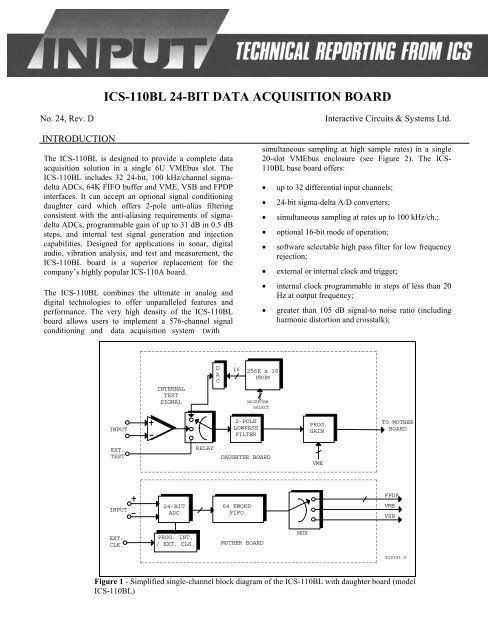
ICS-110BL 24-BIT DATA ACQUISITION BOARD - VoxTechnologies
ICS-110BL 24-BIT DATA ACQUISITION BOARD - VoxTechnologies
ICS-110BL 24-BIT DATA ACQUISITION BOARD - VoxTechnologies

Create successful ePaper yourself
Turn your PDF publications into a flip-book with our unique Google optimized e-Paper software.
<strong>ICS</strong>-<strong>110BL</strong> <strong>24</strong>-<strong>BIT</strong> <strong>DATA</strong> <strong>ACQUISITION</strong> <strong>BOARD</strong><br />
No. <strong>24</strong>, Rev. D<br />
INTRODUCTION<br />
The <strong>ICS</strong>-<strong>110BL</strong> is designed to provide a complete data<br />
acquisition solution in a single 6U VMEbus slot. The<br />
<strong>ICS</strong>-<strong>110BL</strong> includes 32 <strong>24</strong>-bit, 100 kHz/channel sigmadelta<br />
ADCs, 64K FIFO buffer and VME, VSB and FPDP<br />
interfaces. It can accept an optional signal conditioning<br />
daughter card which offers 2-pole anti-alias filtering<br />
consistent with the anti-aliasing requirements of sigmadelta<br />
ADCs, programmable gain of up to 31 dB in 0.5 dB<br />
steps, and internal test signal generation and injection<br />
capabilities. Designed for applications in sonar, digital<br />
audio, vibration analysis, and test and measurement, the<br />
<strong>ICS</strong>-<strong>110BL</strong> board is a superior replacement for the<br />
company’s highly popular <strong>ICS</strong>-110A board.<br />
The <strong>ICS</strong>-<strong>110BL</strong> combines the ultimate in analog and<br />
digital technologies to offer unparalleled features and<br />
performance. The very high density of the <strong>ICS</strong>-<strong>110BL</strong><br />
board allows users to implement a 576-channel signal<br />
conditioning and data acquisition system (with<br />
Interactive Circuits & Systems Ltd.<br />
simultaneous sampling at high sample rates) in a single<br />
20-slot VMEbus enclosure (see Figure 2). The <strong>ICS</strong>-<br />
<strong>110BL</strong> base board offers:<br />
• up to 32 differential input channels;<br />
• <strong>24</strong>-bit sigma-delta A/D converters;<br />
• simultaneous sampling at rates up to 100 kHz/ch.;<br />
• optional 16-bit mode of operation;<br />
• software selectable high pass filter for low frequency<br />
rejection;<br />
• external or internal clock and trigger;<br />
• internal clock programmable in steps of less than 20<br />
Hz at output frequency;<br />
• greater than 105 dB signal-to noise ratio (including<br />
harmonic distortion and crosstalk);<br />
INTERNAL<br />
TEST<br />
SIGNAL<br />
D<br />
A<br />
C<br />
16<br />
256K x 16<br />
PROM<br />
WAVEFORM<br />
SELECT<br />
INPUT<br />
2-POLE<br />
LOWPASS<br />
FILTER<br />
PROG.<br />
GAIN<br />
TO MOTHER<br />
<strong>BOARD</strong><br />
EXT.<br />
TEST<br />
RELAY<br />
DAUGHTER <strong>BOARD</strong><br />
VME<br />
FPDP<br />
INPUT<br />
<strong>24</strong>-<strong>BIT</strong><br />
ADC<br />
64 KWORD<br />
FIFO<br />
VME<br />
VSB<br />
EXT.<br />
CLK.<br />
PROG. INT.<br />
/ EXT. CLK.<br />
MOTHER <strong>BOARD</strong><br />
MUX<br />
K10391-0<br />
Figure 1 - Simplified single-channel block diagram of the <strong>ICS</strong>-<strong>110BL</strong> with daughter board (model<br />
<strong>ICS</strong>-<strong>110BL</strong>)
<strong>ICS</strong>-110B Sigma-Delta ADC Board<br />
• 64 Kword on-board storage;<br />
• VME, VSB and FPDP interfaces for ADC data;<br />
• front-panel sync bus for sample synchronization and<br />
Front Panel Data Port (FPDP) bussing of up to 32<br />
boards.<br />
The <strong>ICS</strong>-<strong>110BL</strong>, which contains the optional daughter<br />
card, features:<br />
• up to 32 differential inputs;<br />
• high input impedance;<br />
• 2-pole low pass anti-alias filters;<br />
• -95.0 dB to 31.5 dB programmable gain in steps of<br />
0.5 dB;<br />
• internal or external test signal injection to all 32<br />
channels by means of relays;<br />
• internal test signal stored in PROM (up to 8 16-bit<br />
signals of 32 K samples each).<br />
576 DIFF.<br />
ANALOG<br />
INPUTS<br />
{<br />
<strong>ICS</strong> -<br />
110B1<br />
<strong>ICS</strong> -<br />
110B1<br />
7220-<br />
ALU<br />
FPDP<br />
TO FOLLOWING<br />
SYSTEM<br />
SYNCHRONIZING<br />
SIGNAL BUS ENSURES<br />
SIMULTANEOUS<br />
SAMPLING OF ALL<br />
CHANNELS<br />
SYNC<br />
FPDP<br />
<strong>ICS</strong><br />
<strong>ICS</strong><br />
<strong>ICS</strong><br />
18 x <strong>ICS</strong>-110B1<br />
FOR SIGNAL<br />
CONDITIONING & <strong>24</strong>-<strong>BIT</strong><br />
<strong>DATA</strong> <strong>ACQUISITION</strong><br />
FPDP BUFFERING, AND<br />
TEST SIGNAL ADDITION<br />
K10391A1<br />
Figure 2 - A 576 channel signal conditioning and data acquisition system can now be included in a 20-slot VME<br />
enclosure using <strong>ICS</strong>-<strong>110BL</strong> boards<br />
Page 2
SPECIFICATIONS<br />
<strong>ICS</strong>-110B Sigma-Delta ADC Board<br />
<strong>ICS</strong>-<strong>110BL</strong> Mother Board<br />
No. of Diff. Analog Inputs: 8, 16 or 32<br />
Input Impedance:<br />
10 kOhm<br />
Full Scale Input:<br />
2.0 V pp differential*<br />
Max. Input Signal BW:<br />
40 kHz<br />
Input Sample Rate:<br />
128 X Output Rate for BW < 22 kHz<br />
64 X Output Rate for BW > 22 kHz<br />
Output Rate (Effective Sample Rate): Max. 100 kHz/Ch.<br />
Min. 2 kHz/Ch<br />
Internal Sample Clock:<br />
Programmable in steps of 20 Hz (at output frequency)<br />
Dynamic Range<br />
> 110 dB in 128x oversampling mode<br />
> 105 dB in 64x oversampling mode<br />
Total Harmonic Distortion:<br />
< -105 dB<br />
Crosstalk:<br />
< -105 dB<br />
On-Board Storage:<br />
64 K Words<br />
Output Word length:<br />
32 bits packed for 2 channels or <strong>24</strong> bits for<br />
1 channel on both VME or VSB<br />
<strong>24</strong> bits only on FPDP<br />
VMEbus Interface:<br />
A32/<strong>24</strong>/16 D32 BLT Slave<br />
Vectored Interrupts<br />
VSBbus Interface:<br />
A32 D32 BLT Slave<br />
Polled Interrupts<br />
FPDP Interface: Refer to <strong>ICS</strong> Input Technical Note No. 15<br />
Programmable Word Rate, up to 20Mwords/s<br />
Power:<br />
6.0 Amps @ +5 V<br />
0.42 Amps @ +12 V<br />
0.25 Amps @ -12 V<br />
Operating Temp:<br />
0 to +50 Deg. C<br />
Storage Temp:<br />
-40 to +85 Deg. C<br />
Humidity:<br />
#95% Rel. Humidity, non-condensing<br />
Board Size:<br />
6U VMEbus Standard<br />
<strong>ICS</strong>-<strong>110BL</strong> Daughter Card<br />
No. Of Diff Inputs: 8, 16 or 32<br />
Input Impedance:<br />
>1 M Ohm (with ±5 V max. input)<br />
>100 K Ohm (with ±25 V max. input)<br />
Max. Input Level:<br />
±3.75V differential standard option<br />
(Contact factory for other options)<br />
Lowpass Filter:<br />
2 - Pole Butterworth with a cut-off frequency of<br />
75 kHz for a flat response up to 40kHz<br />
(Contact Factory for Other Options)<br />
Gain:<br />
-95.0 dB to +31.5 dB in steps of 0.5 dB<br />
Internal Test Signal:<br />
8 16-bit preprogrammed waveforms<br />
in a 256K X 16 PROM<br />
Dynamic Range:<br />
>85 dB at 0 dB Gain and 2 Vpp Diff. Input<br />
Power:<br />
0.34 Amps @ +5 V<br />
0.29 Amps @ + 12 V<br />
0.20 Amps @ -12 V<br />
Environmental:<br />
Same as <strong>ICS</strong>-<strong>110BL</strong> Mother Board<br />
* 2.0Vpp on each wire of differential pair.<br />
Specifications are subject to change without notice<br />
Page 3
<strong>ICS</strong>-110B Sigma-Delta ADC Board<br />
GENERAL DESCRIPTION<br />
MOTHER <strong>BOARD</strong><br />
Figure 3 shows a simplified block diagram of the<br />
<strong>ICS</strong>-<strong>110BL</strong> baseboard. The board includes up to 32<br />
separate Sigma-Delta ADCs to simultaneously digitize all<br />
channels at rates up to 100 KHz/ch. All inputs are<br />
differential to suppress common mode noise. The serial<br />
output from each ADC is converted to a <strong>24</strong>-bit word<br />
before being stored in a FIFO for read-out.<br />
The <strong>ICS</strong>-<strong>110BL</strong> uses AKM’s AK5393 <strong>24</strong>-bit sigma-delta<br />
ADC converters. Each ADC converter samples the analog<br />
input signal at 64 or 128 times the output rate (Fo). For<br />
Fo < 50 kHz, 128 x oversampling mode is recommended.<br />
For Fo > 50 kHz only 64 x oversampling mode can be<br />
used. The sampling mode is set via the control register,<br />
which alters the decimation ratio of the digital filter. The<br />
maximum sample output frequency is 100 kHz. The<br />
AK5393 also includes a digital highpass filter after the<br />
decimator to remove low-frequency noise. The -3dB point<br />
is at 1.8 X Fs/48. In other words, the -3dB point of the<br />
highpass filter’s response is at 3.6 Hz for Fs=96 kHz. The<br />
high pass filter can be disabled using a bit in the control<br />
register. The standard group delay through the AK5393<br />
FIR low pass filters is 34/Fo (all filters are linear phase).<br />
The group delay can be reduced to 10/Fo if the minimum<br />
phase filter option is selected. All of the converter’s<br />
programmable features are available to the user.<br />
At the output, data is read as 32-bit words. Data from<br />
consecutive odd and even channels may be truncated to<br />
16-bit resolution and packed together to form a 32-bit<br />
word for faster read-out from the VMEbus or VSB. Data<br />
may also be read-out in unpacked format as <strong>24</strong>-bit words.<br />
The FPDP output, however, only supports unpacked<br />
format. A VMEbus or VSB interrupt can be generated at<br />
FIFO half-full to facilitate real-time operation.<br />
P5 FPDP<br />
SYNC*<br />
DVALID*<br />
<strong>DATA</strong><br />
STROBE<br />
SUSPEND*<br />
NRDY*<br />
<strong>24</strong><br />
SYNC WORD<br />
CH #0<br />
ADC<br />
FRONT-PANEL<br />
INTERFACE<br />
PROG.<br />
CLOCK<br />
CH #2<br />
.<br />
.<br />
.<br />
.<br />
ADC<br />
.<br />
.<br />
.<br />
.<br />
SERIAL TO<br />
PARALLEL<br />
AND<br />
16:1 MUX<br />
(EVEN)<br />
32K word<br />
FIFO<br />
W<br />
16<br />
CH #30<br />
ADC<br />
32<br />
CH #1<br />
ADC<br />
CH #3<br />
CH #31<br />
.<br />
.<br />
.<br />
.<br />
FSI<br />
ADC<br />
.<br />
.<br />
ADC<br />
CLK<br />
.<br />
.<br />
SERIAL TO<br />
PARALLEL<br />
AND<br />
16:1 MUX<br />
(ODD)<br />
SYNC WORD<br />
32K word<br />
FIFO<br />
W<br />
16<br />
VMEbus<br />
INTERFACE<br />
32 32<br />
FIFO<br />
HALF-FULL<br />
VMEbus<br />
INTERFACE<br />
32<br />
INTERRUPT<br />
32<br />
CLK<br />
FRAME_SYNC<br />
ACQUIRE_SYNC<br />
CONTROL<br />
LOGIC<br />
PROG.<br />
CLOCK<br />
VMEbus<br />
VSBbus<br />
EXT. ACQ.<br />
K10391A3.CFL<br />
P4 LOCAL BUS<br />
Figure 3 - <strong>ICS</strong>-<strong>110BL</strong> Mother Board Block Diagram<br />
VMEbus<br />
Page 4
. <strong>ICS</strong>-110B Sigma- Delta ADC Board<br />
The <strong>ICS</strong>-<strong>110BL</strong> can use either an external clock or the<br />
board’s internal clock as the sampling clock. The required<br />
clock frequency is 256 times the output data rate. The<br />
internal clock can be programmed to produce a sampling<br />
rate with excellent accuracy (usually to within 40ppm) by<br />
writing the appropriate clock frequency word to the<br />
board’s PROGRAM_CLOCK register. The minimum Fo<br />
is 2 kHz. The board includes a programmable decimator,<br />
which simply rejects output samples to reduce Fo by a<br />
factor of up to 16. Note, however, that the antialising<br />
characteristics of the sigma-delta converters are lost when<br />
this feature is selected. Hence, this mode should only be<br />
selected when using a Fo of less than 2kHz.<br />
The acquisition period can be controlled either from the<br />
VMEbus (through software control), or by applying an<br />
external signal conforming to differential TTL signal<br />
levels to the EXTERNAL_ACQUIRE input. A high level<br />
signal causes acquisition to occur, while a low level<br />
signal causes acquisition to stop. Acquisition is<br />
automatically synchronized so that a full frame of data is<br />
always written to the FIFO at the beginning or end of an<br />
acquisition cycle.<br />
The <strong>ICS</strong>-<strong>110BL</strong> includes a very powerful FPDP interface,<br />
which allows up to 32 <strong>ICS</strong>-<strong>110BL</strong> boards to be bussed.<br />
To synchronize multiple <strong>ICS</strong>-<strong>110BL</strong> boards, one board<br />
must be configured as “master” in order to supply<br />
synchronization signals to the other slave boards. These<br />
signals are available at the front-panel P4 local bus<br />
connector.<br />
DAUGHTER CARD<br />
The <strong>ICS</strong>-<strong>110BL</strong> base board includes a provision for a<br />
daughter card for signal conditioning. Figure 4 provides a<br />
simplified block diagram of the daughter card version<br />
(<strong>ICS</strong>-<strong>110BL</strong>), which includes the following:<br />
• A 2-pole low-pass filter with a fixed cut-off<br />
frequency of 75 kHz in order to ensure a flat<br />
passband response extending up to 40 kHz.<br />
Typically, no more than a 2-pole filter is<br />
required for anti-aliasing because of the high<br />
input sampling rate inherent in a sigma-delta<br />
ADC converter. An alternate filter cut-off<br />
frequency may be offered. Contact factory for<br />
details.<br />
all 32-signal conditioning and ADC stages. The<br />
test signal input is signal is single-ended. The<br />
internal test signal is generated from a<br />
preprogrammed PROM, which can hold as many<br />
as 8 waveforms up to 32K samples each. The<br />
PROM is operated in a loop address mode in<br />
order to generate a periodic signal. The standard<br />
option for test signals include: single-tone; dualtone;<br />
pseudo-noise; etc. A 16-bit filtered deltasigma<br />
DAC is used to produce an analog signal.<br />
The switching between the actual input signals,<br />
external test signal and internal test signal is<br />
done under software control.<br />
Other signal conditioning daughter cards are being<br />
planned for different applications. Please contact the<br />
factory for details.<br />
DETAILED DESCRIPTION<br />
DAUGHTER <strong>BOARD</strong><br />
Figure 4 shows a simplified block diagram of the signal<br />
conditioning daughter card for the <strong>ICS</strong>-<strong>110BL</strong> board. It<br />
includes, for each channel, a differential receiver, which<br />
offers high input impedance. A resistive divider stage is<br />
included at the input to allow an over voltage capability. The<br />
input impedance is dependent on the maximum voltage<br />
input requirement.<br />
The signal conditioning circuit also includes a 2-pole low<br />
pass filter with a fixed cut-off frequency and a gain stage<br />
which offers programmable gain from -95.0 dB to 31.5 dB<br />
in steps of 0.5 dB.<br />
For off-line test, an internal or an external test signal can be<br />
injected into the signal path following the differential<br />
receiver stage. The internal test signal is factory<br />
programmed in to a 256K x 16 EPROM. The user can select<br />
one of any 8 pre-stored signals. A 16-bit delta-sigma DAC is<br />
used for digital-to-analog conversion. The typical dynamic<br />
range is around 90 dB. Note that high-reliability electromechanical<br />
relays are used to switch between<br />
internal/external test signals or actual signals. All channels<br />
receive the same test signals.<br />
• A programmable attenuation/gain stage which<br />
offers -95.0 dB to +31.5 dB attenuation/gain in<br />
steps of 0.5 dB.<br />
• An internal or external test signal injection<br />
capability that allows injection of a test signal to<br />
Page 5
<strong>ICS</strong>-110B Sigma-Delta ADC Board<br />
EPROM<br />
WAVE<br />
TABLE<br />
16<br />
DAC<br />
EXT.<br />
TEST<br />
SIGNAL<br />
RELAY<br />
FROM<br />
<strong>ICS</strong>-110B<br />
INPUT<br />
CONNECTOR<br />
RI<br />
RI<br />
+<br />
-<br />
INT./EXT.<br />
TEST<br />
DIFF. RELAY<br />
RECEIVER<br />
R2 R2 2-POLE LOWPASS FILTER<br />
GAIN<br />
8<br />
VME<br />
TO<br />
MOTHER<br />
<strong>BOARD</strong><br />
INPUTS<br />
K10391-2<br />
Figure 4 - Signal Conditioning Daughter Card (Single Channel Shown)<br />
MOTHER <strong>BOARD</strong><br />
Sigma-Delta Analog Conversion<br />
The operation of a Sigma-Delta ADC differs significantly<br />
from traditional ADCs. A simple 1-bit analog-to-digital<br />
conversion is performed at a very high rate. The total<br />
quantization noise energy remains constant, but by<br />
spreading it over a wider spectrum, the amount in the<br />
frequency band of interest is reduced. The noise in the<br />
passband is further reduced by filtering (noise shaping). The<br />
oversampled signal is then lowpass filtered to remove the<br />
out-of-band quantization noise. This is achieved using two<br />
digital filters: a decimating comb filter and an FIR low-pass<br />
filter/decimator. The resultant output spectrum is equivalent<br />
to a traditional ADC.<br />
The AK5393 uses a 7th order tri-level delta-sigma<br />
modulator to sample the analog input signal at either 128 or<br />
64 times the output sample rate of the device. The result of<br />
such high rate sampling of the input signal is that the<br />
Nyquist frequency is moved to at least 6 octaves (for 64<br />
times oversampling) or 7 octaves (for 128 times<br />
oversampling) away from the highest signal frequency. The<br />
anti-aliasing requirement is, therefore, drastically reduced.<br />
Since the input differential amplifier for each channel of the<br />
<strong>ICS</strong>-<strong>110BL</strong> board has a finite bandwidth, no more than a 2-<br />
pole filter is required for anti-aliasing. The signal<br />
conditioning daughter card of the <strong>ICS</strong>-<strong>110BL</strong> board<br />
includes a filter of this type.<br />
10K<br />
+1V<br />
-1V<br />
+<br />
10K<br />
-<br />
+<br />
- ve<br />
INPUT SIGNAL<br />
+ 1.25v<br />
TO ADC INPUT<br />
+1V<br />
-1V<br />
-<br />
10K<br />
+<br />
-<br />
+ ve<br />
10K<br />
K10166-2<br />
Figure 5 - <strong>ICS</strong>-<strong>110BL</strong> Analog Input Configuration<br />
Page 6
. <strong>ICS</strong>-110B Sigma- Delta ADC Board<br />
Input Section<br />
The <strong>ICS</strong>-<strong>110BL</strong> board accepts true differential input signals;<br />
peak amplitudes of ± 1.0V on each input, as shown in Figure<br />
5, produce a full-scale output. The input impedance is 10K<br />
ohm. The maximum input signal bandwidth is 40 kHz.<br />
For best performance, differential input signals are<br />
recommended. If, however, single-ended inputs must be<br />
used, the -ve input terminals can be tied to a common analog<br />
ground, preferably the ground of the source. The input<br />
signal is applied to the +ve terminal. The full-scale swing of<br />
the input signal should not exceed ± 1.0V. Thus, for single<br />
ended input, there is a 6 dB loss in dynamic range.<br />
Dynamic Range<br />
The <strong>ICS</strong>-<strong>110BL</strong> typically offers 110 dB S/N ratios in the<br />
128 times oversampling mode. The S/N ratio is<br />
approximately 105 dB in the 64 times oversampling mode.<br />
The total harmonic distortion is typically -105 dB. A typical<br />
10<strong>24</strong>-point FFT plot of the ADC output is shown in Figure<br />
6(a). The input is a synthesized single tone (differential) and<br />
the output rate is 100 kHz/channel. The crosstalk<br />
performance of a typical channel (input shorted) while all<br />
other channels are driven by a 20 kHz tone is illustrated in<br />
Figure 6(b). Note that all spurious components lie below -<br />
110 dB with respect to the ADC full-scale output.<br />
The <strong>ICS</strong>-<strong>110BL</strong> offers excellent gain and phase matching<br />
across channels. Since the Sigma-Delta converters employ<br />
minimal analog technologies, such performance is expected.<br />
In the design of the <strong>ICS</strong>-<strong>110BL</strong> board, extreme care has<br />
been<br />
Taken in the generation of sampling clocks in order to<br />
assure precise simultaneous sampling on every card, and<br />
across cards in a multi-board system.<br />
The frequency response is flat over the entire signal<br />
bandwidth (45% of the output rate).<br />
Sampling Clock<br />
The <strong>ICS</strong>-<strong>110BL</strong> board can be configured (by programming<br />
the control register) for internal or external sampling. The<br />
external CLOCK input is TTL differential. A single-ended<br />
TTL clock signal can also be used provided that the high<br />
logic level is above 3.5 volts. This CLOCK input frequency<br />
must be 256 times the desired output.<br />
As mentioned above, the sampling clock can also be sourced<br />
from an internal programmable clock oscillator, which has a<br />
resolution of less than 20 Hz at the sample output frequency.<br />
The internal clock (after conversion to differential TTL<br />
signals) is available at the P4 front-panel connector pins in<br />
order to supply clock signals to other <strong>ICS</strong>-110B boards for<br />
synchronous operation. The board generating the clock<br />
signal (master board) requires appropriate jumper settings in<br />
order to route the clock signals back to the P4 connector.<br />
All slave <strong>ICS</strong>-<strong>110BL</strong> boards must be configured for external<br />
clock. Thus all boards including the master see identical<br />
propagation delays for the clock signal, regardless of<br />
whether it is generated by an <strong>ICS</strong>-<strong>110BL</strong> board or applied<br />
from an external source. The maximum clock frequency is<br />
25.6 MHz and the minimum clock frequency is 512 kHz.<br />
Output Decimation<br />
The output rate can be reduced using decimation. At the<br />
output, samples are automatically discarded, which has the<br />
effect of lowering the effective sampling rate. The<br />
decimation factor can be as high as 16.<br />
The user is cautioned that decimating the output requires<br />
anti-aliasing (similar to using a conventional ADC) in order<br />
to bandlimit the input signal to the Nyquist frequency, which<br />
is equal to half the final output rate. Thus, output<br />
decimation is only recommended for reducing the output<br />
rate below 2 kHz.<br />
Page 7
<strong>ICS</strong>-110B Sigma-Delta ADC Board<br />
0<br />
-20<br />
-40<br />
-60<br />
Amplitude [dB]<br />
-80<br />
-100<br />
-120<br />
-140<br />
-160<br />
100 200 300 400 500 600 700 800 900 1000<br />
Frequency [bin]<br />
Figure 6(a) - 2048-point FFT in <strong>24</strong>-bit mode at 100 kHz<br />
0<br />
-20<br />
-40<br />
-60<br />
Amplitude [dB]<br />
-80<br />
-100<br />
-120<br />
-140<br />
-160<br />
100 200 300 400 500 600 700 800 900 1000<br />
Frequency [bin]<br />
Figure 6(b) - Crosstalk Performance with 20 kHz Tone on all Other Channels<br />
Page 8
. <strong>ICS</strong>-110B Sigma- Delta ADC Board<br />
<strong>DATA</strong>_CLOCK<br />
FPDP_<strong>DATA</strong><br />
0 1 2 30 31 32 33 34 62 63<br />
BUS_IDLE MASTER DRIVES BUS SLAVE WITH <strong>BOARD</strong>_ADDRESS=1 DRIVES BUS BUS_IDLE<br />
<strong>DATA</strong>_STROBE<br />
/SYNC<br />
Figure 7 - FPDP Timing with Multiple Boards<br />
MASTER ALWAYS DRIVES <strong>DATA</strong>_STROBE & /SYNC<br />
K10187-<br />
Acquisition Trigger<br />
The triggering of acquisition can be done either internally,<br />
by writing to the control register, or externally, by applying<br />
a signal to the EXTERNAL_ACQUIRE input. In either<br />
case, the effect is to start and stop acquisition by inhibiting<br />
FIFO writes; the ADCs are always converting data. The<br />
operation is frame-oriented: acquisition can only be started<br />
at the beginning of a frame and stopped at the end of a<br />
frame; a frame is defined as a set of sampled data for all<br />
selected channels for one sample instant. The number of<br />
channels included in the frame is programmable, but always<br />
starts from channel 1 and runs consecutively up to the<br />
number of channels selected. Only even numbers of<br />
channels may be selected.<br />
For external control of acquisition start/stop, the differential<br />
EXTERNAL_ACQUIRE input must be used. A TTL high<br />
level starts acquisition and the acquisition stops when the<br />
signal is dropped to a TTL low level. Bringing the signal<br />
back to a TTL high level can restart the acquisition. Here<br />
again, a single-ended TTL signal can be used provided the<br />
high logic level is above 3.5 volts.<br />
SYNC Word<br />
When reading data from the 32-bit VMEbus or VSB<br />
interface, a user-programmable 32-bit sync word can be<br />
used to maintain synchronization. This optional<br />
SYNC_WORD<br />
is automatically written to the ADC_<strong>DATA</strong> FIFO at the<br />
beginning of every frame. The SYNC_WORD option is not<br />
available on the front panel data port.<br />
Front Panel Interface<br />
The <strong>ICS</strong>-<strong>110BL</strong> includes a Front Panel Data Port (FPDP)<br />
for high-speed data transfer. The FPDP protocol for data<br />
transfer is supported by all <strong>ICS</strong> products, including the <strong>ICS</strong>-<br />
2200 DSP board, the <strong>ICS</strong>-7220 General Purpose I/O board,<br />
and the <strong>ICS</strong>-115 Analog Output board. An 80-pin<br />
connector (KEL 8831-080-170L) is provided for the FPDP.<br />
Refer to INPUT Technical Note No.15 for more details.<br />
The <strong>ICS</strong>-<strong>110BL</strong> FPDP may be bussed between multiple<br />
<strong>ICS</strong>-<strong>110BL</strong> boards for systems requiring more than 32<br />
channels of analog input. The first board of a cluster must<br />
be configured as the master, by means of wire links on the<br />
board. The master generates the FPDP Strobe, Data Valid<br />
and Sync signals and terminates various bus signals. It<br />
also generates signals on the P4 local bus, which control<br />
the timing for the slave boards so that each board drives<br />
its data onto the bus in the correct time period. This<br />
feature, combined with the multiple board<br />
synchronization capability of the <strong>ICS</strong>-<strong>110BL</strong> described<br />
elsewhere in this note, allows the user to construct large<br />
data acquisition systems of up to 1,0<strong>24</strong> channels with<br />
simultaneous sampling across all channels and a single<br />
FPDP cable passing data to one or more FPDP receive<br />
interfaces.<br />
Figure 7 illustrates the timing relationship of the FPDP data<br />
and control signals for a 2 board 64-channel system. The<br />
FPDP Data Strobe (clock) rate is software programmable,<br />
with a maximum frequency of 20 MHz. Two types of Data<br />
Strobe signal are available: the TTL level STROB and the<br />
positive-logic ECL differential clocks (PSTROBE+ &<br />
PSTROBE-). The latter signals support longer cable lengths<br />
and higher speed operation, and provide better noise<br />
immunity. The <strong>ICS</strong>-<strong>110BL</strong> supports only the unpacked <strong>24</strong>-<br />
bit data width on the FPDP port.<br />
Page 9
<strong>ICS</strong>-110B Sigma-Delta ADC Board<br />
The Front Panel Data Port operates using two FIFO<br />
memories in a swing buffer configuration, as shown in<br />
Figure 8. During one frame, data is converted and written to<br />
one FIFO memory, while data is being read from the other<br />
over the FPDP. At the end of the frame, the two banks<br />
switch. Before any new ADC data is written to the swapped<br />
FIFO memory, it is automatically reset to ensure channel<br />
synchronization. In the unlikely event that the<br />
synchronization is lost, the scheme ensures that it is<br />
recovered in the next frame.<br />
By programming the FPDP_BLOCK_COUNT register, the<br />
user can set the bank switch to occur after storing a userprogrammable<br />
number of frames.<br />
VMEbus Interface<br />
The <strong>ICS</strong>-<strong>110BL</strong> is supported by a Slave A32/D32 VMEbus<br />
interface. The VMEbus interface supports D32 block<br />
transfers and vectored interrupts. Data rates up to 32<br />
MBytes/sec are achievable.<br />
Although data is always accessed using 32-bit data transfers,<br />
channel data can be organized as two channels per transfer<br />
(packed format) or one channel per transfer (unpacked<br />
format). In packed format, the data is truncated to 16 bits<br />
and ordered so that channel N is in the upper 16 bits, and<br />
channel N+1 is in the lower 16 bits of the 32-bit data word.<br />
In unpacked format, the channel data is located in the upper<br />
<strong>24</strong> bits of the 32-bit data word; the lower 8 bits are forced to<br />
zero.<br />
VSB Interface<br />
The <strong>ICS</strong>-<strong>110BL</strong> also includes a Slave A32/D32 VSB<br />
interface. The VSB interface supports block transfers, as<br />
well as polled interrupts. Data rates up to 40 MBytes/sec are<br />
achievable. Data organization is as discussed in the<br />
VMEbus Interface section.<br />
Multiple-Board Synchronization<br />
An important design feature of the <strong>ICS</strong>-<strong>110BL</strong> card is its<br />
ability to be integrated into a multi-board system in perfect<br />
synchronism using no additional hardware and no additional<br />
design effort. This section discusses in some detail the P4<br />
Local Bus signals used to achieve synchronism in a multiboard<br />
system. The interface requires only the bussing of the<br />
master <strong>ICS</strong>-<strong>110BL</strong> P4 Local Bus connector to one or more<br />
slave cards, and the initialization of a few registers on the<br />
master.<br />
To ensure sampling synchronization from board to board in<br />
a multiple board configuration, three synchronization signals<br />
are driven by the master <strong>ICS</strong>-<strong>110BL</strong> and decoded by all<br />
boards across the P4 Local Bus connector. To keep<br />
sampling skew to a minimum, all SYNC signals are<br />
generated and then received locally by the master, so that the<br />
master sees the same gate delays and decoding logic as seen<br />
by the slave cards. In effect, the master is its own slave.<br />
STROBE (TTL or PECL DIFF.)<br />
<strong>DATA</strong> VALID<br />
SYNC<br />
SUSPEND<br />
<strong>DATA</strong><br />
16<br />
FPDP<br />
I/F<br />
CH#1<br />
ADC<br />
CH#32<br />
ADC<br />
SERIAL TO<br />
PARALLEL<br />
AND<br />
MUX<br />
FIFO<br />
FIFO<br />
K10184-5<br />
Figure 8 - <strong>ICS</strong>-<strong>110BL</strong> FPDP Configuration<br />
Page 10
. <strong>ICS</strong>-110B Sigma- Delta ADC Board<br />
CLOCK<br />
FRAME_SYNC<br />
LOCAL ADC CLOCK<br />
SYNC UP<br />
SAMPLING INSTANTS<br />
K10184A2<br />
Figure 9 - Master/Slave CLOCK Phase Synchronization<br />
FRAME_SYNC<br />
The FRAME_SYNC signal is used to synchronize all<br />
boards with respect to the sampling clock. This signal is<br />
received.<br />
By each slave board and used to re-synchronize the<br />
converters at the next rising edge of the oversampling clock,<br />
as shown in Figure 9<br />
ACQUIRE_SYNC<br />
The <strong>ICS</strong>-<strong>110BL</strong> is capable of decimating the Sigma-Delta<br />
output by a user-defined number of frames. The<br />
ACQUIRE_SYNC signal simply ensures that both the<br />
master and its slaves decimate the same frames by informing<br />
the slaves who converted data frame is to be stored to the<br />
ADC_<strong>DATA</strong> FIFO. Decimated frames are simply rejected<br />
and not written to the ADC_<strong>DATA</strong> FIFO.<br />
Memory Map<br />
The <strong>ICS</strong>-<strong>110BL</strong> memory map is shown in Figures 10, 11<br />
and 12. Figure 10 shows a summary of the map, while<br />
Figures 11 and 12 show the bit allocation within registers.<br />
The control register allows the user to configure the<br />
following operating parameters:<br />
• Acquisition start and stop control<br />
• Master/slave (multiple board) selection<br />
• Acquisition source (internal/external)<br />
• Output mode (VMEbus, VSB, FPDP)<br />
• Sync word enable/disable<br />
• Clock source (internal/external)<br />
• VSB interrupt enable/disable<br />
• VMEbus interrupt enable/disable<br />
Register Descriptions<br />
The NUM_CHANS register must be programmed to specify<br />
the number of channels to be used on the board. The<br />
NUM_CHANS_FPDP register allows the user to select the<br />
total number of channels when using the FPDP for output<br />
with multiple <strong>ICS</strong>-<strong>110BL</strong> boards; it only needs to be<br />
programmed on the master board. The number of channels<br />
in either case must be an even number, and, in a multiple<br />
board configuration, all boards except the last must be 32-<br />
channel boards and must have a full complement of<br />
channels selected.<br />
For example, an 80-channel system would consist of three<br />
boards defined as follows:<br />
Master:<br />
Middle Slave:<br />
End Slave:<br />
NUM_CHANS=31 (32 channels)<br />
NUM_CHANS_FPDP=79 (80 channels)<br />
NUM_CHANS=31 (32 channels)<br />
NUM_CHANS=15 (16 channels)<br />
The maximum number of channels in a multiple board<br />
system when using the front panel data port is limited to<br />
1,0<strong>24</strong>, i.e. 32 boards (NUM_CHANS_FPDP=1023).<br />
The DECIMATION register allows the user to specify the<br />
decimation factor in the range 1 to 16. The FPDP<br />
ADDRESS register specifies the board address in a multiple<br />
board system when using FPDP.<br />
Page 11
<strong>ICS</strong>-110B Sigma-Delta ADC Board<br />
VMEbus<br />
D31<br />
D15<br />
D0<br />
BASE + 0x0<br />
ADC <strong>DATA</strong><br />
STATUS/RESET<br />
CONTROL<br />
INT. VECTOR<br />
NUM CHANS<br />
DECIMATION<br />
ADC CONFIGURATION<br />
CALIBRATION<br />
FPDP ADDRESS<br />
NUM CHANS FPDP<br />
FPDP BLOCK COUNT<br />
VSB BASE ADDRESS<br />
VSB SPACE CODE<br />
SYNC WORD<br />
CLOCK FREQUENCY<br />
BASE + 0xFE00<br />
BASE + 0xFE02<br />
BASE + 0xFE04<br />
BASE + 0xFE06<br />
BASE + 0xFE08<br />
BASE + 0xFE0A<br />
BASE + 0xFE0C<br />
BASE + 0xFE0E<br />
BASE + 0xFE10<br />
BASE + 0xFE12<br />
BASE + 0xFE14<br />
BASE + 0xFE16<br />
BASE + 0xFE18<br />
BASE + 0xFE1C<br />
D31<br />
VSBbus<br />
ADC_<strong>DATA</strong><br />
D0<br />
BASE + 0x0<br />
VSB STATUS<br />
BASE + 0x8000<br />
INTERRUPT ENABLE<br />
BASE + 0xC000<br />
K10373-0<br />
Figure 10 - <strong>ICS</strong>-<strong>110BL</strong> Memory Map<br />
Page 12
. <strong>ICS</strong>-110B Sigma- Delta ADC Board<br />
D8<br />
D7<br />
D3 D2 D1 D0<br />
<strong>BOARD</strong><br />
RESET<br />
FIFO<br />
RESET<br />
ACQUIRE<br />
ENABLED<br />
/FIFO<br />
FULL<br />
/FIFO<br />
HALF-<br />
FULL<br />
/FIFO<br />
EMPTY<br />
BASE + 0xFE00 READ/WRITE STATUS/RESET<br />
D15 D14 D8 D7 D6 D5 D4 D3 D2 D1 D0<br />
VME_INT<br />
ENABLE<br />
VSB_INT<br />
ENABLE<br />
OVER-<br />
SAMPLING<br />
RATIO<br />
CLOCK<br />
SEL<br />
SYNC<br />
ENABLE<br />
OUTPUT MODE<br />
ACQUIRE<br />
SOURCE<br />
MASTER<br />
ACQUIRE<br />
BASE + 0xFE02 READ/WRITE CONTROL<br />
D7 D6 D5 D4 D3 D2 D1 D0<br />
INTERRUPT_VECTOR<br />
BASE + 0xFE04 READ/WRITE INTERRUPT_VECTOR<br />
D3 D2 D1 D0<br />
NUM_CHANNELS<br />
BASE + 0xFE06 WRITE ONLY NUM_CHANNELS<br />
D4<br />
D3 D2 D1 D0<br />
DECIMATION<br />
BASE + 0xFE08 WRITE ONLY DECIMATION<br />
D7 D6 D5<br />
D4<br />
D3 D2 D1 D0<br />
CHIP<br />
SEL<br />
ADC_CONFIGURATION<br />
BASE + 0xFE0A WRITE ONLY ADC_CONFIGURATION<br />
D7 D6 D2 D1 D0<br />
CLOCK<br />
SEL<br />
CAL<br />
ENABLE<br />
BASE + 0xFE0C READ/WRITE ADC_CALIBRATION<br />
CAL<br />
SEL<br />
2<br />
CAL<br />
SEL<br />
1<br />
CAL<br />
SEL<br />
0<br />
D4 D3 D2 D1 D0<br />
FPDP_ADDRESS<br />
BASE + FE0E WRITE ONLY FPDP_ADDRESS<br />
D9<br />
D8<br />
D7 D6 D5 D4 D3 D2 D1 D0<br />
NUM_CHANNELS_FPDP<br />
BASE + FE10 WRITE ONLY NUM_CHANNELS_FPDP<br />
K10373A1<br />
Figure 11 - <strong>ICS</strong>-<strong>110BL</strong> Register Description<br />
Page 13
<strong>ICS</strong>-110B Sigma-Delta ADC Board<br />
D7 D6 D5 D4 D3 D2 D1 D0<br />
FPDP_BLOCK_COUNT<br />
BASE + 0xFE12 WRITE ONLY FPDP_BLOCK_COUNT<br />
D15<br />
D14<br />
D7 D6 D5 D4 D3 D2 D1 D0<br />
VSB_BASE_ADDR<br />
BASE + 0xFE14 WRITE ONLY VSB_BASE_ADDR<br />
D1<br />
D0<br />
VSB_SPACE_CODE<br />
BASE + 0xFE16 WRITE ONLY VSB_SPACE_CODE<br />
D31<br />
D30<br />
D7 D6 D5 D4 D3 D2 D1 D0<br />
SYNC_WORD<br />
BASE + 0xFE18 WRITE ONLY SYNC_WORD<br />
D23 D21 D20 D19 D4 D3 D2 D1 D0<br />
DEST.<br />
CLOCK_FREQUENCY<br />
BASE + 0xFE1C WRITE ONLY CLOCK_FREQUENCY<br />
D31 D30 D29<br />
D28 D26 D25 D<strong>24</strong><br />
VSB<br />
INT.<br />
/FIFO<br />
FULL<br />
/FIFO<br />
HALF-<br />
FULL<br />
/FIFO<br />
EMPTY<br />
GLOBAL ADDRESS<br />
BASE + 0x8000 READ ONLY VSB_STATUS<br />
K10373A2<br />
Figure 12 - <strong>ICS</strong>-<strong>110BL</strong> Register Descriptions (cont’d)<br />
Page 14
. <strong>ICS</strong>-110B Sigma- Delta ADC Board<br />
SOFTWARE DEVICE DRIVERS<br />
A comprehensive software device driver for the VxWorks<br />
real-time operating system supports the <strong>ICS</strong>-<strong>110BL</strong>. The<br />
driver includes the following elements:<br />
• A device driver conforming to the VxWorks model,<br />
including support for Open, Close, Read, Write and<br />
IOCTL functions, and device initialization and<br />
attachment.<br />
• A comprehensive library of high-level functions,<br />
which may be included with the application<br />
programmer’s code. They provide control of all<br />
aspects of the <strong>ICS</strong>-<strong>110BL</strong>. Programmers are advised<br />
to use the library in preference to direct use of the<br />
device driver interface, since this will reduce the<br />
need to understand the details of board operation and<br />
will speed up integration.<br />
• Driver and library source code. For users who wish<br />
to port the driver to their own operating system,<br />
complete ‘C’ language source code is provided.<br />
The following are examples of some of the library<br />
routines. Each function carries a list of parameters that are<br />
not described here:<br />
ics110blSampleRateSet()<br />
ics110blVmeInterruptWait()<br />
ics110blDeviceReset()<br />
ics110blMasterSet()<br />
ics110blAcqSrcSet()<br />
int ics110blOutputModeSet()<br />
ics110blOversamplingSet()<br />
ics110blDecimationSet()<br />
ics110blIntVectorSet()<br />
ics110blVsbBaseAddressSet()<br />
ics110blStatusRead()<br />
ics110blFifoRead()<br />
ics110blSampleRateSet()<br />
ics110blProgramAdc()<br />
ics110blCalibrateAdc()<br />
ics110blGainSet()<br />
ics110blAcquireSet()<br />
Sets the sampling frequency.<br />
Waits for interrupt or timeout to occur<br />
Resets <strong>ICS</strong>-<strong>110BL</strong> to initial conditions<br />
Sets board as sampling master (for multiple board configurations)<br />
Sets acquisition trigger as internal or external<br />
Sets the output path as VMEbus, VSB or FPDP<br />
Sets the converter oversampling ratio<br />
Set decimation ratio<br />
Load VMEbus interrupt vector<br />
Load VSB base address<br />
Read board status<br />
Read sample data<br />
Set frequency of onboard sampling clock<br />
Set converter characteristics such as software initiated calibration, FIR filter coefficients<br />
Calibrate <strong>ICS</strong>-<strong>110BL</strong> converters<br />
Set signal conditioner gain<br />
Start conversion<br />
INPUT is published by <strong>ICS</strong> Ltd. and is available free of charge. Your input is welcome; please call or write to <strong>ICS</strong>.