H1 FTT L1 deliverables and milestones
H1 FTT L1 deliverables and milestones
H1 FTT L1 deliverables and milestones

Create successful ePaper yourself
Turn your PDF publications into a flip-book with our unique Google optimized e-Paper software.
<strong>H1</strong> <strong>FTT</strong> <strong>L1</strong> <strong>deliverables</strong> <strong>and</strong> <strong>milestones</strong><br />
D P C Sankey - RAL<br />
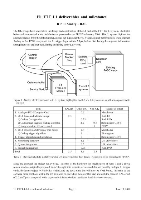
The UK groups have undertaken the design <strong>and</strong> construction of the <strong>L1</strong> part of the <strong>FTT</strong>, the <strong>L1</strong> system, illustrated<br />
below <strong>and</strong> summarised in the table below as presented to the PPESP in January 2000. This <strong>L1</strong> system digitises the<br />
analogue signals from the drift chamber, carries out in parallel the “Q-t” analysis <strong>and</strong> performs local track segment<br />
finding in fast FPGA arrays <strong>and</strong> the <strong>L1</strong> trigger logic within 2.3 µs, before distributing the segment information<br />
appropriately for the later track linking <strong>and</strong> fitting in the L2 system.<br />
Central<br />
Trigger<br />
Central<br />
Tracker<br />
Daq<br />
Existing<br />
DCrφ<br />
card<br />
Daughter<br />
card<br />
Existing<br />
FADC cards<br />
Crate controller<br />
Service Module<br />
<strong>L1</strong><br />
Front-end<br />
Module<br />
L2 <strong>and</strong> L3<br />
systems<br />
Figure 1 - Sketch of <strong>FTT</strong> hardware with <strong>L1</strong> system highlighted <strong>and</strong> L2 <strong>and</strong> L3 systems in solid lines as proposed to<br />
PPESP.<br />
Item RAL ID Other UK Non-UK Source of Effort<br />
1. Analogue DCrφ Daughter Card 0.6 Manchester<br />
2. a) <strong>L1</strong> Front-end Module design 2.5 RAL ID<br />
b) Coding Q-t algorithm 0.25 RAL PPD<br />
c) Coding track segment finding algorithm 2.2 0.3 Birmingham/DESY<br />
d) Integration into <strong>H1</strong> <strong>and</strong> control 1 DESY<br />
3. a) <strong>L1</strong> service module/trigger card design 0.8 Manchester<br />
b) Coding trigger algorithm 1 Birmingham<br />
4. Trigger algorithms <strong>and</strong> simulation 1 1 Birmingham/DESY<br />
5. Monitoring software 1.5 UK universities<br />
6. System integration 0.5 UK universities<br />
7. Project management 0.75 RAL PPD<br />
Total 2.5 8.6 2.3<br />
Table 1 - Revised schedule in staff years for UK involvement in Fast Track Trigger project as presented to PPESP.<br />
Since the proposal the project has evolved. In terms of the hardware the specification of items 1 <strong>and</strong> 2 above<br />
remain much as originally proposed, item 3 has split into separate service modules <strong>and</strong> possibly multiple <strong>L1</strong> trigger<br />
cards, the latter subject to feasibility studies, <strong>and</strong> the back-plane bus will now be VME based. In terms of the<br />
software more emphasis within the UK is placed on providing the algorithm 2(c) <strong>and</strong> with the reduced RAL effort<br />
of 2.5 staff years compared to the requested 4 it is not obvious that items 5 <strong>and</strong> 6 are now covered.<br />
<strong>H1</strong> <strong>FTT</strong> <strong>L1</strong> <strong>deliverables</strong> <strong>and</strong> <strong>milestones</strong> Page 1 June 13, 2000
Hardware Components<br />
DCrφ Daughter Card<br />
Hardware Description<br />
Amplifies the signals from 6 of the 8 wires coming out the front panel DIN connector on an existing F1001<br />
ADC card <strong>and</strong> passes these to the FEM. Also passes through the signals for 6 of the 8 wires to the existing<br />
DCrφ cards. Unfortunately there are at least two different sets of 6 wires required for the FEM <strong>and</strong> no doubt<br />
different sets for the DCrφ cards so probably at least 4 variants of this card need to be produced.<br />
Interfaces<br />
DIN connector into existing F1001 ADC card<br />
DIN socket for existing DCrφ card<br />
Socket for cable to FEM<br />
Responsibility<br />
Manchester<br />
Time scales<br />
Table 2 - DCrφ daughter card time scales<br />
Task Delivery date<br />
Design before 09/00<br />
Production before 11/00<br />
Installation before 03/01<br />
Concerns<br />
How many variants required<br />
Power load on ADC crate - some crates are already on the limit with the existing DCrφ cards.<br />
Front-End Module<br />
Hardware Description<br />
Takes signals from 5 groups (cells) of 6 wires (actually from both ends of 3 wires). Digitises these signals at<br />
80 MHz (to match the later synchronisation frequency) to give fast timing information for local segment<br />
finding, with slower z determination by charge division.<br />
Exchange information between neighbouring cells (including between adjacent modules in logical ring) to<br />
allow segment finding in cases where tracks cross cell boundaries.<br />
Provide sufficient FPGA resource to allow at a minimum the Q-t digitisation <strong>and</strong> the local segment finding<br />
<strong>and</strong> refinement algorithm after <strong>L1</strong>KEEP <strong>and</strong> ideally also fast local segment finding in time to contribute to an<br />
<strong>L1</strong> decision.<br />
Pass refined segments to L2 system after <strong>L1</strong>KEEP, also have functionality to pass fast segment information<br />
to <strong>L1</strong> trigger modules.<br />
Interfaces<br />
Input for cable from daughter card above - probably on front panel<br />
Output for cable to L2 system - probably 14526-EZHB-200-0QC type cable <strong>and</strong> 10226-1210VE board<br />
connectors on front panel as suggested by SCS - but possibly by connection through back-plane<br />
Interchange for 80 MHz information between adjacent modules in ring for segment finding via back-plane<br />
Output of fast segment information (or κφ histogram) to <strong>L1</strong> trigger modules via back-plane<br />
<strong>H1</strong> <strong>FTT</strong> <strong>L1</strong> <strong>deliverables</strong> <strong>and</strong> <strong>milestones</strong> Page 2 June 13, 2000
Minimal VME interface for downloading algorithm to FPGA, diagnostics <strong>and</strong> monitoring<br />
Access to trigger signals<br />
Responsibility<br />
RAL as detailed below<br />
Task Staff months Name<br />
1. Analogue design 2 AB & DL<br />
2. Digital design 4 AB & DL<br />
3. PCB layout 6 BC<br />
4. Debug 4 AB & DL & Technician<br />
5. Firmware 4 DL<br />
6. Production 4 Technician<br />
7. Commissioning <strong>and</strong> installation 2 AB & DL<br />
8. Control software 4 Real-time Systems Group<br />
Total 30<br />
Table 3 - Detailed breakdown of effort from RAL Instrumentation Department for construction of the <strong>H1</strong> Fast Track<br />
Trigger <strong>L1</strong> Front-end Module. The key for names is AB - Adam Baird, DL - transfer from Daresbury (tbc) <strong>and</strong><br />
BC - Brian Claxton.<br />
Time scales<br />
Task Start End<br />
Preliminary design report 01/00 03/00<br />
First design 03/00 06/00<br />
Board layout 06/00 12/00<br />
Prototype manufacture 12/00 01/01<br />
Debug / testing prototype in isolation 01/01 03/01<br />
Installation of prototype at <strong>H1</strong> 03/01<br />
Redesign <strong>and</strong> layout 04/01 06/01<br />
Main production 06/01 12/01<br />
Table 4 - FEM time scales<br />
Concerns<br />
Delay<br />
Not compatible with L2 prototypes available in October 2000<br />
Controller Module<br />
Hardware Description<br />
Interfaces<br />
Interface to <strong>H1</strong> trigger signals <strong>and</strong> broadcast to FEMs<br />
Interface to <strong>H1</strong> Daq for monitoring <strong>and</strong> download of FPGA code<br />
Responsibility<br />
Manchester<br />
<strong>H1</strong> <strong>FTT</strong> <strong>L1</strong> <strong>deliverables</strong> <strong>and</strong> <strong>milestones</strong> Page 3 June 13, 2000
Time scales<br />
Concerns<br />
<strong>L1</strong> Trigger Module<br />
Hardware Description<br />
Interfaces<br />
Trigger signals to <strong>H1</strong> <strong>L1</strong> Central Trigger logic<br />
Connections from FEMs<br />
Responsibility<br />
Manchester/Birmingham<br />
Time scales<br />
Table 5 - Trigger module time scales<br />
Concerns<br />
<strong>L1</strong> Crate <strong>and</strong> Back-plane<br />
Task Start End<br />
<strong>L1</strong> trigger viability determination 01/00 03/00<br />
<strong>L1</strong> trigger algorithm design 03/00 11/00<br />
Design / layout of board 02/01<br />
Prototype service module 03/01<br />
Testing in situ at <strong>H1</strong> 04/01 11/01<br />
Contingency for redesign of service module 06/01 09/01<br />
Final production of service module 12/01<br />
Hardware Description<br />
Basic VME back-plane on J1 connectors with a higher density connector on J2 to provide necessary<br />
interconnections between adjacent FEMs <strong>and</strong> also to the <strong>L1</strong> Trigger modules<br />
Interfaces<br />
Basic VME on J1<br />
Interconnect for FEMs <strong>and</strong> to <strong>L1</strong> Trigger modules on J2, along with possible connections to L2 system on<br />
back<br />
Responsibility<br />
Manchester<br />
Time scales<br />
Concerns<br />
<strong>H1</strong> <strong>FTT</strong> <strong>L1</strong> <strong>deliverables</strong> <strong>and</strong> <strong>milestones</strong> Page 4 June 13, 2000
Software Components<br />
Q-t Algorithm<br />
Software Description<br />
Analyses the 80 MHz digitised data (to match the later synchronisation frequency) to give fast timing<br />
information for local segment finding, with slower z determination by charge division.<br />
Responsibility<br />
RAL PPD<br />
Time scales<br />
Task Start End<br />
Testing <strong>and</strong> tuning algorithm using simulation & <strong>H1</strong> data 01/00 04/00<br />
VHDL for Q-t algorithm 04/00 10/00<br />
FPGAs on prototypes programmed 10/00 03/01<br />
Testing <strong>and</strong> tuning of algorithm in situ at <strong>H1</strong> 04/01 11/01<br />
Table 6 - Q-t algorithm time scales<br />
Concerns<br />
z co-ordinate determination <strong>and</strong> its accuracy, especially in presence of synchrotron radiation hits<br />
L2 Segment Finding <strong>and</strong> Refinement Algorithm<br />
Software Description<br />
Main segment finding does not begin until after <strong>L1</strong>KEEP, with data clocked through shift registers until then.<br />
Algorithm is based on a 20 MHz <strong>and</strong> 80 MHz segment finding using the frozen shift registers with the<br />
correct bunch crossing known a priori.<br />
Responsibility<br />
Birmingham <strong>and</strong> DESY (Zürich)<br />
Time scales<br />
Task Start End<br />
Testing <strong>and</strong> tuning algorithm using simulation & <strong>H1</strong> data 01/00 04/00<br />
VHDL for segment finding algorithm 04/00 10/00<br />
FPGAs on prototypes programmed 10/00 03/01<br />
Testing <strong>and</strong> tuning of algorithm in situ at <strong>H1</strong> 04/01 11/01<br />
Table 7- L2 segment finding algorithm time scales<br />
Concerns<br />
<strong>L1</strong> Segment Finding Algorithm<br />
Software Description<br />
Algorithm based on patterns in the 20 MHz shift register, either using a pivot layer technique or serial<br />
assumptions of active bunch crossing, similar to L2 algorithm.<br />
Responsibility<br />
Birmingham<br />
<strong>H1</strong> <strong>FTT</strong> <strong>L1</strong> <strong>deliverables</strong> <strong>and</strong> <strong>milestones</strong> Page 5 June 13, 2000
Time scales<br />
Concerns<br />
<strong>L1</strong> Trigger Algorithm<br />
Software Description<br />
Responsibility<br />
Birmingham<br />
Time scales<br />
Concerns<br />
System Control Software<br />
Software Description<br />
Internal systems integration<br />
Integration into <strong>H1</strong> <strong>and</strong> control during running<br />
Procurement <strong>and</strong> download of FPGA code<br />
Monitoring<br />
Responsibility<br />
None as yet<br />
Time scales<br />
Table 8 - System control software time scales<br />
Concerns<br />
Above!<br />
Task Start End<br />
First version of software 03/01<br />
Testing <strong>and</strong> redesigning control software 04/01 12/01<br />
<strong>H1</strong> <strong>FTT</strong> <strong>L1</strong> <strong>deliverables</strong> <strong>and</strong> <strong>milestones</strong> Page 6 June 13, 2000