PE42421 DataSheet - Peregrine Semiconductor
PE42421 DataSheet - Peregrine Semiconductor
PE42421 DataSheet - Peregrine Semiconductor

You also want an ePaper? Increase the reach of your titles
YUMPU automatically turns print PDFs into web optimized ePapers that Google loves.
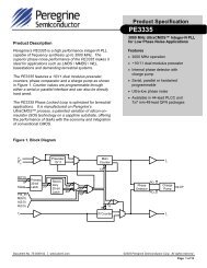
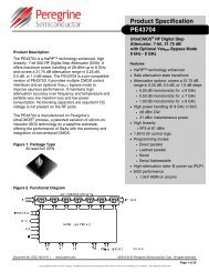
Product Specification<br />
<strong>PE42421</strong><br />
SPDT UltraCMOS ®<br />
10 MHz – 3.0 GHz RF Switch<br />
Product Description<br />
The <strong>PE42421</strong> UltraCMOS ® RF switch is designed to<br />
cover a broad range of applications from 10 MHz<br />
through 3000 MHz. This reflective switch integrates<br />
on-board CMOS control logic with a low voltage<br />
CMOS-compatible control interface, and can be<br />
controlled using either single-pin or complementary<br />
control inputs. Using a nominal +3-volt power supply<br />
voltage, a typical input 1 dB compression point of<br />
+33.5 dBm can be achieved.<br />
The <strong>PE42421</strong> SPDT RF switch is manufactured on<br />
<strong>Peregrine</strong>’s UltraCMOS ® process, a patented<br />
variation of silicon-on-insulator (SOI) technology on<br />
a sapphire substrate, offering the performance of<br />
GaAs with the economy and integration of<br />
conventional CMOS.<br />
Features<br />
Single-pin or complementary CMOS<br />
logic control inputs<br />
Low insertion loss: 0.35 dB at<br />
1000 MHz, 0.5 dB at 2000 MHz<br />
Isolation of 30 dB at 1000 MHz, 20 dB<br />
at 2000 MHz<br />
Typical input 1 dB compression point<br />
of +33.5 dBm<br />
1.8V minimum power supply voltage<br />
SC-70 package<br />
Figure 1. Functional Diagram<br />
RFC<br />
Figure 2. Package<br />
6-lead SC-70<br />
ESD<br />
RF1<br />
ESD<br />
ESD<br />
RF2<br />
CMOS<br />
Control<br />
Driver<br />
CTRL CTRL or V DD<br />
71-0015-01<br />
Document No. 70-0396-03 │ www.psemi.com<br />
©2010-2013 <strong>Peregrine</strong> <strong>Semiconductor</strong> Corp. All rights reserved.<br />
Page 1 of 9<br />
Logo updated under non-rev change. <strong>Peregrine</strong> products are protected under one or more of the following U.S. Patents: http://patents.psemi.com
<strong>PE42421</strong><br />
Product Specification<br />
Table 1. Electrical Specifications @ +25°C, V DD = 3V (Z S = Z L = 50Ω )<br />
Parameter Condition Minimum Typical Maximum Unit<br />
Operation Frequency 1 10 MHz 3000 MHz<br />
Insertion Loss 3<br />
Isolation<br />
Return Loss 3<br />
1000 MHz<br />
2000 MHz<br />
1000 MHz<br />
2000 MHz<br />
1000 MHz<br />
2000 MHz<br />
‘ON’ Switching Time 50% CTRL to 0.1 dB of final value, 1 GHz 1.50 us<br />
‘OFF’ Switching Time 50% CTRL to 25 dB isolation, 1 GHz 1.50 us<br />
Video Feedthrough 2 15 mV pp<br />
Input 1 dB Compression<br />
1000 MHz @ 2.3 - 3.3V<br />
1000 MHz @ 1.8 - 2.3V<br />
2500 MHz @ 2.3 - 3.3V<br />
2500 MHz @ 1.8 - 2.3V<br />
Input IP3 1000 MHz, 20dBm input power 55 dBm<br />
Notes: 1. Device linearity will begin to degrade below 10 MHz<br />
2. The DC transient at the output of any port of the switch when the control voltage is switched from Low to High or High to Low in a 50Ω test set-up, measured with<br />
1ns risetime pulses and 500 MHz bandwidth<br />
3. A tuning capacitor must be added to the application board to optimize the insertion loss and return loss performance. See Figure 6 for details<br />
29<br />
19<br />
21<br />
24<br />
31.5<br />
29.5<br />
28.5<br />
28<br />
0.35<br />
0.50<br />
30<br />
20<br />
22<br />
27<br />
33.5<br />
30.5<br />
30.5<br />
29<br />
0.45<br />
0.60<br />
dB<br />
dB<br />
dB<br />
dB<br />
dB<br />
dB<br />
dBm<br />
©2010-2013 <strong>Peregrine</strong> <strong>Semiconductor</strong> Corp. All rights reserved. Document No. 70-0396-03 │ UltraCMOS ® RFIC Solutions<br />
Page 2 of 9<br />
Logo updated under non-rev change. <strong>Peregrine</strong> products are protected under one or more of the following U.S. Patents: http://patents.psemi.com
<strong>PE42421</strong><br />
Product Specification<br />
Figure 3. Pin Configuration (Top View)<br />
Table 4. Absolute Maximum Ratings<br />
Symbol Parameter/Condition Min Max Unit<br />
V DD Power supply voltage -0.3 4.0 V<br />
Table 2. Pin Descriptions<br />
Pin No. Pin Name Description<br />
1 RF1 4 RF Port1<br />
2 GND<br />
3 RF2 4 RF Port2<br />
Ground connection. Traces should be<br />
physically short and connected to ground<br />
plane for best performance.<br />
4 CTRL Switch control input, CMOS logic level.<br />
5 RFC 4 RF Common<br />
6 CTRL or V DD<br />
This pin supports two interface options:<br />
Single-pin control mode. A nominal 3-volt<br />
supply connection is required.<br />
Complementary-pin control mode. A complementary<br />
CMOS control signal to CTRL<br />
is supplied to this pin. Bypassing on this<br />
pin is not required in this mode.<br />
V I Voltage on any DC input -0.3<br />
V DD +<br />
0.3<br />
T ST Storage temperature range -65 150 °C<br />
T OP<br />
Operating temperature<br />
range<br />
Notes: 5. To maintain optimum device performance, do not exceed Max P IN at<br />
desired operating frequency (see Figure 4)<br />
V<br />
-40 85 °C<br />
P IN Input power (50 Ω) +34 5 dBm<br />
V ESD<br />
ESD Voltage (HBM,<br />
ML_STD 883 Method<br />
3015.7)<br />
ESD Voltage (MM, JEDEC,<br />
JESD22-A114-B)<br />
2000 V<br />
100 V<br />
Exceeding absolute maximum ratings may cause<br />
permanent damage. Operation should be restricted to<br />
the limits in the Operating Ranges table. Operation<br />
between operating range maximum and absolute<br />
maximum for extended periods may reduce reliability.<br />
Figure 4. Maximum Input Power<br />
Note: 4. All RF pins must be DC blocked with an external series capacitor or<br />
held at 0 V DC<br />
Table 3. Operating Ranges<br />
Parameter Min Typ Max Unit<br />
V DD Power Supply Voltage 1.8 3.0 3.3 V<br />
I DD Power Supply Current<br />
(V DD = 3V, V CNTL = 3V)<br />
9 20 µA<br />
Control Voltage High 0.7x V DD V<br />
Control Voltage Low 0.3x V DD V<br />
Moisture Sensitivity Level<br />
The Moisture Sensitivity Level rating for the <strong>PE42421</strong> in<br />
the SC70 package is MSL1.<br />
Switching Frequency<br />
The <strong>PE42421</strong> has a maximum 25 kHz switching rate.<br />
Latch-Up Avoidance<br />
Unlike conventional CMOS devices, UltraCMOS ®<br />
devices are immune to latch-up.<br />
Electrostatic Discharge (ESD) Precautions<br />
When handling this UltraCMOS ® device, observe the<br />
same precautions that you would use with other ESDsensitive<br />
devices. Although this device contains<br />
circuitry to protect it from damage due to ESD,<br />
precautions should be taken to avoid exceeding the<br />
specified rating.<br />
Document No. 70-0396-03 │ www.psemi.com<br />
©2010-2013 <strong>Peregrine</strong> <strong>Semiconductor</strong> Corp. All rights reserved.<br />
Page 3 of 9<br />
Logo updated under non-rev change. <strong>Peregrine</strong> products are protected under one or more of the following U.S. Patents: http://patents.psemi.com
<strong>PE42421</strong><br />
Product Specification<br />
Table 5. Single-pin Control Logic Truth Table<br />
Control Voltages<br />
Pin 6 (V DD ) = V DD<br />
Pin 4 (CTRL) = High<br />
Pin 6 (V DD ) = V DD<br />
Pin 4 (CTRL) = Low<br />
Signal Path<br />
RFC to RF2<br />
RFC to RF1<br />
Table 6. Complementary-pin Control Logic<br />
Truth Table<br />
Control Voltages<br />
Pin 6 (CTRL or V DD ) = Low<br />
Pin 4 (CTRL) = High<br />
Pin 6 (CTRL or V DD ) = High<br />
Pin 4 (CTRL) = Low<br />
Signal Path<br />
RFC to RF2<br />
RFC to RF1<br />
Control Logic Input<br />
The <strong>PE42421</strong> is a versatile RF CMOS switch that<br />
supports two operating control modes; single-pin<br />
control mode and complementary-pin control<br />
mode.<br />
Single-pin control mode enables the switch to<br />
operate with a single control pin (pin 4) supporting<br />
a +3-volt CMOS logic input, and requires a<br />
dedicated +3-volt power supply connection on pin<br />
6 (V DD ). This mode of operation reduces the<br />
number of control lines required and simplifies the<br />
switch control interface typically derived from a<br />
CMOS Processor I/O port.<br />
Complementary-pin control mode allows the<br />
switch to operate using complementary control<br />
pins CTRL and CTRL (pins 4 & 6), that can be<br />
directly driven by +3-volt CMOS logic or a suitable<br />
Processor I/O port. This enables the <strong>PE42421</strong> to<br />
be used as a potential alternate source for SPDT<br />
RF switch products used in positive control<br />
voltage mode and operating within the <strong>PE42421</strong><br />
operating limits.<br />
©2010-2013 <strong>Peregrine</strong> <strong>Semiconductor</strong> Corp. All rights reserved. Document No. 70-0396-03 │ UltraCMOS ® RFIC Solutions<br />
Page 4 of 9<br />
Logo updated under non-rev change. <strong>Peregrine</strong> products are protected under one or more of the following U.S. Patents: http://patents.psemi.com
<strong>PE42421</strong><br />
Product Specification<br />
Evaluation Kit<br />
The SPDT switch EK Board was designed to ease<br />
customer evaluation of <strong>Peregrine</strong>’s <strong>PE42421</strong>. The<br />
RF common port is connected through a 50Ω<br />
transmission line via the top SMA connector, J1.<br />
RF1 and RF2 are connected through 50Ω<br />
transmission lines via SMA connectors J2 and J3,<br />
respectively. A through 50Ω transmission is<br />
available via SMA connectors J4 and J5. This<br />
transmission line can be used to estimate the loss<br />
of the PCB over the environmental conditions<br />
being evaluated.<br />
Figure 5. Evaluation Board Layouts<br />
<strong>Peregrine</strong> Specification 101-0162-02<br />
The board is constructed of a two metal layer FR4<br />
material with a total thickness of 0.031”. The<br />
bottom layer provides ground for the RF<br />
transmission lines. The transmission lines were<br />
designed using a coplanar waveguide with ground<br />
plane model using a trace width of 0.0476”, trace<br />
gaps of 0.030”, dielectric thickness of 0.028”,<br />
metal thickness of 0.0021” and ε r of 4.4.<br />
J6 and J7 provide a means for controlling DC and<br />
digital inputs to the device. J6-1 is connected to<br />
the device V DD or CTRL input. J7-1 is connected<br />
to the device CTRL input.<br />
Figure 6. Evaluation Board Schematic<br />
<strong>Peregrine</strong> Specification 102-0756-01<br />
J4<br />
N/A<br />
1<br />
1<br />
J5<br />
N/A<br />
T-line Description<br />
--<br />
Model = CPWG<br />
H=28mils<br />
T=2.1mils<br />
W=47mils<br />
G=30mils<br />
Er = 4.4<br />
J7<br />
CNTL<br />
1<br />
2<br />
R2<br />
1KOhm<br />
General Comments<br />
Transmission lines connected to J1, J2, and J3 should have exactly the<br />
same electrical length<br />
The path from J2 to J3 including the distance through the part should<br />
have the same length as J4 and J5 and be in parallel to J4 to J5<br />
J1<br />
RFC<br />
C1<br />
0.5pF<br />
SEEASSYNOTE 2<br />
C2<br />
0.5pF<br />
SEEASSYNOTE 2<br />
Document No. 70-0396-03 │ www.psemi.com<br />
1<br />
1<br />
2<br />
1<br />
2<br />
J6<br />
R1<br />
1KOhm<br />
CNTLX/VDD<br />
1<br />
2<br />
U1<br />
<strong>PE42421</strong>/SC70-6<br />
4 CTRL RF_2 3<br />
5 RFC GND 2<br />
6 VDD RF_1 1<br />
©2010-2013 <strong>Peregrine</strong> <strong>Semiconductor</strong> Corp. All rights reserved.<br />
1<br />
1<br />
J3<br />
RF2<br />
J2<br />
RF1<br />
Notes: Add two 0.5 pF caps in series to be shunted on the J1 SMA input<br />
Solder C1 side 1 to the RF trace close to the J1 pin<br />
Solder C1 side 2 to C2 side 1<br />
Solder C2 side 2 to ground<br />
Logo updated under non-rev change. <strong>Peregrine</strong> products are protected under one or more of the following U.S. Patents: http://patents.psemi.com<br />
Page 5 of 9
<strong>PE42421</strong><br />
Product Specification<br />
Typical Performance Data @ -40°C to 85°C (Unless Otherwise Noted)<br />
Figure 7. Insertion Loss<br />
Figure 8. Isolation – Input to Output<br />
Figure 9. Isolation – Output to Output<br />
Figure 10. Return Loss (Input)<br />
©2010-2013 <strong>Peregrine</strong> <strong>Semiconductor</strong> Corp. All rights reserved. Document No. 70-0396-03 │ UltraCMOS ® RFIC Solutions<br />
Page 6 of 9<br />
Logo updated under non-rev change. <strong>Peregrine</strong> products are protected under one or more of the following U.S. Patents: http://patents.psemi.com
<strong>PE42421</strong><br />
Product Specification<br />
Typical Performance Data @ V DD = 2.3V, T = 25°C<br />
Figure 11. Insertion Loss<br />
Figure 12. Isolation – Input to Output<br />
Figure 13. Isolation – Output to Output<br />
Figure 14. Return Loss (Input & Output)<br />
Document No. 70-0396-03 │ www.psemi.com<br />
©2010-2013 <strong>Peregrine</strong> <strong>Semiconductor</strong> Corp. All rights reserved.<br />
Page 7 of 9<br />
Logo updated under non-rev change. <strong>Peregrine</strong> products are protected under one or more of the following U.S. Patents: http://patents.psemi.com
<strong>PE42421</strong><br />
Product Specification<br />
Figure 15. Package Drawing<br />
6-lead SC-70<br />
A<br />
2.10±0.05<br />
1.30<br />
0.10 C<br />
(2X)<br />
0.65<br />
B<br />
6 4<br />
0.50 MIN<br />
0.10 C<br />
1.25±0.10<br />
2.10±0.10<br />
0.90±0.10<br />
1.90<br />
0.10 C<br />
(2X)<br />
1 3<br />
0.05 C<br />
SEATING PLANE<br />
0.05±0.05<br />
C<br />
Pin #1 Corner<br />
0.65<br />
Top View<br />
0.225±0.075<br />
Side View<br />
0.40 MIN<br />
1.30<br />
Recommended Land Pattern<br />
0.10 A B<br />
181-0013<br />
0.165±0.085<br />
ALL FEATURES<br />
0.36±0.10<br />
End View<br />
Figure 16. Top Marking Specification<br />
PPP<br />
YWW<br />
= Pin 1 Indicator<br />
PPP = Part Number<br />
YWW = Date Code<br />
17-0021<br />
©2010-2013 <strong>Peregrine</strong> <strong>Semiconductor</strong> Corp. All rights reserved. Document No. 70-0396-03 │ UltraCMOS ® RFIC Solutions<br />
Page 8 of 9<br />
Logo updated under non-rev change. <strong>Peregrine</strong> products are protected under one or more of the following U.S. Patents: http://patents.psemi.com
6<br />
1<br />
5<br />
2<br />
6<br />
1<br />
5<br />
2<br />
<strong>PE42421</strong><br />
Product Specification<br />
Figure 17. Tape and Reel Specifications<br />
Pin 1<br />
Tape Feed Direction<br />
3 4<br />
Top of<br />
Device<br />
3 4<br />
Pin 1<br />
Device Orientation in Tape<br />
Table 7. Ordering Information<br />
Order Code Part Marking Description Package Shipping Method<br />
EK42421-01 <strong>PE42421</strong>-EK <strong>PE42421</strong> Evaluation Kit Evaluation Kit 1 / Box<br />
<strong>PE42421</strong>SCAA-Z 421 <strong>PE42421</strong> SPDT RF Switch Green 6-lead SC-70 3000 units / T&R<br />
Sales Contact and Information<br />
For sales and contact information please visit www.psemi.com.<br />
Advance Information: The product is in a formative or design stage. The datasheet contains design target<br />
specifications for product development. Specifications and features may change in any manner without notice.<br />
Preliminary Specification: The datasheet contains preliminary data. Additional data may be added at a later<br />
date. <strong>Peregrine</strong> reserves the right to change specifications at any time without notice in order to supply the best<br />
possible product. Product Specification: The datasheet contains final data. In the event <strong>Peregrine</strong> decides to<br />
change the specifications, <strong>Peregrine</strong> will notify customers of the intended changes by issuing a CNF (Customer<br />
Notification Form).<br />
The information in this datasheet is believed to be reliable. However, <strong>Peregrine</strong> assumes no liability for the use<br />
of this information. Use shall be entirely at the user’s own risk.<br />
No patent rights or licenses to any circuits described in this datasheet are implied or granted to any third party.<br />
<strong>Peregrine</strong>’s products are not designed or intended for use in devices or systems intended for surgical implant,<br />
or in other applications intended to support or sustain life, or in any application in which the failure of the<br />
<strong>Peregrine</strong> product could create a situation in which personal injury or death might occur. <strong>Peregrine</strong> assumes no<br />
liability for damages, including consequential or incidental damages, arising out of the use of its products in<br />
such applications.<br />
The <strong>Peregrine</strong> name, logo, UltraCMOS and UTSi are registered trademarks and HaRP, MultiSwitch and DuNE<br />
are trademarks of <strong>Peregrine</strong> <strong>Semiconductor</strong> Corp.<br />
Document No. 70-0396-03 │ www.psemi.com<br />
©2010-2013 <strong>Peregrine</strong> <strong>Semiconductor</strong> Corp. All rights reserved.<br />
Page 9 of 9<br />
Logo updated under non-rev change. <strong>Peregrine</strong> products are protected under one or more of the following U.S. Patents: http://patents.psemi.com