SILICON NPN POWER DARLINGTON TRANSISTOR
SILICON NPN POWER DARLINGTON TRANSISTOR
SILICON NPN POWER DARLINGTON TRANSISTOR

Create successful ePaper yourself
Turn your PDF publications into a flip-book with our unique Google optimized e-Paper software.
®<br />
2N6388<br />
<strong>SILICON</strong> <strong>NPN</strong> <strong>POWER</strong> <strong>DARLINGTON</strong> <strong>TRANSISTOR</strong><br />
■<br />
■<br />
■<br />
■<br />
STMicroelectronics PREFERRED<br />
SALESTYPE<br />
<strong>NPN</strong> <strong>DARLINGTON</strong><br />
HIGH CURRENT CAPABILITY<br />
INTEGRATED ANTIPARALLEL<br />
COLLECTOR-EMITTER DIODE<br />
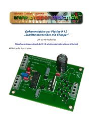
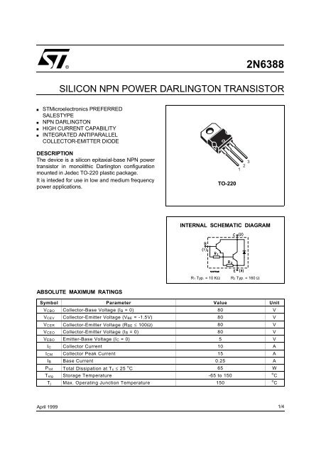
DESCRIPTION<br />
The device is a silicon epitaxial-base <strong>NPN</strong> power<br />
transistor in monolithic Darlington configuration<br />
mounted in Jedec TO-220 plastic package.<br />
It is inteded for use in low and medium frequency<br />
power applications.<br />
TO-220<br />
1 2 3<br />
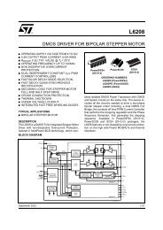
INTERNAL SCHEMATIC DIAGRAM<br />
R1 Typ. = 10 KΩ<br />
R2 Typ. = 160 Ω<br />
ABSOLUTE MAXIMUM RATINGS<br />
Symbol Parameter Value Unit<br />
V CBO Collector-Base Voltage (I B = 0) 80 V<br />
V CEV Collector-Emitter Voltage (V BE = -1.5V) 80 V<br />
VCER Collector-Emitter Voltage (RBE ≤ 100Ω) 80 V<br />
VCEO Collector-Emitter Voltage (IB = 0) 80 V<br />
VEBO Emitter-Base Voltage (IC = 0) 5 V<br />
I C Collector Current 10 A<br />
I CM Collector Peak Current 15 A<br />
I B Base Current 0.25 A<br />
P tot Total Dissipation at Tc ≤ 25 o C 65 W<br />
Tstg Storage Temperature -65 to 150<br />
T j Max. Operating Junction Temperature 150<br />
o C<br />
o C<br />
April 1999<br />
1/4
2N6388<br />
THERMAL DATA<br />
R thj-case Thermal Resistance Junction-case Max 1.92<br />
o C/W<br />
ELECTRICAL CHARACTERISTICS (Tcase = 25 o C unless otherwise specified)<br />
Symbol Parameter Test Conditions Min. Typ. Max. Unit<br />
I CEV<br />
I CEO<br />
I EBO<br />
V CEO(sus)∗<br />
V CER(sus)∗<br />
V CEV(sus)∗<br />
V CE(sat)∗<br />
Collector Cut-off<br />
Current (VBE = -1.5V)<br />
Collector Cut-off<br />
Current (IB = 0)<br />
Emitter Cut-off Current<br />
(IC = 0)<br />
Collector-Emitter<br />
Sustaining Voltage<br />
Collector-Emitter<br />
Sustaining Voltage<br />
Collector-Emitter<br />
Sustaining Voltage<br />
V CE = rated V CEO<br />
VCE = rated VCEO Tc = 125 o C<br />
Collector-Emitter I C = 5 A I B = 10 mA<br />
Saturation Voltage IC = 10 A IB = 100 mA<br />
V BE∗ Base-Emitter Voltage I C = 5 A V CE = 3 V<br />
IC = 10 A VCE = 3 V<br />
h FE∗ DC Current Gain I C = 5 A V CE = 3 V<br />
IC = 10 A VCE = 3 V<br />
h fe<br />
VF∗<br />
C CBO<br />
I s/b∗∗<br />
Es/b<br />
Small Signal Current<br />
Gain<br />
Parallel-diode Forward<br />
Voltage<br />
Collector Base<br />
Capacitance<br />
Second Breakdown<br />
Collector Current<br />
Second Breakdown<br />
Energy<br />
0.3<br />
3<br />
mA<br />
mA<br />
V CE = 80 V 1 mA<br />
V EB = 5 V 5 mA<br />
I C = 200 mA 80 V<br />
I C = 200 mA R BE = 100 Ω 80 V<br />
I C = 200 mA V BE = -1.5V 80 V<br />
I C = 1 A V CE = 10 V f = 1MHz<br />
I C = 1 A V CE = 10 V f = 1KHz<br />
1000<br />
100<br />
20<br />
1000<br />
2<br />
3<br />
2.8<br />
4.5<br />
20000<br />
IF = 10 A 4 V<br />
I E = 0 V CB = 10 V f = 1MHz 200 pF<br />
V CE = 25 V 2.6 A<br />
L = 12 mH<br />
V BE = -1.5 V<br />
∗ Pulsed: Pulse duration = 300 µs, duty cycle 1.5 %<br />
∗∗ Pulsed: Pulse duration = 100ms non repetitive pulse.<br />
R BE = 100 Ω<br />
I C = 4.5 A<br />
V<br />
V<br />
V<br />
V<br />
120 mJ<br />
2/4
2N6388<br />
TO-220 MECHANICAL DATA<br />
DIM.<br />
mm<br />
inch<br />
MIN. TYP. MAX. MIN. TYP. MAX.<br />
A 4.40 4.60 0.173 0.181<br />
C 1.23 1.32 0.048 0.051<br />
D 2.40 2.72 0.094 0.107<br />
D1 1.27 0.050<br />
E 0.49 0.70 0.019 0.027<br />
F 0.61 0.88 0.024 0.034<br />
F1 1.14 1.70 0.044 0.067<br />
F2 1.14 1.70 0.044 0.067<br />
G 4.95 5.15 0.194 0.203<br />
G1 2.4 2.7 0.094 0.106<br />
H2 10.0 10.40 0.393 0.409<br />
L2 16.4 0.645<br />
L4 13.0 14.0 0.511 0.551<br />
L5 2.65 2.95 0.104 0.116<br />
L6 15.25 15.75 0.600 0.620<br />
L7 6.2 6.6 0.244 0.260<br />
L9 3.5 3.93 0.137 0.154<br />
DIA. 3.75 3.85 0.147 0.151<br />
P011C<br />
3/4
2N6388<br />
Information furnished is believed to be accurate and reliable. However, STMicroelectronics assumes no responsibility for the consequences<br />
of use of such information nor for any infringement of patents or other rights of third parties which may result from its use. No license is<br />
granted by implication or otherwise under any patent or patent rights of STMicroelectronics. Specification mentioned in this publication are<br />
subject to change without notice. This publication supersedes and replaces all information previously supplied. STMicroelectronics products<br />
are not authorized for use as critical components in life support devices or systems without express written approval of STMicroelectronics.<br />
The ST logo is a trademark of STMicroelectronics<br />
© 1999 STMicroelectronics – Printed in Italy – All Rights Reserved<br />
STMicroelectronics GROUP OF COMPANIES<br />
Australia - Brazil - Canada - China - France - Germany - Italy - Japan - Korea - Malaysia - Malta - Mexico - Morocco - The Netherlands -<br />
Singapore - Spain - Sweden - Switzerland - Taiwan - Thailand - United Kingdom - U.S.A.<br />
4/4<br />
http://www.st.com<br />
.