Chapter 1 : Introduction to the HC12 Microcontroller - EngSoc
Chapter 1 : Introduction to the HC12 Microcontroller - EngSoc
Chapter 1 : Introduction to the HC12 Microcontroller - EngSoc

You also want an ePaper? Increase the reach of your titles
YUMPU automatically turns print PDFs into web optimized ePapers that Google loves.
The 68<strong>HC12</strong> <strong>Microcontroller</strong><br />
<strong>Chapter</strong> 1<br />
<strong>Introduction</strong> <strong>to</strong> 68<strong>HC12</strong><br />
Assembly Notation :<br />
Intel<br />
Mo<strong>to</strong>rola<br />
binary 10010011b %10010011<br />
decimal 1478 1478<br />
hexadecimal 5678h $5678<br />
H. Huang Transparency No.1-1<br />
The 68<strong>HC12</strong> <strong>Microcontroller</strong><br />
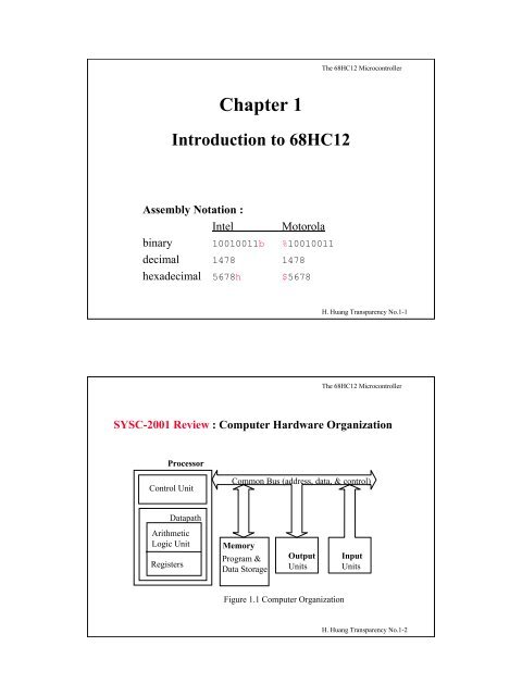
SYSC-2001 Review : Computer Hardware Organization<br />
Processor<br />
Control Unit<br />
Common Bus (address, data, & control)<br />
Datapath<br />
Arithmetic<br />
Logic Unit<br />
Registers<br />
Memory<br />
Program &<br />
Data S<strong>to</strong>rage<br />
Output<br />
Units<br />
Input<br />
Units<br />
Figure 1.1 Computer Organization<br />
H. Huang Transparency No.1-2
The 68<strong>HC12</strong> <strong>Microcontroller</strong><br />
CPU: Microprocessor versus <strong>Microcontroller</strong><br />
• Microprocessor: processor on a single integrated chip<br />
– Intel 80x86, Mo<strong>to</strong>rola 680x0 families...<br />
• Microprocessors evolved in two general directions:<br />
– Performance: processing power, data s<strong>to</strong>rage<br />
– Integration: amount of circuits on one chip<br />
• Microcomputer: computer using microprocessor as CPU<br />
– Combines microprocessor/peripheral chips -> computer system<br />
– i.e.: PC => Intel 80x86 + memory + timer + keyboard +<br />
modem (etc.) chips<br />
• <strong>Microcontroller</strong>: computer system on a chip<br />
– Microprocessor AND peripheral functions implemented on one chip<br />
– Built-in memory and interface circuits (I/O units)<br />
H. Huang Transparency No.1-3<br />
The 68<strong>HC12</strong> <strong>Microcontroller</strong><br />
MicroComputer versus MicroController System<br />
Micro<br />
Processor<br />
CPU<br />
Memory<br />
I/O Components<br />
Power<br />
Clock<br />
Micro<br />
Processor<br />
CPU<br />
Memory<br />
I/O Components<br />
Power<br />
Clock<br />
Extended<br />
Memory<br />
O<strong>the</strong>r I/O<br />
Peripheral<br />
H. Huang Transparency No.1-4
The 68<strong>HC12</strong> <strong>Microcontroller</strong><br />
Features of <strong>the</strong> 68<strong>HC12</strong> <strong>Microcontroller</strong><br />
- 16-bit CPU<br />
- 64 Kb memory space<br />
- 768 bytes <strong>to</strong> 4 Kb of EEPROM<br />
- 1 Kb <strong>to</strong> 12 Kb of on-chip SRAM<br />
- 32 Kb <strong>to</strong> 128 Kb flash memory<br />
- Sophisticated timer functions including: input capture, output<br />
compare, pulse accumula<strong>to</strong>rs, real-time interrupt, COP timer<br />
- Serial communication interfaces: SCI, SPI, CAN, BDLC<br />
- Background debug mode (BDM)<br />
- 8-bit or 10-bit A/D converter<br />
- Instructions for supporting fuzzy logic function<br />
H. Huang Transparency No.1-5<br />
Block Diagram of MC68<strong>HC12</strong><br />
The 68<strong>HC12</strong> <strong>Microcontroller</strong><br />
PAD0<br />
EEPROM<br />
A/D Converter<br />
Port AD<br />
RAM<br />
FLASH<br />
CPU12<br />
Timer &<br />
Pulse Accumula<strong>to</strong>r<br />
SCI<br />
I/O<br />
SPI<br />
PWM<br />
I/O<br />
PT0<br />
PS0<br />
PP0<br />
Port T<br />
Port S<br />
Port P<br />
Port A* Port B* * Multiplex : Simple I/O or Extended Address/Data<br />
H. Huang Transparency No.1-6
The 68<strong>HC12</strong> Family<br />
The 68<strong>HC12</strong> <strong>Microcontroller</strong><br />
• 68<strong>HC12</strong> Family Members<br />
– Different memory and number/type of on-chip peripheral<br />
functions<br />
– Vary in fabrication methods (different power requirements,<br />
environmental <strong>to</strong>lerances, cost)<br />
Huang Text : CME-12BC32<br />
• Made from socket parts<br />
• One SCI channel<br />
• 1 A/D Converter<br />
Our lab : CML-9S12DP256<br />
• Made from surface-mount parts<br />
• Two SCI Channels<br />
• 2 A/D Converters<br />
Concepts : Use Text<br />
Specifics : Use Hardware Reference Manuals (posted on website)<br />
H. Huang Transparency No.1-7<br />
<strong>HC12</strong> Programmer’s Model<br />
The 68<strong>HC12</strong> <strong>Microcontroller</strong><br />
7 A 07 B 0 8-bit accumula<strong>to</strong>r A and B<br />
15 D 0<br />
or<br />
16-bit double accumula<strong>to</strong>r D<br />
15 X 0<br />
15 Y 0<br />
15 SP 0<br />
Index register X<br />
Index register Y<br />
Stack pointer<br />
15 PC 0<br />
Program counter<br />
Figure 1.3 MC68<strong>HC12</strong> CPU registers.<br />
H. Huang Transparency No.1-8
Condition Code Register<br />
The 68<strong>HC12</strong> <strong>Microcontroller</strong><br />
7 6 5 4 3 2 1 0<br />
S X H I N Z V C<br />
Figure 2.8 Condition code register<br />
C : Carry Flag<br />
Set if carry generated as a result of an operation<br />
V : Overflow Flag<br />
Sets if result of 2’s complement arithmetic operation is out of range<br />
Z : Zero Flag<br />
Set if result of an operation is zero<br />
N : Negative Flag<br />
Set if MSB of <strong>the</strong> result of an operation = 1<br />
H : Half-carry Flag<br />
Set if carry from lower four bits <strong>to</strong> upper four bits as a result<br />
of an operation<br />
H. Huang Transparency No.1-9<br />
Instruction Set<br />
- 68<strong>HC12</strong> instructions: one/two bytes -> opcode; zero-five bytes<br />
-> operand (addressing information).<br />
The 68<strong>HC12</strong> <strong>Microcontroller</strong><br />
Opcode<br />
$18 Opcode<br />
Operands<br />
- Opcode: operation <strong>to</strong> be performed. First byte of two-byte opcode always $18.<br />
- Instruction (opcodes) classified in<strong>to</strong> three groups<br />
1. Data Transfer<br />
2. Data Manipulation (Arithmetic and Logic)<br />
3. Control Flow<br />
H. Huang Transparency No.1-10
The 68<strong>HC12</strong> <strong>Microcontroller</strong><br />
Source Code<br />
- Program written in assembly or high-level language<br />
Object Code<br />
Output of an assembler or compiler<br />
- Executable program in binary format (machine instructions)<br />
line<br />
addr.<br />
machine code<br />
(Assembly)source code<br />
1:<br />
1000<br />
= 00001000<br />
org $1000<br />
2:<br />
1003<br />
B6 0800<br />
ldaa $800<br />
3:<br />
1006<br />
BB 0801<br />
adda $801<br />
4:<br />
1009<br />
BB 0802<br />
adda $802<br />
6:<br />
7A 0900<br />
staa $900<br />
end<br />
H. Huang Transparency No.1-11<br />
The 68<strong>HC12</strong> <strong>Microcontroller</strong><br />
Memory Format of <strong>the</strong> 68<strong>HC12</strong> family<br />
• <strong>HC12</strong>: 16-bit processor. It can read 16-bit words<br />
organized as 8-bit bytes.<br />
– On Mo<strong>to</strong>rola’s, words accessed with Big Endian format<br />
Memory<br />
Address<br />
1202<br />
Address<br />
$1200<br />
$1201<br />
$1202<br />
$1203<br />
$1204<br />
Data<br />
5E<br />
73<br />
A2<br />
95<br />
0A<br />
Byte at Address 1202 = $A2<br />
Word at Address 1202 = $A295<br />
%1010 0010<br />
Big Endian<br />
Data is 8 bits<br />
H. Huang Transparency No.1-12
MC68<strong>HC12</strong> Memory Map<br />
The 68<strong>HC12</strong> <strong>Microcontroller</strong><br />
• Different members of <strong>the</strong> <strong>HC12</strong> family: different amounts of on-chip<br />
SRAM, EEPROM and flash memory<br />
• Education boards: external SRAM and EEPROM <strong>to</strong> facilitate<br />
program downloading/debugging<br />
• <strong>HC12</strong> can only access 64Kbytes of memory (16-bit processor).<br />
Larger memory spaces: special “bank-switching” techniques<br />
• Memory mapped <strong>to</strong> allocate different kinds of data and instructions<br />
(single-chip; expanded mode)<br />
• More information about memory mapping: board’s user manual.<br />
H. Huang Transparency No.1-13<br />
The 68<strong>HC12</strong> <strong>Microcontroller</strong><br />
MC68<strong>HC12</strong> Memory Map (Huang p.105)<br />
FFFF<br />
FFFE<br />
Reset Vec<strong>to</strong>r Address<br />
External EPROM OR<br />
External SRAM OR<br />
Internal Flash EEPROM<br />
8000<br />
7FFF External RAM (if configured)<br />
1000<br />
0FFF <strong>HC12</strong> Internal EEPROM<br />
D00<br />
CFF<br />
C00<br />
External RAM (if configured)<br />
BFF<br />
Internal SRAM<br />
800<br />
7FF<br />
400 External SRAM (if configured)<br />
3FF<br />
200 Peripheral Area<br />
1FF<br />
0000 <strong>HC12</strong> Internal Registers<br />
H. Huang Transparency No.1-14
MC68<strong>HC12</strong> Memory Map for DP256 (In <strong>the</strong> lab)<br />
FFFF<br />
FF00<br />
8000<br />
7FFF<br />
4000<br />
3FFF<br />
1000<br />
0FFF<br />
Vec<strong>to</strong>r Address<br />
EEPROM and Flash<br />
16kbytes External RAM<br />
12Kbytes Internal RAM<br />
4kbytes Internal EEPROM<br />
The 68<strong>HC12</strong> <strong>Microcontroller</strong><br />
400<br />
3FF<br />
200<br />
1FF<br />
0000<br />
Peripheral Area<br />
<strong>HC12</strong> Internal Registers<br />
H. Huang Transparency No.1-15<br />
<strong>HC12</strong> Simula<strong>to</strong>r<br />
The 68<strong>HC12</strong> <strong>Microcontroller</strong><br />
• <strong>Microcontroller</strong> simula<strong>to</strong>r: <strong>to</strong>ol (program) that replicates<br />
<strong>the</strong> operation of a microcontroller<br />
– Learn about/ develop code without having <strong>the</strong> hardware<br />
• <strong>HC12</strong> simula<strong>to</strong>r mimics operation of <strong>HC12</strong> microcontroller<br />
– Displays and changes “registers”<br />
– Displays and changes “memory”<br />
– “Executes” code, changing contents of simulated memory/ registers<br />
according <strong>to</strong> <strong>the</strong> semantics of instructions executed<br />
H. Huang Transparency No.1-16
The 68<strong>HC12</strong> <strong>Microcontroller</strong><br />
<strong>HC12</strong> Simula<strong>to</strong>r<br />
We will use a freeware simula<strong>to</strong>r available at<br />
http://www.electronikladen.de/hc12<br />
This simula<strong>to</strong>r is a Java program, so you will need <strong>to</strong> have a JDK on your<br />
machine<br />
www.sun.org<br />
Instructions for running <strong>the</strong> simula<strong>to</strong>r are provided in a note on <strong>the</strong> course<br />
webpage.<br />
H. Huang Transparency No.1-17<br />
The 68<strong>HC12</strong> <strong>Microcontroller</strong><br />
Simula<strong>to</strong>r Demo<br />
H. Huang Transparency No.1-18
I/O Ports and I/O Addresses<br />
The 68<strong>HC12</strong> <strong>Microcontroller</strong><br />
Enable exchange of data between chip and external I/O devices<br />
- A port for a particular device identified by I/O Address<br />
Address<br />
Decoder<br />
Micro<br />
processor<br />
CE<br />
Interface<br />
chip 1<br />
CE<br />
Interface<br />
chip 1<br />
Data Bus<br />
Figure 7.1 Interface chip, I/O devices, and microprocessor<br />
H. Huang Transparency No.1-19<br />
The 68<strong>HC12</strong> <strong>Microcontroller</strong><br />
I/O Addressing Schemes: Isolated I/O<br />
- Based on a separate address space for I/O devices.<br />
- Programming: use dedicated instructions for I/O operations.<br />
Control (RD/WR)<br />
Processor<br />
Data<br />
Address<br />
Memory<br />
Memory Map<br />
FFFF<br />
0xFF<br />
0000<br />
I/O Map<br />
I/O Device<br />
I/O Control (IOR/IOW)<br />
0000<br />
H. Huang Transparency No.1-20
The 68<strong>HC12</strong> <strong>Microcontroller</strong><br />
I/O Addressing Scheme : Memory Mapped I/O<br />
• Both I/O and memory shared same memory space.<br />
• Programmer’s: same instructions for both memory and I/O<br />
Control (RD/WR)<br />
Processor<br />
Data<br />
Address<br />
Memory<br />
FFFF<br />
Memory Map<br />
I/O Map<br />
I/O Device<br />
0000<br />
H. Huang Transparency No.1-21<br />
Using a High-level Language<br />
The 68<strong>HC12</strong> <strong>Microcontroller</strong><br />
Programming MicroControllers<br />
• Syntax: closer <strong>to</strong> human languages<br />
• Transla<strong>to</strong>r (Compiler): convert program in high-level language in<strong>to</strong> machine language<br />
• Allow <strong>the</strong> users <strong>to</strong> work on <strong>the</strong> program logic at higher level.<br />
Machine Language (executable code)<br />
• Sequence of binary digits that can be executed by <strong>the</strong> processor<br />
Assembly Language (mnemonic code)<br />
• Assembly instruction: representation of a machine instruction<br />
(1 assembly instruction = 1 machine instruction)<br />
• Hard <strong>to</strong> understand, program, and debug for humans<br />
Real-Time Embedded Systems programming<br />
• High level languages not adequate: performance issues<br />
• Memory space (Java exe >> C exe >> Assembly exe = machine exe)<br />
H. Huang Transparency No.1-22
The 68<strong>HC12</strong> <strong>Microcontroller</strong><br />
68<strong>HC12</strong> Instruction Examples: Load and S<strong>to</strong>re<br />
- LOAD: copies contents of operand in<strong>to</strong> CPU register.<br />
- STORE: save contents of CPU register in<strong>to</strong> memory location.<br />
- Execution affects certain flags<br />
- N and Z flags of <strong>the</strong> CCR au<strong>to</strong>matically updated; V flag cleared.<br />
Learning <strong>HC12</strong> Instructions : (1) Built-in Operands<br />
Mnemonic Function Operation<br />
STAA<br />
STAB<br />
STD<br />
STS<br />
STX<br />
STY<br />
S<strong>to</strong>re A<br />
S<strong>to</strong>re B<br />
S<strong>to</strong>re D<br />
S<strong>to</strong>re SP<br />
S<strong>to</strong>re X<br />
S<strong>to</strong>re Y<br />
(A) ⇒M<br />
(B) ⇒M<br />
(A) ⇒M, (B) ⇒M+1<br />
(SP) ⇒ M, M+1<br />
(X) ⇒M:M+1<br />
(Y) ⇒M:M+1<br />
H. Huang Transparency No.1-23<br />
The 68<strong>HC12</strong> <strong>Microcontroller</strong><br />
Learning New <strong>HC12</strong> Instructions (1) : Built-in Operands<br />
Mnemonic Function<br />
LDAA Load A<br />
LDAB Load B<br />
LDD Load D<br />
LDS Load SP<br />
LDX Load index register X<br />
LDY Load index register Y<br />
LEAS Load effective address in<strong>to</strong> SP<br />
LEAX Load effective address in<strong>to</strong> X<br />
LEAY Load effective address in<strong>to</strong> Y<br />
Operation<br />
(M) ⇒ A<br />
(M) ⇒B<br />
(M:M+1) ⇒(A:B)<br />
(M:M+1) ⇒SP<br />
(M:M+1) ⇒ X<br />
(M:M+1) ⇒ X<br />
Effective address ⇒SP<br />
Effective address ⇒X<br />
Effective address ⇒Y<br />
H. Huang Transparency No.1-24
The 68<strong>HC12</strong> <strong>Microcontroller</strong><br />
Flags = SXHINZVC<br />
Learning New <strong>HC12</strong> Instructions (2) : Addressing Modes<br />
Source<br />
Operation<br />
Mode<br />
Coding<br />
Flags<br />
LDAA #opr8i<br />
(M)=>A<br />
IMM<br />
86 ii<br />
----xx0-<br />
LDAA opr8a<br />
Load Accumula<strong>to</strong>r A<br />
DIR<br />
96 ii<br />
LDAA opr16a<br />
EXT<br />
B6 hh ll<br />
LDAA oprx0_xysp<br />
IDX<br />
A6 xb<br />
LDAA oprx9, xysp<br />
IDX1<br />
A6 xb ff<br />
LDAA oprx16,xysp<br />
IDX2<br />
A6 xb ee ff<br />
LDAA [D, xysp]<br />
[D,IDX]<br />
A6 xb<br />
LDAA<br />
[oprx16,xysp]<br />
[IDX2]<br />
A6 xb ee ff<br />
H. Huang Transparency No.1-25<br />
The 68<strong>HC12</strong> <strong>Microcontroller</strong><br />
Inherent Addressing Mode<br />
Addressing Modes<br />
- Instructions do not use extra bytes for operands: instructions<br />
ei<strong>the</strong>r do not need operands or all operands are<br />
CPU registers.<br />
- Operands are implied by <strong>the</strong> opcode.<br />
- Examples:<br />
NOP<br />
INX<br />
DECA<br />
H. Huang Transparency No.1-26
The 68<strong>HC12</strong> <strong>Microcontroller</strong><br />
Immediate Addressing Mode<br />
- Operands included in <strong>the</strong> instruction.<br />
- CPU does not access memory for operands.<br />
- Examples:<br />
LDAA #$55<br />
LDX #$800<br />
Operand Compatibility :<br />
- What if we now have LDX #$55 ?<br />
Instruction encoding :<br />
• LDAA #$55 86 55<br />
• LDX #$55 CE 00 55<br />
- What’s wrong with this ? LDAA #$1234<br />
H. Huang Transparency No.1-27<br />
The 68<strong>HC12</strong> <strong>Microcontroller</strong><br />
Direct Addressing Mode<br />
- Can only specify memory locations in <strong>the</strong> range of 0– 255.<br />
- Uses only one byte <strong>to</strong> specify <strong>the</strong> operand address.<br />
- Examples:<br />
LDAA $20<br />
LDAB $40<br />
Extended Addressing Mode<br />
- Full 16-bit address provided in <strong>the</strong> instruction.<br />
- Examples:<br />
LDAA $4000<br />
LDX<br />
$FE60<br />
H. Huang Transparency No.1-28
Indexed Addressing Mode(s)<br />
The 68<strong>HC12</strong> <strong>Microcontroller</strong><br />
• Operand tells how <strong>to</strong> calculate effective address of <strong>the</strong> data<br />
• Many forms calculate address as sum of parts<br />
• Parts = registers and/or constants.<br />
• Effective address = Sum of index register (X, Y, PC, or SP) and<br />
offset <strong>to</strong> specify address of an operand.<br />
• Offset can be 5-bit, 9-bit, and 16-bit signed value or value in<br />
accumula<strong>to</strong>r A, B, or D<br />
Hence, <strong>the</strong> many different forms …<br />
H. Huang Transparency No.1-29<br />
The Various Forms of Indexed Addressing<br />
The 68<strong>HC12</strong> <strong>Microcontroller</strong><br />
1. 5-bit Constant Offset (Indexed Addressing)<br />
Examples : ldaa 0,X<br />
stab -8,X<br />
The range of <strong>the</strong> offset : -16 <strong>to</strong> +15.<br />
2. 9-bit Constant Offset<br />
Examples : ldaa $FF,X<br />
ldab -20,Y<br />
The range of <strong>the</strong> offset : -256 <strong>to</strong> +255<br />
3. 16-bit Constant Offset<br />
Examples: ldaa 2000,X staa 4000,Y<br />
Allows access any location in <strong>the</strong> 64-KB range<br />
4. Accumula<strong>to</strong>r Offset<br />
Examples: ldaa B,X stab B,Y<br />
The offset is contained in ei<strong>the</strong>r A, B or <strong>the</strong> 16-bit accumula<strong>to</strong>r D.<br />
H. Huang Transparency No.1-30
The 68<strong>HC12</strong> <strong>Microcontroller</strong><br />
16-bit Constant Indirect Indexed Addressing Mode<br />
- 16-bit offset added <strong>to</strong> index register <strong>to</strong> form address of memory<br />
location containing a pointer <strong>to</strong> memory location affected by<br />
<strong>the</strong> instruction.<br />
- Square brackets distinguish this addressing mode from 16-bit<br />
constant offset indexing. For example,<br />
LDAA [10,X]<br />
STAA [20,Y]<br />
Compare : LDAA 10, X<br />
LDAA [10,X]<br />
H. Huang Transparency No.1-31<br />
The 68<strong>HC12</strong> <strong>Microcontroller</strong><br />
16-bit Constant Indirect Indexed Addressing (example)<br />
0000<br />
…<br />
0010 10<br />
0011 22<br />
…<br />
0020 2f<br />
0021 10<br />
0022 ff<br />
LDAA 10, X ; Suppose X=0001<br />
; A
Transfer and Exchange Instructions<br />
The 68<strong>HC12</strong> <strong>Microcontroller</strong><br />
- Copy <strong>the</strong> contents of a CPU register or accumula<strong>to</strong>r in<strong>to</strong><br />
ano<strong>the</strong>r CPU register or accumula<strong>to</strong>r.<br />
1. Universal Transfer Instruction: TFR abcdxys, abcdxys<br />
TFR A, B Transfers contents of A <strong>to</strong> B<br />
• TFR does not affect any flags.<br />
2. Specific Transfer Instructions<br />
TAB Transfers contents of A <strong>to</strong> B<br />
TBA Transfer contents of B <strong>to</strong> A<br />
• Both affect <strong>the</strong> N, Z, and V condition code bits.<br />
H. Huang Transparency No.1-33<br />
Transfer and Exchange Instructions<br />
The 68<strong>HC12</strong> <strong>Microcontroller</strong><br />
3. Exchange contents of a pair of registers or accumula<strong>to</strong>rs.<br />
EXG A, B Swap contents of A and B<br />
4. Sign-extend 8-bit two’s complement number in<strong>to</strong> a 16- bit<br />
number<br />
SEX A,X Move contents of A in<strong>to</strong> LSB of X,<br />
and sign extend<br />
• Purpose: To use an 8-bit value in 16-bit signed operations.<br />
H. Huang Transparency No.1-34
The 68<strong>HC12</strong> <strong>Microcontroller</strong><br />
Move Instructions<br />
- Move data bytes or words from a source <strong>to</strong> a destination in memory.<br />
- Six combinations of immediate, extended, and index addressing modes<br />
allowed <strong>to</strong> specify source/destination addresses:<br />
IMM ⇒ EXT, IMM ⇒ IDX, EXT ⇒ EXT,<br />
EXT ⇒ IDX, IDX ⇒ EXT, IDX ⇒ IDX<br />
-Examples:<br />
MOVB $100,$800<br />
MOVW 0,X, 0,Y<br />
H. Huang Transparency No.1-35<br />
The 68<strong>HC12</strong> <strong>Microcontroller</strong><br />
Add and Subtract Instructions<br />
Flags = SXHINZVC<br />
• Destinations of <strong>the</strong>se instructions are always a CPU register or accumula<strong>to</strong>r.<br />
Source<br />
Operation<br />
Mode<br />
Coding<br />
Flags<br />
ADDA #opr8i<br />
(A)+(M)=>A<br />
IMM<br />
8B ii<br />
- - x – x x x x<br />
ADDA opr8a<br />
Add w/o Carry <strong>to</strong> A<br />
DIR<br />
9B ii<br />
ADDA opr16a<br />
EXT<br />
BB hh ll<br />
ADDA oprx0_xysp<br />
IDX<br />
AB xb<br />
ADDA oprx9, xysp<br />
IDX1<br />
AB xb ff<br />
ADDA<br />
oprx16,xysp<br />
ADDA [D, xysp]<br />
IDX2<br />
[D,IDX]<br />
AB xb ee<br />
ff<br />
AB xb<br />
ADDA<br />
[oprx16,xysp]<br />
[IDX2]<br />
AB xb ee<br />
ff<br />
H. Huang Transparency No.1-36
The 68<strong>HC12</strong> <strong>Microcontroller</strong><br />
Variations of <strong>the</strong> Same Theme<br />
Adding TO OTHER registers<br />
adda $800 ; A ⇐ [A] + [$800]<br />
addb $800 ; B ⇐ [B] + [$800]<br />
addd $800 ; D ⇐ [D] + [$800]<br />
Adding TWO registers<br />
WORD!<br />
aba<br />
abx<br />
aby<br />
; A ⇐ [A] + [B]<br />
; X ⇐ [B] + [X]<br />
; Y ⇐ [B] + [Y]<br />
Notice : Order<br />
of operands<br />
H. Huang Transparency No.1-37<br />
The 68<strong>HC12</strong> <strong>Microcontroller</strong><br />
Addition Overflow<br />
Problem: Fixed width registers have limited range.<br />
Overflow: result of an operation outside <strong>the</strong> range that<br />
can be represented<br />
8-bit Unsigned Integer Example:<br />
255 10<br />
= 1111 1111 2<br />
+ 1 10<br />
= 0000 0001<br />
256 ?? 0 10<br />
= (1) 0000 0000 2<br />
Need 9 bits <strong>to</strong><br />
represent result<br />
In this (unsigned) case, with fixed 8-bits: OVERFLOW OCCURRED!<br />
• A carry @ msb is important in <strong>the</strong> INTERPRETATION of <strong>the</strong> result.<br />
H. Huang Transparency No.1-38
The 68<strong>HC12</strong> <strong>Microcontroller</strong><br />
Addition Overflow<br />
Is that <strong>the</strong> only interpretation of <strong>the</strong> example?<br />
1111 1111 2<br />
+ 0000 0001 2<br />
(1) 0000 0000 2<br />
Result is correct if <strong>the</strong> values are interpreted as 2’s<br />
complement signed integers! ( – 1 + 1 = 0 )<br />
• In that case, no overflow, and carry at MSB<br />
not important!<br />
H. Huang Transparency No.1-39<br />
The 68<strong>HC12</strong> <strong>Microcontroller</strong><br />
Addition Overflow<br />
OVERFLOW DEPENDS ON THE INTERPRETATION OF<br />
VALUES!<br />
Ano<strong>the</strong>r example:<br />
unsigned signed<br />
0111 1111 2<br />
127 127<br />
+ 0000 0001 2<br />
+ 1 + 1<br />
1000 0000 2<br />
128 – 128<br />
UNSIGNED OVERFLOW<br />
Did NOT occur<br />
• The C flag is cleared.<br />
SIGNED OVERFLOW did occur!<br />
(even though <strong>the</strong>re is no carry<br />
outside of fixed width!)<br />
• The V flag is set.<br />
H. Huang Transparency No.1-40
The 68<strong>HC12</strong> <strong>Microcontroller</strong><br />
Example: Suppose that A contains $73<br />
Execute: ADDA #$40<br />
$73 + $40 = ? Overflow ?<br />
Results: A := $B3 ( = %1011 0011 )<br />
Z := 0 result ≠ 0<br />
N := 1 result is negative (signed)<br />
C := 0 (no carry out of msbit)<br />
V := 1 +ve + +ve = −ve<br />
H. Huang Transparency No.1-41<br />
Instruction Queue<br />
The 68<strong>HC12</strong> <strong>Microcontroller</strong><br />
- 68<strong>HC12</strong> executes one instruction at a time; many instructions take several<br />
clock cycles <strong>to</strong> complete.<br />
- When CPU is performing <strong>the</strong> operation, it does not need <strong>to</strong> access memory.<br />
- 68<strong>HC12</strong> prefetches instructions when CPU is not accessing memory <strong>to</strong><br />
speed up <strong>the</strong> instruction execution process.<br />
- Two 16-bit queue stages and one 16-bit buffer. Unless buffering required,<br />
program information first queued in stage 1, <strong>the</strong>n advanced <strong>to</strong><br />
stage 2 for execution.<br />
Instruction Execution Cycle<br />
- Fetch instruction opcode bytes + addressing information (one or more read cycles)<br />
- Fetch memory operand(s) (optional; one or more read cycles).<br />
- Decode operation specified by <strong>the</strong> opcode and execute.<br />
- Write back result <strong>to</strong> ei<strong>the</strong>r a register or memory (optional; one or more write cycles ).<br />
H. Huang Transparency No.1-42