A new ZVS-PWM clamping mode isolated non pulsating ... - Ivo Barbi
A new ZVS-PWM clamping mode isolated non pulsating ... - Ivo Barbi
A new ZVS-PWM clamping mode isolated non pulsating ... - Ivo Barbi

You also want an ePaper? Increase the reach of your titles
YUMPU automatically turns print PDFs into web optimized ePapers that Google loves.
20-1<br />
.A NEW <strong>ZVS</strong>-<strong>PWM</strong> CLAMPING MODE ISOLATED NON<br />
PIJLSATING INPUT AND OUTPUT CURRENT DC-TO-DC<br />
CONVERTER.<br />
Doming0 Ruiz-Caballero and <strong>Ivo</strong> <strong>Barbi</strong><br />
Department of Electrical Engineering<br />
Power Electronics Institute<br />
FEDERAL UNIVERSITY OF SANTA CATARINA<br />
P. 0. BOX 51 19- 88040-970 - Florian6polis - SC - BRAZIL<br />
Phone: 55-48-331.9204 - Fax: 55-48-234.5422 - E-mail: domingo@inep.ufsc.br<br />
Abstract - In this paper a <strong>new</strong> converter capable of<br />
operating in high frequency, featuring high eflciency and<br />
improved circuit EMI characteristics is presented. The<br />
main churacteristic of this converter is to work with <strong>non</strong><strong>pulsating</strong><br />
input and output current. Besides, it presents<br />
zero-voltage switching (<strong>ZVS</strong>) in the main and auxiliary<br />
switches as well as minimum voltage stress. The principle<br />
of operation is explained and experimental results taken<br />
from a 600W, 2.5kH.z-laboratory prototype is presented.<br />
1. - Introduction<br />
It is known that the current-fed flyback push-pull<br />
converter has several advantages with respect to the<br />
conventilonal voltage or current-fed ones. However,<br />
the largest advantage is that it has two forms of<br />
C.<br />
processing energy that allow a larger efficiency for a<br />
given power or a larger amount of processed energy<br />
for a given efficiency.<br />
As it 'was already discussed in [1,4] the mentioned<br />
converters have two important disadvantages:<br />
- The sensibility to the leakage inductance of its<br />
transformers.<br />
- Arid the fact of having pulsed currents in the<br />
input or in the output depending on the operation<br />
<strong>mode</strong>. If it works in buck <strong>mode</strong> the input current is<br />
pulsed; whereas if it works in boost <strong>mode</strong> the output<br />
current is pulsed. This behavior increases the<br />
emission of electromagnetic interference irradiated.<br />
This paper presents a solution for the problems<br />
above described.<br />
Also, the converter efficiency is closely associated<br />
with the fact that it has two forms energy processing:<br />
direct, through the push-pull transformer, and<br />
indirect, through capacitive accumulation.<br />
The circuit can work without coupling of the input<br />
and output inductors in the same way as the Cuk<br />
converter [3], but in this configuration, the converters<br />
volume will increase.<br />
The only disadvantage observed in the proposed<br />
converter is that it requires two auxiliary switches, but<br />
it is possible to only have it with one auxiliary switch<br />
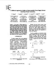
[4]. The proposed converter is shown in Fig. 1.<br />
c.<br />
c IQ<br />
do2<br />
II. - The proposed circuit.<br />
The circuit introduced in this paper was born from<br />
the application of the active Boost type <strong>clamping</strong> [2]<br />
to the <strong>new</strong> flyback-push-pull convertefll], generating<br />
a robust and efficient circuit.<br />
The <strong>new</strong> circuit is robust due to its immunity<br />
against leakage inductance variations in the two<br />
transformers connected in series. These inductances<br />
are included, in the case of the push-pull transformer,<br />
to the commutation process and in the case of the<br />
flyback transformer, to the energy transfer process.<br />
0-7803-5624-1/99/$10.00 0 1999 IEEE<br />
Fig. I - New converter a) <strong>non</strong>-coupled version and b)<br />
version with coupled input and output inductors.<br />
111, - Principle of operation.<br />
The main waveforms of the converter are shown in<br />
the Fig 2. In Fig. 2(a) and 2(b) the gating signals of<br />
the main and auxiliary switches are shown. Fig. 2(c)<br />
shows the current through the main switch (IS,&, the<br />
output diodes (a) and the auxiliary switch of the<br />
same pole (dashed line). Fig. 2(d) shows the current<br />
through the accumulation capacitor and finally, Fig.
2(e) shows the input current (iLlp). The converter<br />
has a total of ten stages for an operation cycle,<br />
however it is necessary to describe only five, i.e. for<br />
half period, since in the other portion of the period<br />
the operation is analogous.<br />
P Stage (G't,) Clamping capacitor's linear<br />
charge.<br />
At instant t=b, A gate-drive signal is applied to SIP<br />
and S,, while its body diodes are conducting,<br />
therefore they will commute without losses. In this<br />
stage the current in bp begins to increase and the<br />
source vi supplies energy to the accumulative<br />
capacitor Ca and to the load.<br />
A current flow in both transformers' primary<br />
windings yielding that a1 and a2 turns on and the<br />
output current starts to free wheel. At t=t, the current<br />
in the winding LZp reaches zero. The diode dlp is<br />
reverse biased and the switch SIP turns on, while the<br />
current through C, decreases.<br />
P Stage (t,-td Energy transfer.<br />
At t=tl iLIp it reaches its maximum value and the<br />
current through the capacitor C, reaches zero and<br />
inverts its direction. In this stage, energy is<br />
transferred from the source and of the capacitor C;,<br />
for the load. The commutation inductance and<br />
leakage inductance of the push-pull transformer are<br />
negligible in this stage due to that its currents are<br />
almost constant and only the input inductance L, (that<br />
is the flyback transformer leakage inductance) will<br />
have influence, due to its larger value.<br />
4 Stage (t&,) The first commutation.<br />
At t=b SIP is turns off, triggering the first process<br />
of lineal commutation. The capacitor CIpassumes the<br />
current allowing soft commutation in the switch. Note<br />
that the leakage inductance is used in the<br />
commutation. Due to the polarity of the current in LW<br />
and in LZp, the diode dol will be blocked and the<br />
conduction of the diode do2 will be reinforced in the<br />
output circuit.<br />
Q Stage<br />
discharge.<br />
Clamping capacitor's linear<br />
At t=f3 the voltage across Clp reaches VJ(1-D)<br />
causing dla to turn on, a portion of energy stored in<br />
the input inductance, as well as, of energy of the<br />
source are stored in it. The switch SI, can be gating<br />
under zero voltage. The currents through the<br />
inductance LdZp and LdW are constant, and therefore,<br />
they do not influence this stage.<br />
20- 1<br />
111. - Transfer Characteristic for<br />
D
20-1<br />
C. R. C. R.<br />
Fig. 3 - First stage.<br />
Fig. 7 - Fi’h<br />
stage.<br />
In the former expression, the gain of the converter<br />
is a function of the input current ripple, thus not being<br />
a good representation. Therefore, the connection is<br />
sought between this ripple and the output current.<br />
The input current ripple is given by:<br />
C.<br />
R.<br />
AI=(Vl+N V,,) D T-D T (Vl+N V,)<br />
4i (2 6 -1) 41 (2 6-1)<br />
Knowing that:<br />
- N .V,<br />
e v, =-<br />
Fig. 4 -Second stage. 77 v, V,.T.N v,<br />
-<br />
I, -vo 10 , I, =kL<br />
(4)<br />
(5)<br />
The normalized input current ripple is obtained as<br />
a function of the gain, the duty cycle and the<br />
normalized output current, as shown in the following<br />
equation:<br />
C.<br />
Fig. 5 - Third stage<br />
(2.6 -1) (1+6).q .d.(C +1)<br />
(6)<br />
Substituting the previous expression in the gain<br />
equation, given in (3), the normalized gain is<br />
obtained:<br />
Fig. 6 - Fourth stage.<br />
IV. - Design Methodology.<br />
Following a design procedure is proposed,<br />
switching supply based on the <strong>new</strong> converter.<br />
a. - Specifications<br />
These general specifications are:<br />
V, input Voltage<br />
Vo output Voltage<br />
Po output, Power<br />
F, commutation Frequency<br />
77 Efficiency<br />
D Dutycycle<br />
for a
20- 1<br />
6 Ratio between Li and Ld.<br />
The latter specification is very important because it<br />
furnishes a notion of the input current ripple. For<br />
continuous current, 5 >1 is necessary. However this<br />
value cannot be excessive ( 6 >50) since if the use of<br />
the proper leakage of the transformer flyback is<br />
requested, large values will imply in the use of a very<br />
volumous core. Therefore, an acceptable value (for<br />
acceptable cores) it is 10
20- 1<br />
integrated (IRF2111) is Tm=700ns, hence is<br />
assumed At6 = 100ns.<br />
The commercial value used was 15nF.<br />
lb. - Experimental Results.<br />
The power and control circuits of the experimental<br />
prototype are shown in Fig. 8a and Fig. 8b<br />
respectively. Four switches two transformers and<br />
two diocles constitute the power circuit. The <strong>isolated</strong><br />
command of the switches of the same leg is obtained<br />
through the IRF2111 integrated circuit.<br />
The experimental results were obtained at rated<br />
load power, which is equal to 600W.<br />
SIP, s7P9 SIA, s7A<br />
dol, do?<br />
Ds,,ds2 snubber output diodes<br />
Csl,Csl snubber output diodes<br />
Rsl,Rs2 snubber output diodes<br />
Output capacitor<br />
Ca Accumulation capacitor<br />
IRFP150<br />
MUR1530<br />
SKE 4W04<br />
4700pf 1.6KV<br />
polypropylene<br />
47KR 1/2W<br />
47uF 250V<br />
15uF 250V<br />
c.<br />
"I<br />
R.<br />
(b) Table N' 2: Control circuit.<br />
P4<br />
RI, R2<br />
R,. R,<br />
I Potentiometer de 1KQ<br />
Potentiometer de 10 KQ<br />
5,6KQ 1BW<br />
IS KO 1IRW<br />
Fig. 8 - Power (a) and control (6) diagrams<br />
Fig, 9 shows the currents in the primary (upper<br />
curve, IL,) and in the secondary winding (lower<br />
curve, IL,,) of the flyback transformer. Note that there<br />
is continuous current in the input and in the output,<br />
so the cclnverter is working as a DC-DC transformer.<br />
This means that there is no regeneration of the<br />
commutation and leakage inductance energy to the<br />
source. Instead, the energy is redirected to the load<br />
through the accumulation capacitor.<br />
This reduces the circulating reactive energy in the<br />
converter.
Fig. 9 - Flyback transformer currents ( lop s/div).<br />
Fig. 10 shows the voltages of the main and<br />
auxiliary MOSFET's; the effective <strong>clamping</strong> in the<br />
switches is clearly observed. The parasitic<br />
inductance of the circuit layout causes a voltage<br />
spike of approximately 22V. A possible solution for<br />
this situation is changing the position of the<br />
accumulation capacitor, placing it as near as possible<br />
of the switches.<br />
Fig. I I - Commutation process in the main switches atfull<br />
load. ( 5 p s/div).<br />
Fig. 12(a) shows the experimentally obtained<br />
efficiency of the circuit. It is observed that in 400W<br />
the efficiency starts to decrease; at full load (600W)<br />
the efficiency is 89.4 percent.<br />
Fig. 12(b) shows a comparison of the gain<br />
obtained experimentally (dot line) with that obtained<br />
theoretically.<br />
VDS<br />
0<br />
(b)<br />
Fig. 10 -Switch voltages: a) Main b) Auxiliary<br />
( 10 p s/div).<br />
Fig. 11 shows the commutation process in the<br />
main switches at full load, 600W. The <strong>new</strong> circuit<br />
seems quite robust, since it maintained soft switching<br />
with less than 1/5 of the nominal power.<br />
(b)<br />
Fig. 12 - (a) Experimental efJiciency as afunction of the<br />
output current. (b) Experimental gain.<br />
IV. - Conclusions<br />
In this paper a <strong>new</strong> current-fed capacitive<br />
accumulation converter was presented. The <strong>new</strong><br />
converter is capable of eliminating the problems of<br />
switch voltage overshoots due to the resonance<br />
between leakage inductance of the magnetic
20-1<br />
elements and the output capacitance of the<br />
MOSFETs.<br />
The proposed converter provides soft<br />
commutation (<strong>ZVS</strong>) in the switches and <strong>non</strong>pulsatinp<br />
input and output currents.<br />
The inductance's energy is used for the<br />
commutation of the switches and later on is<br />
accumulated in the accumulation capacitor and<br />
regenemted to the load, guaranteeing low reactive<br />
energy in the circuit. As a consequence of the<br />
transfer of energy with continuous current in the input<br />
as well as in the output, the. problems of the<br />
irradiated electromagnetic interference (EMI) are<br />
reduced.<br />
References<br />
[l] D.A. Ruiz-Caballero and I. Earbi, -A New Flyback -Current.<br />
Fed-PUSh..pull DC-DC Converter", IEEE IECON'98, pp 1036-1041,<br />
Aachen-Germany August 31- September 4,1998.<br />
[21 C.Duarte and I Earbi, 'A New Family of 2%-<strong>PWM</strong> Active<br />
Clamping DC-to-DC Boost Conveners: Analysis, Design and<br />
Experimentation' IEEE iNTELEC'96, pp. 305912 .<br />
[31 S. Cuk,"Switching DC-to-DC Converter with Zero input or<br />
Zero output Current Ripple" IEEE lnduslry Applications Society<br />
Annual Meeting. 1978 Record, pp. 1131-1146. Toronto , Ont..<br />
October 1..5. 1978.<br />
[4] G. Stoicic. D.M. Sable, F.C. Lee and E.H. Cho, "A <strong>new</strong><br />
Zero-Voltage Switching Weinberg Converter for High Voltage<br />
Space Power Distribuiton System", Pmceeding of the European<br />
Space Power Conference, Graz, Austria 23-24 August 1993.<br />
[5] D.A.Ruiz-Caballero, "A New Flyback-Push-Pull Current-Fed<br />
DC to DC Converter:ThmreticaI and ExDerimentai DeveloDrnent ",<br />
Ph.D. Thesis (in Portuguese). Federal University of Santa Catarina<br />
-Brazil (1999) Chapter 7.