
Create successful ePaper yourself
Turn your PDF publications into a flip-book with our unique Google optimized e-Paper software.
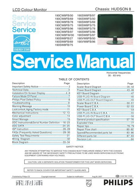
LCD Colour Monitor<br />
<strong>Service</strong><br />
<strong>Service</strong><br />
<strong>Service</strong><br />
190CW8FB/00<br />
190CW8FB/69<br />
190CW8FB/78<br />
190CW8FB/75<br />
190CW8FB/96<br />
190CW8FB/97<br />
190CW8FW/00<br />
190SW8FB/27<br />
190SW8FB/69<br />
190SW8FB/75<br />
190SW8FB/97<br />
190SW8FS/00<br />
190SW8FS/69<br />
190SW8FS/75<br />
190SW8FS/78<br />
190SW8FS/96<br />
190SW8FS/97<br />
190VW8FB/00<br />
190VW8FB/96<br />
Chassis: HUDSON 8<br />
Description<br />
Page<br />
Important Safety Notice---- ------------------------------ 2<br />
Technical Data----------------------------------------------3<br />
Instalation/On Screen Display------------------------4~6<br />
Failure Mode Of Panel ------------------------------------7<br />
Philips Pixel Defect Policy--------------------------------8<br />
Troubleshooting--------------------------------------------9<br />
Warning Message ----------------------------------------10<br />
Lock/unlock,Aging,Factory mode ---------------------11<br />
Mechanical Instructions----------------------------12~13<br />
Color adjustment -----------------------------------------14<br />
Smart Manage---------------------------------------------15<br />
DDC Instructions& Serial Number Definition ---16~23<br />
DDC DATA --------------------------------------------24~25<br />
ISP Instruction----------------------------------------26~28<br />
FAQs (Frequently Asked Questions) -------------29~30<br />
Safety Test Requirments--------------------------------31<br />
Wiring Diagram-------------------------------------------32<br />
Block Diagram----------------------------------------33~34<br />
TABLE OF CONTENTS<br />
SAFETY NOTICE<br />
Horizontal frequencies<br />
30-83kHz<br />
Description<br />
Page<br />
Scaler Board Diagram -----------------------------35~42<br />
Power Board Diagram -----------------------------43~46<br />
KEY Board Diagram-------------------------------------47<br />
USB-PLUG-IN Board Diagram------------------------48<br />
USB-PLUG-OUT Board Diagram---------------------49<br />
Scaler Board C.B.A.--------------------------------50~51<br />
Power Board C.B.A.--------------------------------52~53<br />
KEY Board C.B.A. ---------------------------------------54<br />
USB-PLUG-IN Board C.B.A. --------------------------55<br />
USB-PLUG-OUT Board C.B.A. -----------------------56<br />
General product specification--------------------57~76<br />
Exploded View -------------------------------------------77<br />
Repair tips--------------------------------------------78~79<br />
Repair Flow chart-----------------------------------80~82<br />
Spare&Recommended parts list-----------------83~86<br />
Different parts list-----------------------------------87~93<br />
Revision List----------------------------------------------94<br />
ANY PERSON ATTEMPTING TO SERVICE THIS CHASSIS MUST FAMILIARIZE HIMSELF WITH THE CHASSIS<br />
AND BE AWARE OF THE NECESSARY SAFETY PRECAUTIONS TO BE USED WHEN SERVICING ELECTRONIC<br />
EQUIPMENT CONTAINING HIGH VOLTAGES.<br />
CAUTION: USE A SEPARATE ISOLATION TRANSFORMER FOR THIS UNIT WHEN SERVICING.<br />
REFER TO BACK COVER FOR IMPORTANT SAFETY GUIDELINES<br />
Published by Philips CE Copyright reserved Subject to modification Aug,26, 2007<br />
GB 3122 785 17400
2 HUDSON 8<br />
Important Safety Notice<br />
Proper service and repair is important to the safe,<br />
reliable operation of all Philips Consumer Electronics<br />
Company** Equipment. The service procedures<br />
recommended by Philips and described in this service<br />
manual are effective methods of performing service<br />
operations. Some of these service operations require<br />
the use of tools specially designed for the purpose. The<br />
special tools should be used when and as<br />
recommended.<br />
It is important to note that this manual contains various<br />
CAUTIONS and NOTICES which should be carefully<br />
read in order to minimize the risk of personal injury to<br />
service personnel. The possibility exists that improper<br />
service methods may damage the equipment. It is also<br />
important to understand that these CAUTIONS and<br />
NOTICES ARE NOT EXHAUSTIVE. Philips could not<br />
possibly know, evaluate and advise the service trade of<br />
all conceivable ways in which service might be done or<br />
of the possible hazardous consequences of each way.<br />
Consequently, Philips has not undertaken any such<br />
broad evaluation. Accordingly, a servicer who uses a<br />
service procedure or tool which is not recommended by<br />
Philips must first satisfy himself thoroughly that neither<br />
his safety nor the safe operation of the equipment will<br />
be jeopardized by the service method selected.<br />
* * Hereafter throughout this manual, Philips Consumer<br />
Electronics Company will be referred to as Philips.<br />
WARNING<br />
Critical components having special safety<br />
characteristics are identified with a<br />
!<br />
by the Ref. No.<br />
in the parts list and enclosed within a broken line*<br />
(where several critical components are grouped in one<br />
area) along with the safety symbol<br />
!<br />
on the<br />
schematics or exploded views.<br />
Use of substitute replacement parts which do not have<br />
the same specified safety characteristics may create<br />
shock, fire, or other hazards.<br />
Take care during handling the LCD module with backlight<br />
unit<br />
- Must mount the moduleusing mounting holes arranged infour<br />
corners.<br />
- Do not press onthe panel, edge of theframe strongly or electric<br />
shock as this will result in damage to the screen.<br />
- Do not scratch orpress on the panel withany sharp objects, such<br />
as pencil or pen asthis may result in damage to the panel.<br />
- Protect the module fromthe ESD as it maydamage the electronic<br />
circuit (C-MOS).<br />
- Make certain that treatment person s body are grounded through<br />
wrist band.<br />
- Do not leave themodule in high temperature andin areas of high<br />
humidity for a long time.<br />
- Avoid contact with water as it may ashort circuit within the module.<br />
- If the surface ofpanel become dirty, please wipe it off with a soft<br />
material. (Cleaning with a dirty or rough cloth may damage the<br />
panel.)<br />
Under no circumstances should the original design be<br />
modified or altered without written permission from<br />
Philips. Philips assumes no liability, express or implied,<br />
arising out of any unauthorized modification of design.<br />
<strong>Service</strong>r assumes all liability.<br />
* Broken Line
Technical Data HUDSON 8<br />
3<br />
Type NR.<br />
Number of Pixels.<br />
: LPL, LM190WX1-TLA1 (TN)<br />
: 1440 (H) x900 (V)<br />
Pin Assignment<br />
Physical Size.<br />
: 427.2(H) x 277.4(V) x 15.3(D) mm(Typ.)<br />
Pixel Pitch.<br />
: 0.095*RGB(H)mm x 0.285(V)mm<br />
Color pixel arrangement. : RGB vertical stripes<br />
Support Color.<br />
: 16.7M colors<br />
Display Mode.<br />
: Normally White<br />
Backlight.<br />
: CCFL edge light system<br />
Pin No. Assignment<br />
Pin No.<br />
Active area. (WXH).<br />
: 410.4 (H) x 256.5 (V)<br />
Viewing Angle (CR>=10). : R/L 160(Typ.), U/D 160(Typ.)<br />
1 Red video input 9<br />
Contrast ratio.<br />
: 1000:1(Typ.) 700:1(Min.)<br />
2 Green video input<br />
10<br />
White luminance.<br />
: Original color 250 nits (Min),<br />
3 Blue video input 11<br />
300 nits (Typ.)<br />
4 GND<br />
12<br />
Type NR.<br />
: CMO, M190A1-L06 (TN)<br />
5 Cable detect<br />
13<br />
Number of Pixels.<br />
: 1440 (H) x900 (V)<br />
6 Red video GND<br />
Physical Size.<br />
: 427.2(w)277.4(h)17.0(d) (Typ) mm<br />
14<br />
Pixel Pitch.<br />
: 0.285 mm x 0.285 mm<br />
7 Green video GND 15<br />
Color pixel arrangement. : RGB vertical stripes<br />
Support Color. : 16.7M colors ( 6 bits+FRC )<br />
8<br />
Blue video GND<br />
Display Mode.<br />
: Normally White<br />
Backlight.<br />
: CCFL edge light system<br />
Input DVI-D connector pin<br />
Active area. (WXH).<br />
: 410.4 x 256.5mm (19.05”diagonal)<br />
Viewing Angle (CR>=10). : 75/75 (min), 85/85 (typ) for Horizontal &<br />
70/70 (min), 80/80 (typ) for Vertical<br />
Contrast ratio.<br />
: 850:1(Typ.) 500:1(Min.)<br />
White luminance.<br />
: Original color 230 nits (Min), 300 nits (Typ.)<br />
Assignment<br />
DDC +3.3V OR +5V<br />
GND<br />
GND<br />
Serial data line (SDA)<br />
H-sync<br />
V-sync<br />
Data clock line (SCL)<br />
Scanning frequencies<br />
H-Frequency.<br />
: 30K - 83 KHz<br />
V-Frequency.<br />
: 56 - 76 Hz<br />
Video dot rate.<br />
: < 140 MHz<br />
Power input.<br />
: 90-264 V AC, 50/60 2Hz<br />
Power consumption.<br />
: < 36W ( Typ.)<br />
Power Management Definition:<br />
STATUS H-sync V-sync Video Power LED<br />
On On On Active
4 HUDSON 8 Installation<br />
Front View<br />
USB Cable<br />
EDFU pack<br />
Connecting to Your PC<br />
1) Connect the power cord to the back of the monitor firmly. (Philips<br />
has pre-connected VGA cable for the first installation.<br />
I 1. To switch monitor's power On and Off<br />
OK<br />
2. MENU/ To access OSD menu<br />
3. To adjust the OSD<br />
4. To adjust brightness of the display<br />
5. AUTO/ Automatically adjust the horizontal position, vertical position,<br />
phase and clock settings / Return to previous OSD level.<br />
6. INPUT To change the signal input source.<br />
7. There are five modes to be selected: Office Work,<br />
Image Viewing, Entertainment, Economy, and Off.<br />
Rear View<br />
2) Connect to PC<br />
(a) Turn off your computer and unplug its power cable.<br />
(b) Connect the monitor signal cable to the video connector on the<br />
back of your computer.<br />
(c)<br />
(d)<br />
Plug the power cord of your computer and your monitor into a<br />
nearby outlet.<br />
Turn on your computer and monitor. If the monitor displays an<br />
image, installation is complete.<br />
The Base<br />
1 USB downstream port<br />
2 AC power input<br />
3 DVI-D input (Available for selected countries)<br />
4 VGA input<br />
5 USB upstream port<br />
6 Kensington anti-thief lock<br />
Attach and Detach the Base<br />
Attach the Base<br />
1) Place the base on flat surface, slide the monitor body onto the base.<br />
Accessory Pack<br />
Item<br />
Description<br />
Power cord<br />
VGA signal cable
Installation<br />
HUDSON 8<br />
5<br />
2) Install cable cover as illustrated below.<br />
Detach the Base<br />
Detach<br />
1) Remove the cable cover as illustrated below.<br />
2) Place the monitor face on a safe surface, push down on the<br />
release button and pull the base away from the monitor body.
6 HUDSON 8<br />
Go to cover page<br />
Description of the On Screen Display<br />
On Screen Display<br />
On-Screen Display (OSD) is a feature in all Philips LCD monitors. It allows an end user to adjust screen performance or select functions<br />
of the monitors directly through an on-screen instruction window. A user friendly on screen display interface is shown as below :<br />
Basic and simple instruction on the control keys.<br />
In the OSD shown above users can press buttons at the front bezel of the monitor to move the cursor, to confirm the choice or<br />
change,<br />
The OSD Tree<br />
Below is an overall view of the structure of the On-Screen Display. You can use this as a reference when you want to work your way around the<br />
different adjustments later on.
Failure Mode Of Panel<br />
HUDSON 8<br />
7<br />
Quick reference for failure mode of LCD panel<br />
this page presents problems that could be made by LCD panel.<br />
It is not necessary to repair circuit board. Simply follow the mechanical<br />
instruction on this manual to eliminate failure by replace LCD panel.<br />
Polarizer has bubbles<br />
Failure description<br />
Phenomenon<br />
Vertical block defect<br />
Polarizer has bubbles<br />
Vertical dim lines<br />
Foreign material inside<br />
polarizer. It shows liner or<br />
dot shape.<br />
Vertical lines defect<br />
(Always bright or dark)<br />
Concentric circle formed<br />
Horizontal block defect<br />
Bottom back light of LCD is<br />
brighter than normal<br />
Horizontal dim lines<br />
Back light un-uniformity<br />
Horizontal lines defect<br />
(Always bright or dark)<br />
Has bright or dark pixel<br />
Backlight has foreign material.<br />
Black or white color, liner or<br />
circular type
8 HUDSON 8 Philips Pixel Defect Policy<br />
Philips' Flat Panel Monitors Pixel Defect Policy<br />
Philips strives to deliver the highest quality products. We use some<br />
of the industry's most advanced manufacturing processes and<br />
practice stringent quality control. However, pixel or sub pixel<br />
defects on the TFT LCD panels used in flat panel monitors are<br />
sometimes unavoidable. No manufacturer can guarantee that all<br />
panels will be free from pixel defects, but Philips guarantees that<br />
any monitor with an unacceptable number of defects will be<br />
repaired or replaced under warranty. This notice explains the<br />
different types of pixel defects and defines acceptable defect<br />
levels for each type. In order to qualify for repair or replacement<br />
under warranty, the number of pixel defects on a TFT LCD panel<br />
must exceed these acceptable levels. For example, no more than<br />
0.0004% of the sub pixels on a 19"XGA monitor may be defective.<br />
Furthermore, Philips sets even higher quality standards for certain<br />
types or combinations of pixel defects that are more noticeable than<br />
others. This policy is valid worldwide.<br />
Proximity of Pixel Defects<br />
Because pixel and sub pixels defects of the same type that<br />
are near to one another may be more noticeable, Philips also<br />
specifies tolerances for the proximity of pixel defects.<br />
Pixel Defect Tolerances<br />
In order to qualify for repair or replacement due to pixel defects<br />
during the warranty period, a TFT LCD panel in a Philips flat<br />
panel monitor must have pixel or sub pixel defects exceeding the<br />
tolerances listed in the following tables.<br />
BRIGHT DOT DEFECTS<br />
ACCEPTABLE LEVEL<br />
MODEL 190SW8 190CW8<br />
1 lit subpixel 3orfewer 3orfewer<br />
2 adjacent lit subpixels 1 or fewer 1 or fewer<br />
Pixels and Sub pixels<br />
3 adjacent lit subpixels (one<br />
white pixel)<br />
Distance between two bright<br />
dot defects*<br />
Total bright dot defects of all<br />
types<br />
0 0<br />
15 mm or more 15 mm or more<br />
3orfewer 3orfewer<br />
A pixel, or picture element, is composed of three sub pixels<br />
in the primary colors of red, green and blue. Many pixels<br />
together form an image. When all sub pixels of a pixel are lit,<br />
the three colored sub pixels together appear as a single white<br />
pixel. When all are dark, the three colored sub pixels together<br />
appear as a single black pixel. Other combinations of lit and<br />
dark sub pixels appear as single pixels of other colors.<br />
Types of Pixel Defects<br />
Pixel and sub pixel defects appear on the screen in different ways.<br />
There are two categories of pixel defects and several types of sub<br />
pixel defects within each category.Bright Dot Defects Bright dot<br />
defects appear as pixels or sub pixels that are always lit or 'on'.<br />
That is,a bright dot is a sub-pixel that stands out on the screen<br />
when the monitor displays a dark pattern.There are the types<br />
of bright dot defects<br />
BLACK DOT DEFECTS<br />
ACCEPTABLE LEVEL<br />
MODEL 190SW8 190CW8<br />
1 dark subpixel 5orfewer 5orfewer<br />
2 adjacent dark subpixels 2 or fewer 2 or fewer<br />
3 adjacent dark subpixels 0 0<br />
Distance between two black<br />
dot defects*<br />
Total black dot defects of all<br />
types<br />
BLACK DOT DEFECTS<br />
15 mm or more 15 mm or more<br />
5orfewer<br />
5orfewer<br />
ACCEPTABLE LEVEL<br />
MODEL 190SW8 190CW8<br />
Total bright or black dot<br />
defects of all types<br />
5orfewer<br />
5orfewer<br />
Note:<br />
* 1 or 2 adjacent sub pixel defects = 1 dot defect<br />
All Philips monitors are ISO13406-2 Compliant<br />
Black Dot Defects Black dot defects appear as pixels or sub<br />
pixels that are always dark or 'off'. That is, a dark dot is a<br />
sub-pixel that stands out on the screen when the monitor<br />
displays a light pattern.These are the types of black dot defects:
Troubleshooting<br />
HUDSON 8<br />
9<br />
Common Problems<br />
Having this problem<br />
No Picture<br />
Power LED not lit)<br />
No Picture<br />
(Power LED is amber or yellow)<br />
Screen says<br />
Check these items<br />
Make sure the power cord is plugged into the power out let and<br />
into the back of the monitor.<br />
First, ensure that the power button on the front of the monitor is<br />
in the OFF position, then press it to the ON position.<br />
Make sure the computer is turned on.<br />
Make sure the signal cable is properly connected<br />
computer.<br />
Check to see if the monitor cable has bent pins.<br />
The Energy Saving feature may be activated<br />
Make sure the monitor cable is properly connected to<br />
your computer. (Also refer to the Quick Set-Up Guide).<br />
Check to see if the monitor cable has bent pins.<br />
Make sure the computer is turned on.<br />
AUTO button not working properly<br />
TheAutoFunctionisdesignedforuseonstandardMacintoshor<br />
IBM-compatible PCs running Microsoft Windows.<br />
It may not work properly if using nonstandard PC or videocard.<br />
Imaging Problems<br />
Display position is incorrect<br />
Image vibrates on the screen<br />
Vertical flicker appears<br />
Press the Auto button.<br />
Adjust the image position using the Phase/Clock of More Settings<br />
in OSD Main Controls.<br />
Check that the signal cable is properly connected to the<br />
graphics board or PC<br />
Press the Auto button.<br />
Eliminate the vertical bars using the Phase/Clock of More<br />
Settings in OSD Main Controls.<br />
Horizontal flicker appears<br />
Press the Auto button.<br />
Eliminate the vertical bars using the Phase/Clock of More<br />
Settings in OSD Main Controls.<br />
The screen is too bright or too dark<br />
An after-image appears<br />
An after-image remains after the power<br />
has been turned off.<br />
Green, red, blue, dark, and white dots<br />
Adjust the contrast and brightness on On-Screen Display.(The<br />
backlight of the LCD monitor has a fixed life span. When the screen<br />
becomes dark or begins to flicker, please contact your sales<br />
representative).<br />
If an image remains on the screen for an extended period of time,<br />
it may be imprinted in the screen and leave an afterimage.This<br />
usually disappears after a few hours<br />
This is characteristic of liquid crystal and is not caused by<br />
amalfunction or deterioration of the liquid crystal. The afterimage<br />
will disappear after a peroid of time.<br />
The remaining dots are normal characteristic of the liquid crystal
10 HUDSON 8 Warning Message<br />
Warning message table<br />
Item Attention Signals Display Time Condition<br />
1 CANNOT DISPLAY THIS 30 mins This warning appears when the input signal from your computer is not in<br />
VIDEO MODE, CHANGE<br />
a standard video mode or is out of the monitor s scanning range. After<br />
COMPUTER DISPLAY<br />
30 mins, monitor enters sleeping mode.<br />
INPUT TO 1280X1024 @<br />
60HZ<br />
2 NO VIDEO INPUT 30 mins This message appears when there is no signal input but with cable while<br />
AC or DC power on. After 30 mins, monitor enters sleeping mode.<br />
3 CHECK CABLE<br />
CONNECTION<br />
30 mins This message appears when a signal cable is disconnected while<br />
monitor is working. After 30 mins, monitor enters sleeping mode.<br />
4 ENTERING SLEEP MODE 3 secs This message appears when monitor is about to enter power saving<br />
mode.<br />
5 WAITING FOR AUTOMATIC<br />
ADJUSTMENT<br />
till auto adjustment<br />
finished<br />
This message is displayed when the auto adjustment button is pressed.<br />
It disappears when automatic adjustments are completed.<br />
6 USE 1280X 1024 FOR BEST<br />
RESULT<br />
On top of OSD main<br />
menu<br />
The message will show up at the top of the OSD main menu in red color<br />
when the input resolution is not the 1280x1024.<br />
7 OSD MAIN CONTROLS<br />
LOCKED<br />
3 secs / or Till "OSD<br />
MAIN CONTROLS<br />
UNLOCKED"<br />
appear<br />
This message will appear 3 seconds to indicate the OSD MAIN<br />
CONTROLS status when to lock or un-lock it by pressing "MENU(OK) "<br />
button for more than 10 seconds while there is video input from PC. This<br />
function provides the alternative that user can lock all the OSD main<br />
control in case user don t want the FOS performance setting to be<br />
changed, for instance, during commercial exhibition.<br />
8 OSD MAIN CONTROLS<br />
UNLOCKED<br />
3 secs This message will appear 3 seconds to indicate the OSD MAIN<br />
CONTROLS status when to un-lock it by pressing "MENU (OK) " button<br />
for more than 10 seconds while there is video input from PC.<br />
9 the window of "VOLUME" 60 secs This message will appear when the VOLUME button is pressed.<br />
10 THIS IS 85HZ OVERSCAN,<br />
CHANGE COMPUTER<br />
DISPLAY INPUT TO<br />
1280X1024@60HZ<br />
11 the window of OSD<br />
"MONITOR SETUP "<br />
12 the window of<br />
"BRIGHTNESS"<br />
13 "SELECTED INPUT NOT<br />
AVAILABLE"<br />
10 mins This message will appear 5 seconds in every 60 seconds for 10 minutes<br />
when the input of PC video timing is at 85Hz mode.<br />
Remark: AUTO is still functional in this mode<br />
60 secs This message will appear when the "OK" button is pressed.<br />
60 secs This message will appear when the BRIGHTNESS button is pressed.<br />
3 secs This message will appear 3 seconds to indicate the SIGNAL SOURCE<br />
status when change the signal source but it is not found while there is<br />
video input from PC.
Lock/Unlock,Aging,Factory Mode<br />
HUDSON 8<br />
11<br />
Front Control<br />
After 15 seconds,<br />
bring up:<br />
AGING...<br />
After 15 seconds,<br />
bring up:<br />
To Lock/Unlock OSD FUNCTION(User Mode)<br />
The OSD function can be locked by pressing"MENU"button for more<br />
than 10 seconds, the screen shows following windows for 4 seconds.<br />
Everytime when you press"MENU" button, this message<br />
appears on the screen automatically.<br />
----------<br />
----------<br />
repeatly<br />
Connect Signal cable again=> go back to normal display<br />
Access Factory Mode<br />
1). Turn off monitor.<br />
2). [Push "AUTO" & "MENU" buttons at the same time and hold them]<br />
+[Press "power" button untill comes out "Windows screen" ]<br />
=> then release all buttons<br />
3).Press "MENU" button, wait until the OSD menu with<br />
Characters "Factory" (below OSD menu) come on the Screen of<br />
the monitor.<br />
Unlock OSD function<br />
Unlocked OSD function can be released by pressing "MENU" button for<br />
more than 10 seconds again.<br />
Access Aging Mode<br />
Step1:Disconnect Interface Cable between Monitor and PC.<br />
Step 2 : Turn off LCD monitor.Then [Push "AUTO" & " MENU " buttons<br />
at the same time and hold them]+[Press power " " button untill comes<br />
out " AGING screen"] => then release all buttons.<br />
Bring up:<br />
AGING...<br />
Factory Mode indicator<br />
Enter Factory Menu<br />
Step1:Press"MENU"<br />
button.<br />
Step2:Choose" Picture ".<br />
Step3:Press" " button and choose" factory ".<br />
Step4:Press"MENU"<br />
button.<br />
After 15 seconds,<br />
bring up:
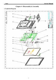
12 HUDSON 8 Mechanical Instruction<br />
Front View<br />
Fig.1<br />
Fig.6<br />
Back View<br />
5. Remove the 4 screws to remove the hinge ass'y as Fig.6.<br />
6. Remove the 1 screw as Fig.7.<br />
Step 1. Remove the Base.<br />
1. Remove the cable cover as Fig.3.<br />
2. Press the button as Fig.3 and pull out the base as Fig.4<br />
Fig.2<br />
Fig.7<br />
Fig.8<br />
Fig.3<br />
Step 2. Remove the Front bezel.<br />
1. Use plastic putty knife to release 6 snaps on the top side as Fig.8.<br />
2. Use plastic putty knife to release 4 snaps on the right side as Fig.9.<br />
3. Use plastic putty knife to release 4 snaps on the left side as Fig.10.<br />
Fig.4<br />
3. Remove the 3 screws to remove the Column as Fig.5.<br />
4. Remove the hinge cover as Fig.5.<br />
Fig.9<br />
Fig.5<br />
Fig.10
Mechanical Instruction<br />
HUDSON 8<br />
13<br />
4. Use plastic putty knife to release 6 snaps on the bottom side as Fig.11.<br />
5. Disconnect the cable of Key board as Fig.12.<br />
1. Remove the 5 screws to remove the shield as Fig.15.<br />
2. Remove the 6 screws and disconnect 8 calbe to remove the scaler<br />
board , power board and USB board as Fig.16.<br />
Fig.11<br />
Fig.16<br />
Fig.12<br />
Step 5. Remove the main frame.<br />
Remove the 4 screws as Fig.17.<br />
Step 3. Remove the Rear cover.<br />
Fig.17<br />
Fig.13<br />
Fig.18<br />
Fig.14<br />
1. Remove the 5 screws as Fig.13<br />
2. Disconnect the 1 cable of USB board as Fig.14<br />
Step 4. Remove the shield ., scaler board , power board and USB board.<br />
Fig.19<br />
Insulation material<br />
Fig.15
14 HUDSON 8 Color Adjustment<br />
Alignment procedure<br />
1. Turn on the LCD monitor.<br />
2.Turn on the Timing/pattern generator. See Fig.1<br />
3. Preset LCD color Analyzer CA-110<br />
-Remove the lens protective cover of probe CA-A30.<br />
-Set measuring/viewing selector to measuring position for reset<br />
analyzer.(zero calibration) as Fig.2<br />
- Turn on the color analyzer (CA-110)<br />
-Press 0-CAL button to starting reset analyzer.<br />
Measurement/viewing selector<br />
Fig.5<br />
Clear image<br />
Cover (black)<br />
5. Display<br />
Press “MENU”button to select. Change the value by "INPUT" or<br />
6. Display Adjustment<br />
key until the X,Y co-ordinates as below<br />
Measurement viewing selector<br />
Fig. 1 Fig. 2<br />
4. Access Factory Mode<br />
1). Turn off monitor.<br />
2). [Push "AUTO" & "MENU" buttons at the same time and hold them]<br />
+[Press "power" button untill comes out "Windows screen" ]<br />
=> then release all buttons<br />
3).Press "OK"<br />
button, wait until the OSD menu with Characters<br />
"Factory" (below OSD menu) come on the Screen of the monitor.<br />
as shown in Fig3.<br />
6.1 Auto color adjustment<br />
Apply a 1440*900/60Hz signal with 32 level grey pattern, set<br />
brightness control at 100%, and contrast control at 50%. Access to<br />
factory mode, and then press “Auto Level”to adjust RGB Gain and<br />
Offset. Check 64-grey pattern distinguishable.<br />
6.2 Adjustment of WHITE-D<br />
WD will be adjusted by FGA function automatically. When FGA is<br />
done successfully, the colour coordinate should be as follows with<br />
1440*900/60Hz signal and full white pattern:<br />
9300K<br />
6500K<br />
x (center) 0.283 0.005 0.313 0.005<br />
y (center) 0.297 0.005 0.329 0.005<br />
Use Minolta CA-210 for colour coordinates and luminance check.<br />
Luminance is > 300 Nits in the center of the screen when brightness<br />
at 100% and contrast set to 100%.<br />
6.2 Check of sRGB (B)<br />
Apply a 1440*900/ 60Hz signal with full white pattern, set brightness<br />
control at 100%, and contrast control at 50%. For the screen center,<br />
the 1931 CIE chromaticity Y) co-ordinates shall be:<br />
Factory Mode indicator Fig. 3<br />
4). Press "MENU" button, then select " factory " indicator by"INPUT"<br />
button .Press"MENU"<br />
button to bring up submenu windows as below:<br />
sRGB<br />
x(center) 0.313 0.005<br />
y(center) 0.329 0.005<br />
Y<br />
> 170 nits<br />
Fig. 4
Smart Manage<br />
HUDSON 8<br />
15<br />
2.Position<br />
Users can adjust the horizontal and vertical position of the screen<br />
by moving the sliding bar left and right. This function is disabled<br />
when using DVI-D (digit) input.<br />
Introduction<br />
Philips SmartManage is an advanced solution for users, corporate/<br />
institution IT administrator in particular, to manage their Philips<br />
monitors as part of the asset management environment. The<br />
solution includes three essential components, Philips SmartManage<br />
Administrator, and Philips SmarControl and Agent. Philips<br />
SmartManage is a solution joint developed by Philips and Altiris Inc.<br />
SmartManage Features and Benefits<br />
The Philips SmartManage is a working console for IT management<br />
to gather monitors assets information, run asset report, control<br />
assets security, monitor assets security, and issue instant messages<br />
to monitor users. Philips SmartManage includes the following major<br />
features:<br />
1. Provides an additional security measure that helps corporate<br />
users safeguard their<br />
investment.<br />
2. Power saving feature that reduces utility costs and manpower<br />
required to turn monitors on or off.<br />
3. SmartControl provides an efficient means for adjusting monitor<br />
performance and settings.<br />
4. Built-in asset reports reduce audit/maintenance manpower, cycle<br />
time and costs.<br />
A trial version of SmartManage can be downloaded from<br />
http://www.altiris.com/philips<br />
For more information of Philips SmartManage, please contact with<br />
Philips sales representatives in your country.<br />
Notes: SmartManage is a software dedicated to business<br />
environments. Personal users normally do not need to use<br />
SmartManage.<br />
Philips SmartControl<br />
The SmartControl and SmartManage Agent are deployed and<br />
installed in computers using Philips monitors. With SmartControl<br />
and SmartManage Agent, monitors and PCs can interact with the<br />
administrator's inquiries. Because SmartControl operates on<br />
individual PC, end users can also use SmartControl to adjust<br />
monitor's performance settings.<br />
1. Requirement<br />
1. Graphic cards with nVIDIA (TNT2, GeForce, Quadro, or newer)<br />
and ATI (Radeon or newer) graphic chipsets that support the<br />
DDC/CI interface<br />
2.Microsoft Windows 2000 and XP operation systems.<br />
3. Philips monitors supporting DDC/CI interface<br />
2. Installation<br />
How to download "SmartControl Installation " file:<br />
1. Visit http:// www.philips.com<br />
2. Select "Your Country"<br />
3. Click on "Support Center"<br />
4. Click into "Monitors and PC Products"<br />
5. Enter your model number<br />
6. Enter "Software" page<br />
7. Select "SmartControl Installation", and you can download<br />
SmartControl and its driver for installation.<br />
Please follow the guidance in the SmartControl installation program.<br />
3. Accessing SmartControl<br />
1. Right click on the desktop of your PC, and select Properties from<br />
the shortcut menu pops up.<br />
2. Click on Settings tab, and click on Advanced button.<br />
3. Click Philips SmartControl tab.<br />
4. SmartControl Options<br />
1.Display and Sound<br />
By moving the sliding bar toward left or right, users will be able<br />
to adjust brightness, contrast, audio volume (if applicable),<br />
video noise (not applicable when using DVI-D input), and color<br />
temperatures.<br />
3.Product Information<br />
Click Product Information in the left pane to view the product<br />
information stored in the monitor's memory.<br />
4.General<br />
Click on General for general information including driver<br />
information, device information, and monitor control.<br />
Within monitor control, users can click on Auto Setup to achieve<br />
optimum performance or click on factory reset to reset the<br />
parameters of the monitor. Such choices are disabled when using<br />
DVI-D(digit) input.
16 HUDSON 8 DDC Instructions<br />
General<br />
DDC Data Re-programming<br />
In case the DDC data memory IC or main EEPROM which storage all<br />
factory settings were replaced due to a defect, the serial numbers have<br />
to be re-programmed"Analog DDC IC, & EEPROM".<br />
It is advised to re-soldered DDC IC and main EEPROM from the old<br />
board onto the new board if circuit board have been replaced, in this case<br />
the DDC data does not need to be re-programmed.<br />
Additional information<br />
Additional information about DDC (Display Data Channel) may be<br />
obtained from Video Electronics Standards Association (VESA).<br />
Extended Display Identification Data(EDID) information may be also<br />
obtained from VESA.<br />
System and equipment requirements<br />
1. An i486 (or above) personal computer or compatible.<br />
2. Microsoft operation system Windows 95/98 .<br />
You have to Install the EDID_PORT_Tool under Win2000/XP . As<br />
Fig. 1 .<br />
Fig. 1<br />
A. Copy the "UserPort.sys" to C:\WINNT\system32\drivers(win2000)<br />
C:\WINDOWS\system32\drivers(winXP)<br />
B. Running " io.exe" everytime, Before you start to programming<br />
edid data .<br />
3. EDID45.exe program .<br />
4. DDC 2BI-ISP TOOL:<br />
Inclusion :<br />
A. DDC2BI-ISP TOOL(3138 106 10396) x1 (as Fig. 2)<br />
B. Printer cable x1<br />
c. (D-Sub) to (D-Sub) cable x2<br />
D. D-SUB to DVI cable X1<br />
Note: The EDID46.EXE is a windows-based program, which cannot<br />
be run in MS-DOS.<br />
Jumper at NORMAL To Printer positionport<br />
Jumper at VGA_5V position<br />
Jumper at VGA position<br />
Fig. 2<br />
Pin Assignment<br />
The digital only connector contains 24 signal contacts organized in<br />
three rows of eight contacts. Signal pin assignments are listed in the<br />
following table:<br />
To Printer port<br />
DC 8~12V<br />
DC 8~12V<br />
To Monitor<br />
D-sub/DVI cable<br />
To Monitor<br />
D-sub cable<br />
Power<br />
indicator<br />
PowerPin No.<br />
Description<br />
indicator<br />
1 T.M.D.S. data2-<br />
2 T.M.D.S. data2+<br />
3 T.M.D.S. data2 shield<br />
4 No Connect<br />
5 No Connect<br />
6 DDC clock<br />
7 DDC data<br />
8 No Connect<br />
9 T.M.D.S. data1-<br />
10 T.M.D.S. data1+<br />
11 T.M.D.S. data1 shield<br />
12 No Connect<br />
13 No Connect<br />
14 +5V Power<br />
15 Ground (for +5V) - Cable detect<br />
16 Hot plug detect<br />
17 T.M.D.S. data0-<br />
18 T.M.D.S. data0+<br />
19 T.M.D.S. data0 shield<br />
20 No Connect<br />
21 No Connect<br />
22 T.M.D.S clock shield<br />
23 T.M.D.S. clock+<br />
24 T.M.D.S. clock-<br />
Input analog D-sub connector pin assignment<br />
PIN No. SIGNAL<br />
1 Red video input<br />
2 Green video input / sync on green<br />
3 Blue video input<br />
4 GND<br />
5 GND--Cable detect<br />
6 Red video GND<br />
7 Green video GND<br />
8 Blue video GND<br />
9 DDC +3.3V or +5V<br />
10 Logic GND<br />
11 GND<br />
12 Serial data line (SDA)<br />
13 H-sync / H+V<br />
14 V-sync<br />
15 Data clock line (SCL)<br />
Fig. 3<br />
Fig. 4
DDC Instructions HUDSON 8<br />
17<br />
Configuration and procedure<br />
There is no Hardware DDC (DDC IC) anymore. Main EEPROM stores<br />
all factory settings and DDC data (EDID code) which is also called<br />
Software DDC. The following section describes the connection and<br />
procedure for Software DDC application. The main EEPROM can be reprogrammed<br />
by enabling '' factory memory data write'' function on the<br />
DDC program (EDID46.EXE).<br />
3. At the submenu, type the letter of your computer's hard disk drive<br />
followed by :EDID46 (for example, C:\EDID46, as shown in Fig. 6).<br />
Initialize alignment box<br />
In order to avoid that monitor entering power saving mode due<br />
to sync will cut off by alignment box, it is necessary to initialize<br />
alignment box before running programming software<br />
(EDID46.EXE). Following steps show you the procedures and<br />
connection.<br />
Step 1: Supply 8-12V DC power source to the Alignment box by<br />
plugging a DC power cord .<br />
Step 2: Connecting printer cable and D-Sub cable of monitor as Fig. 4<br />
1<br />
4. Click OK button. The main menu appears (as shown in Fig. 7).<br />
This is for initialize alignment box.<br />
Fig. 6<br />
PC<br />
1=Power connector<br />
2=D-SUB connector<br />
To printer port (LTP1)<br />
Step 3: Installation of EDID46.EXE<br />
DC Power<br />
8-12 V<br />
Printer<br />
Port<br />
To<br />
Monitor<br />
To PC<br />
Fig. 4<br />
Method 1: Start on DDC program<br />
Start Microsoft Windows.<br />
1. The Program"EDID46.EXE" in service manual cd-rom be copyed to C:\ .<br />
2. Click , choose Run at start menu of Windows as shown<br />
In Fig. 5.<br />
-----><br />
-----><br />
1 2<br />
Fig. 7<br />
Note 1: If the connection is improper, you will see the following error<br />
message (as shown in Fig. 8) before entering the main menu.<br />
Meanwhile, the (read EDID) function will be disable. At this<br />
time, please make sure all cables are connected correctly and<br />
fixedly, and the procedure has been performed properly.<br />
Fig. 8<br />
Fig. 5<br />
Note 2: During the loading, EDID46 will verify the EDID data which just<br />
loaded from monitor before proceed any further function, once<br />
the data structure of EDID can not be recognized, the following<br />
error message will appear on the screen as below. Please<br />
confirm following steps to avoid this message.<br />
1. The data structure of EDID was incorrect.<br />
2. DDC IC that you are trying to load data is empty.<br />
3. Wrong communication channel has set at configuration setup<br />
windows.<br />
4. Cables loosed or poor contact of connection.<br />
Fig. 9
18 HUDSON 8<br />
DDC Instructions<br />
Re-programming Analog DDC IC<br />
Step 1: After initialize alignment box, connecting all<br />
cables and box as shown in Fig. 10(unplug the 15th pin of<br />
the D-SUB cable connecting with monitor) .<br />
PC<br />
1=Power connector<br />
2=D-SUB connector<br />
To printer port (LTP1)<br />
DC Power<br />
8-12V<br />
Printer<br />
Port<br />
To<br />
Monitor<br />
To PC<br />
-----><br />
-----><br />
1 2<br />
Fig. 12<br />
3. Click OK button to confirm your selection.<br />
4. Click icon (Read EDID function) to read DDC EDID data from<br />
monitor. The EDID codes will display on screen as shown in Fig. 13.<br />
To PC Video port (D-sub)<br />
Fig. 13<br />
Unplug the 5th pin of D-SUB cable connecting with monitor<br />
Step 2: Read DDC data from monitor<br />
1. Click icon as shown in Fig. 11 from the tool bar to bring up<br />
the Channels "Configuration Setup" windows as shown in Fig. 11.<br />
Step 3: Modify DDC data (verify EDID version, week,<br />
year)<br />
Click (new function) icon from the tool bar, bring up<br />
Step 1 of 9 as shown in Fig. 14 .<br />
EDID46 DDC application provides the function selection and<br />
=====><br />
Click this button<br />
Fig. 11<br />
2. Select the DDC2Bi as the communication channel.<br />
As shown in Fig. 12.<br />
Fig. 14<br />
Select and fill out,<br />
If necessary.<br />
Fig. 14<br />
Step 4: Modify DDC data (Monitor Serial No.)<br />
1. Click Next , bring up Fig. 15.
DDC Instructions HUDSON 8<br />
19<br />
2. Click Next , bring up Fig.16.<br />
Fig. 15<br />
5. Click Next , bring up Fig.19.<br />
Fig. 18<br />
Fig. 19<br />
3. Click Next , bring up Fig.17.<br />
Fig. 16<br />
6. Click Next , bring up Fig. 20.<br />
In this step, please confirm the Descriptor Data Type is Monitor<br />
Range Limits, and all the items are same as below.<br />
4. Click Next , bring up Fig.18.<br />
Fig. 17<br />
NOTE: You must modify the Serial NO. In step 7, otherwise the<br />
Serial NO. In OSD Couldn't be modified correctly.<br />
Fig. 20
20 HUDSON 8<br />
DDC Instructions<br />
7. Click Next , bring up Fig. 21.<br />
8. Click Next , bring up Fig. 22, then click "finish".<br />
Fig. 21<br />
Fig. 24<br />
Step 6: Save DDC data<br />
Sometimes, you may need to save DDC data as a text file for<br />
using in other IC chip. To save DDC data, follow the steps below:<br />
1. Click (Save) icon (or click "file"-> "save as") from the tool bar<br />
and give a file name as shown in Fig. 25.<br />
The file type is EDID46 file (*.ddc) which can be open in WordPad.<br />
By using WordPad, the texts of DDC data & table (128 bytes, hex<br />
code) can be modified. If DDC TEXTS & HEX Table ar completely<br />
correct, it can be saved as .ddc flie to re-load it into DDC IC for DDC<br />
Data application.<br />
Step 5: Write DDC data<br />
1. Configuration should be as Fig. 23. And press OK.<br />
Fig. 22<br />
2. Click Save.<br />
Step 7: Exit DDC program<br />
Pull down the File menu and select Exit as shown in Fig. 26.<br />
Fig. 25<br />
Fig. 23<br />
Fig. 26<br />
2. Click (Write EDID) icon from the tool bar to write DDC data.<br />
Then wait for 20-30 seconds ,DDC data will be finished Writing.<br />
3. Turn off the monitor, press "INPUT" button and hold it , then press<br />
power button to turn on the monitor.(If the power indicator light flicker<br />
twice, it means the S/N has been refreshed into the EEPROM.)<br />
4 Press "MENU" button . The S/N is refreshed in the OSD menu as<br />
Fig.24.
DDC Instructions HUDSON 8<br />
21<br />
Re-programming Digital DDC IC<br />
Step 1: After initialize alignment box, connecting all<br />
cables and box as shown in Fig. 27(Unplug the 15th pin of<br />
The DVI cable connecting with monitor).<br />
3. Click OK button to confirm your selection.<br />
4. Click icon (Read EDID function) to read DDC EDID data from<br />
monitor. The EDID codes will display on screen as shown in Fig. 30.<br />
Monitor A<br />
PC<br />
Monitor B(190CW8)<br />
1=DVI-D connector<br />
2<br />
2=D-sub connector<br />
To video card<br />
To printer port (LTP1)<br />
Printer<br />
Port<br />
DC Power<br />
8 12V ~<br />
To<br />
Monitor<br />
3<br />
D-sub to DVI-D cable<br />
1<br />
D-sub cable<br />
Fig. 30<br />
Step 3: Modify DDC data (verify EDID version, week,<br />
year)<br />
Click (new function) icon from the tool bar, bring up<br />
Step 1 of 9 as shown in Fig. 31 .<br />
EDID46 DDC application provides the function selection and<br />
text change (select & fill out) from Step 1 to Step 9.<br />
Unplug the 15th pin of DVI cable connecting with monitor<br />
Fig. 27<br />
Step 2: Read DDC data from monitor<br />
1. Click icon as shown in Fig. 11 from the tool bar to bring up<br />
the Channels "Configuration Setup" windows as shown in Fig. 28.<br />
=====><br />
Click this button<br />
Select and fill out,<br />
If necessary.<br />
Fig. 31<br />
Fig. 28<br />
2. Select the DDC2Bi as the communication channel.<br />
As shown in Fig. 29.<br />
Fig. 29<br />
Fig. 32
22 HUDSON 8<br />
DDC Instructions<br />
Step 4: Modify DDC data (Monitor Serial No.)<br />
1. Click Next , bring up Fig. 32.<br />
2. Click Next , bring up Fig. 33.<br />
3. Click Next , bring up Fig. 34.<br />
Fig. 36<br />
6. Click Next , bring up Fig. 37.<br />
NOTE: You must modify the Serial NO. In step 7, otherwise<br />
the Serial NO. In OSD Couldn't be modified correctly.<br />
Fig. 33 7. Click Next , bring up Fig. 38.<br />
4. Click Next , bring up Fig. 35.<br />
5. Click Next , bring up Fig. 36.<br />
Fig. 34<br />
Fig. 37<br />
Fig. 35<br />
Fig. 38
DDC Instructions HUDSON 8<br />
23<br />
8. Click Next , bring up Fig. 39.<br />
In this step, please confirm the Descriptor Data Type is Monitor<br />
Range Limits, and all the items are same as below.<br />
2. Click Save.<br />
Step 7: Exit DDC program<br />
Pull down the File menu and select Exit as shown in Fig. 42.<br />
Fig.39<br />
Fig.42<br />
Step 8: Turn off the monitor, exit the factory mode.<br />
Serial Number Definition<br />
Step 5: Write DDC data<br />
1. Configuration should be as Fig. 40. And press OK.<br />
Fig.40<br />
2. Click (Write EDID) icon from the tool bar to write DDC data.<br />
Then wait for 20-30 seconds ,DDC data will be finished Writing.<br />
3. Turn off the monitor, press “INPUT”button and hold it , then press<br />
power button to turn on the monitor.(If the power indicator light flicker<br />
twice, it means the S/N has been refreshed into the EEPROM.)<br />
Step 6: Save DDC data<br />
Sometimes, you may need to save DDC data as a text file for using in<br />
other IC chip. To save DDC data, follow the steps below:<br />
1. Click (Save) icon (or click "file"-> "save as") from the tool bar<br />
and give a file name as shown in Fig. 41.<br />
ThefiletypeisEDID46file(*.ddc)whichcanbeopeninWordPad.<br />
By using WordPad, the texts of DDC data & table (128 bytes, hex code)<br />
can be modified. If DDC TEXTS & HEX Table ar completely correct, it<br />
can be saved as *.ddc flie to re-load it into DDC IC for DDC Data<br />
application.<br />
BOM Code<br />
Panel Supplier CODE<br />
AUO 1<br />
CPT 2<br />
LPL(LG) 3<br />
QDI 4<br />
CMO 5<br />
BZ1A0625000001<br />
SERIAL NO<br />
YEAR/WEEK<br />
SERVICE VERSION CHANGE CODE<br />
BOM CODE(BILL OF MATERIAL)CODE<br />
SITE CODE(PRODUCTION CENTER)<br />
BZ CODE(AR-CZECH REPUBLIC<br />
VN-HUNGARY(SZR),BZ-SUZHOU<br />
DS-DONGGUAN)<br />
Fig.41
24 HUDSON 8 DDC DATA<br />
For 190CW8 CMO panel (analog DDC)<br />
**********************************************************************<br />
EDID log file<br />
**********************************************************************<br />
Vendor/Product Identification<br />
ID Manufacturer Name : PHL<br />
ID Product Code<br />
: C018 (HEX.)<br />
ID Serial Number<br />
: 4F536 (HEX.)<br />
Week of Manufacture : 35<br />
Year of Manufacture : 2007<br />
EDID Version, Revision<br />
Version : 1<br />
Revision : 3<br />
Basic Display Parameters/Features<br />
Video Input Definition : Analog Video Input<br />
0.700V/0.300V (1.00Vpp)<br />
without Blank-to-Black Setup<br />
Separate Sync<br />
Composite Sync<br />
Sync on Green<br />
no Serration required<br />
Maximum H Image Size : 40<br />
Maximum V Image Size : 25<br />
Display Transfer Characteristic : 2.2<br />
(gamma)<br />
Feature Support (DPMS)<br />
no Suspend<br />
Active Off<br />
: no Standby<br />
Display Type<br />
: RGB color display<br />
Preferred Timing Mode : Detailed timing block 1<br />
Color Characteristics<br />
Red X coordinate : 0.639<br />
Red Y coordinate : 0.342<br />
Green X coordinate : 0.297<br />
Green Y coordinate : 0.614<br />
Blue X coordinate : 0.146<br />
Blue Y coordinate : 0.067<br />
White X coordinate : 0.313<br />
White Y coordinate : 0.328<br />
Established Timings<br />
Established Timings I<br />
Established Timings II<br />
Manufacturer's timings<br />
Standard Timing Identification #1<br />
Horizontal active pixels : 1152<br />
Aspect Ratio : 4:3<br />
Refresh Rate : 75<br />
: 720 x 400 @70Hz (IBM,VGA)<br />
640 x 480 @60Hz (IBM,VGA)<br />
640 x 480 @67Hz (Apple,Mac II)<br />
640 x 480 @72Hz (VESA)<br />
640 x 480 @75Hz (VESA)<br />
800 x 600 @56Hz (VESA)<br />
800 x 600 @60Hz (VESA)<br />
: 800 x 600 @72Hz (VESA)<br />
800 x 600 @75Hz (VESA)<br />
832 x 624 @75Hz (Apple,Mac II)<br />
1024 x 768 @60Hz (VESA)<br />
1024 x 768 @70Hz (VESA)<br />
1024 x 768 @75Hz (VESA)<br />
: 1152 x 870 @75Hz (Apple,Mac II)<br />
Standard Timing Identification #3<br />
Horizontal active pixels : 1440<br />
Aspect Ratio : 16:10<br />
Refresh Rate : 75<br />
Detailed Timing #1<br />
Pixel Clock (MHz) : 106.5<br />
H Active (pixels) : 1440<br />
H Blanking (pixels) : 464<br />
V Active (lines) : 900<br />
V Blanking (lines) : 34<br />
H Sync Offset (F Porch) (pixels): 80<br />
H Sync Pulse Width (pixels) : 152<br />
V Sync Offset (F Porch) (lines) : 3<br />
V Sync Pulse Width (lines) : 6<br />
H Image Size (mm) : 408<br />
V Image Size (mm) : 255<br />
H Border (pixels) : 0<br />
V Border (lines) : 0<br />
Flags<br />
: Non-interlaced<br />
: Normal Display, No stereo<br />
: Digital Separate sync.<br />
: Positive Vertical Sync.<br />
: Negative Horizontal Sync.<br />
Monitor Descriptor #2<br />
Serial Number<br />
Monitor Descriptor #3<br />
Monitor Name<br />
: BZ10735324918<br />
: Philips 190CW<br />
Monitor Descriptor #4<br />
Monitor Range Limits<br />
Min. Vt rate Hz : 56<br />
Max. Vt rate Hz : 76<br />
Min. Horiz. rate kHz : 30<br />
Max. Horiz. rate kHz : 83<br />
Max. Supported Pixel : 140<br />
No secondary GTF timing formula supported.<br />
Extension Flag : 0<br />
Check sum<br />
: A7 (HEX.)<br />
**********************************************************************<br />
EDID data (128 bytes)<br />
**********************************************************************<br />
0: 00 1: ff 2: ff 3: ff 4: ff 5: ff 6: ff 7: 00<br />
8: 41 9: 0c 10: 18 11: c0 12: 36 13: f5 14: 04 15: 00<br />
16: 23 17: 11 18: 01 19: 03 20: 0e 21: 28 22: 19 23: 78<br />
24: 2a 25: a1 26: 50 27: a3 28: 57 29: 4c 30: 9d 31: 25<br />
32: 11 33: 50 34: 54 35: bf 36: ee 37: 80 38: 71 39: 4f<br />
40: 95 41: 00 42: 95 43: 0f 44: 01 45: 01 46: 01 47: 01<br />
48: 01 49: 01 50: 01 51: 01 52: 01 53: 01 54: 9a 55: 29<br />
56: a0 57: d0 58: 51 59: 84 60: 22 61: 30 62: 50 63: 98<br />
64: 36 65: 00 66: 98 67: ff 68: 10 69: 00 70: 00 71: 1c<br />
72: 00 73: 00 74: 00 75: ff 76: 00 77: 42 78: 5a 79: 31<br />
80: 30 81: 37 82: 33 83: 35 84: 33 85: 32 86: 34 87: 39<br />
88: 31 89: 38 90: 00 91: 00 92: 00 93: fc 94: 00 95: 50<br />
96: 68 97: 69 98: 6c 99: 69 100: 70 101: 73 102: 20 103: 31<br />
104: 39 105: 30 106: 43 107: 57 108: 00 109: 00 110: 00 111: fd<br />
112: 00 113: 38 114: 4c 115: 1e 116: 53 117: 0e 118: 00 119: 0a<br />
120: 20 121: 20 122: 20 123: 20 124: 20 125: 20 126: 00 127: a7<br />
Standard Timing Identification #2<br />
Horizontal active pixels : 1440<br />
Aspect Ratio : 16:10<br />
Refresh Rate : 60
DDC DATA HUDSON 8<br />
25<br />
For 190CW8 CMO panel (digital DDC)<br />
**********************************************************************<br />
EDID log file<br />
**********************************************************************<br />
Vendor/Product Identification<br />
ID Manufacturer Name : PHL<br />
ID Product Code : C018 (HEX.)<br />
ID Serial Number : 4F536 (HEX.)<br />
Week of Manufacture : 35<br />
Year of Manufacture : 2007<br />
EDID Version, Revision<br />
Version : 1<br />
Revision : 3<br />
Basic Display Parameters/Features<br />
Video Input Definition : Digital Video Input<br />
Maximum H Image Size : 40<br />
Maximum V Image Size : 25<br />
Display Transfer Characteristic : 2.2<br />
(gamma)<br />
Feature Support (DPMS) : no Standby<br />
no Suspend<br />
Active Off<br />
Display Type : RGB color display<br />
Preferred Timing Mode : Detailed timing block 1<br />
Color Characteristics<br />
Red X coordinate : 0.639<br />
Red Y coordinate : 0.342<br />
Green X coordinate : 0.297<br />
Green Y coordinate : 0.614<br />
Blue X coordinate : 0.146<br />
Blue Y coordinate : 0.067<br />
White X coordinate : 0.313<br />
White Y coordinate : 0.328<br />
Established Timings<br />
Established Timings I : 720 x 400 @70Hz (IBM,VGA)<br />
640 x 480 @60Hz (IBM,VGA)<br />
640 x 480 @67Hz (Apple,Mac II)<br />
640 x 480 @72Hz (VESA)<br />
640 x 480 @75Hz (VESA)<br />
800 x 600 @56Hz (VESA)<br />
800 x 600 @60Hz (VESA)<br />
Established Timings II : 800 x 600 @72Hz (VESA)<br />
800 x 600 @75Hz (VESA)<br />
832 x 624 @75Hz (Apple,Mac II)<br />
1024 x 768 @60Hz (VESA)<br />
1024 x 768 @70Hz (VESA)<br />
1024 x 768 @75Hz (VESA)<br />
Manufacturer's timings : 1152 x 870 @75Hz (Apple,Mac II)<br />
Standard Timing Identification #1<br />
Horizontal active pixels : 1152<br />
Aspect Ratio : 4:3<br />
Refresh Rate : 75<br />
Detailed Timing #1<br />
Pixel Clock (MHz) : 106.5<br />
H Active (pixels) : 1440<br />
H Blanking (pixels) : 464<br />
V Active (lines) : 900<br />
V Blanking (lines) : 34<br />
H Sync Offset (F Porch) (pixels) : 80<br />
H Sync Pulse Width (pixels) : 152<br />
VSyncOffset(FPorch)(lines) : 3<br />
V Sync Pulse Width (lines) : 6<br />
H Image Size (mm) : 408<br />
V Image Size (mm) : 255<br />
H Border (pixels) : 0<br />
V Border (lines) : 0<br />
Flags : Non-interlaced<br />
: Normal Display, No stereo<br />
: Digital Separate sync.<br />
: Positive Vertical Sync.<br />
: Negative Horizontal Sync.<br />
Monitor Descriptor #2<br />
Serial Number : BZ10735324918<br />
Monitor Descriptor #3<br />
Monitor Name : Philips 190CW<br />
Monitor Descriptor #4<br />
Monitor Range Limits<br />
Min.VtrateHz : 56<br />
Max. Vt rate Hz : 76<br />
Min. Horiz. rate kHz : 30<br />
Max. Horiz. rate kHz : 83<br />
Max. Supported Pixel : 140<br />
No secondary GTF timing formula supported.<br />
Extension Flag : 0<br />
Check sum : 35 (HEX.)<br />
**********************************************************************<br />
EDID data (128 bytes)<br />
**********************************************************************<br />
0: 00 1: ff 2: ff 3: ff 4: ff 5: ff 6: ff 7: 00<br />
8: 41 9: 0c 10: 18 11: c0 12: 36 13: f5 14: 04 15: 00<br />
16: 23 17: 11 18: 01 19: 03 20: 80 21: 28 22: 19 23: 78<br />
24: 2a 25: a1 26: 50 27: a3 28: 57 29: 4c 30: 9d 31: 25<br />
32: 11 33: 50 34: 54 35: bf 36: ee 37: 80 38: 71 39: 4f<br />
40: 95 41: 00 42: 95 43: 0f 44: 01 45: 01 46: 01 47: 01<br />
48: 01 49: 01 50: 01 51: 01 52: 01 53: 01 54: 9a 55: 29<br />
56: a0 57: d0 58: 51 59: 84 60: 22 61: 30 62: 50 63: 98<br />
64: 36 65: 00 66: 98 67: ff 68: 10 69: 00 70: 00 71: 1c<br />
72: 00 73: 00 74: 00 75: ff 76: 00 77: 42 78: 5a 79: 31<br />
80: 30 81: 37 82: 33 83: 35 84: 33 85: 32 86: 34 87: 39<br />
88: 31 89: 38 90: 00 91: 00 92: 00 93: fc 94: 00 95: 50<br />
96: 68 97: 69 98: 6c 99: 69 100: 70 101: 73 102: 20 103: 31<br />
104: 39 105: 30 106: 43 107: 57 108: 00 109: 00 110: 00 111: fd<br />
112: 00 113: 38 114: 4c 115: 1e 116: 53 117: 0e 118: 00 119: 0a<br />
120: 20 121: 20 122: 20 123: 20 124: 20 125: 20 126: 00 127: 35<br />
Standard Timing Identification #2<br />
Horizontal active pixels : 1440<br />
Aspect Ratio : 16:10<br />
Refresh Rate : 60<br />
Standard Timing Identification #3<br />
Horizontal active pixels : 1440<br />
Aspect Ratio : 16:10<br />
Refresh Rate : 75
26 HUDSON 8 ISP Instructions<br />
Step 1. Save the MST ISP tool to your computer.<br />
ISP_TOOL V4.2.0 TPV (958KB,Created day: 2007.01.26)<br />
ISP_TOOL V4.2.0 TPV<br />
2. Save the BIN files(hexcode) to your computer,<br />
Step 2: Connect to ISP Board,P/N:3138 106 10396.<br />
Connect to PC Printing port<br />
Connect to monitor D-SUB<br />
Jumper at the VGA position<br />
Jumper at the VGA-5V position<br />
Jumper at the NORMAL position<br />
Step 3: Update TV.<br />
I. Open the ISP_TOOL V4.2.0 TPV.EXE
ISP Instruction HUDSON 8<br />
27<br />
2. Click "Dis Con"<br />
3. Click "connect",<br />
4. Click "Device" to choose the device type Pm25LV010(A).<br />
5. Click "Load" to choose the corresponding ISP software according the model. .
28 HUDSON 8 ISP Instruction<br />
6. Click "Read", then click "Read" to choose the corresponding ISP software according the model.<br />
Then click "Auto", and run it until OK.
FAQs (Frequently Asked Questions)<br />
HUDSON 8<br />
29<br />
General FAQs<br />
Q: When I install my monitor what should I do if the screen shows 'Cannot display this video mode'?<br />
A: Recommended video mode for Philips 19": 1440x900 @60Hz.<br />
1. Unplug all cables, then connect your PC to the monitor that you used previously.<br />
2. In the Windows Start Menu, select Settings/Control Panel. In the Control Panel Window, select the Display icon. Inside the Display<br />
Control Panel, select the 'Settings' tab. Under the setting tab, in box labeled 'desktop area', move the slidebar to 1440x900 pixels (19").<br />
3. Open 'Advanced Properties' and set the Refresh Rate to 60Hz, then click OK.<br />
4. Restart your computer and repeat step 2 and 3 to verify that your PC is set at 1440x900@60Hz (19").<br />
5. Shut down your computer, disconnect your old monitor and reconnect your Philips LCD monitor.<br />
6. Turn on your monitor and then turn on your PC.<br />
Q: What does 'refresh rate' mean in connection with an LCD monitor?<br />
A:The refresh rate is of much less relevance for LCD monitors. LCD monitors display a stable, flicker-free image at 60Hz.<br />
There is no visible difference between 85Hz and 60Hz.<br />
Q: What are the .inf and .icm files on the CD-ROM? How do I install the drivers (.inf and .<br />
icm)?<br />
A:These are the driver files for your monitor. Follow the instructions in your user manual to install the drivers. Your computer may ask you for<br />
monitor drivers (.inf and .icm files) or a driver disk when you first install your monitor. Follow the instructions to Insert the ( companion CD-ROM)<br />
included in this package. Monitor drivers (.inf and .icm files) will be installed automatically.<br />
Q: How do I adjust the resolution?<br />
A:Your video card/graphic driver and monitor together determine the available resolutions. You can select the desired resolution under Windows®<br />
Control Panel with the "Display properties"<br />
Q: What if I get lost when I am making monitor adjustments?<br />
A: Simply press the OK button, then select 'Reset' to recall all of the original factory settings.<br />
Q: What is the Auto function?<br />
A:The AUTO adjustment key restores the optimal screen position, phase and clock settings by pressing of a single button – without the need to<br />
navigate through OSD (On Screen Display) menus and control keys.<br />
Note:Autofunctionisavailableinselectedmodelsonly.<br />
Q: My Monitor has no power (Power LED does not light up). What should I do?<br />
A: Make sure the AC power cord is connected between the monitor and AC outlet,and click a key on keyboard/mouse to wake up the PC.<br />
Q: Will the LCD monitor accept an interlaced signal under PC models?<br />
A: No. If an Interlace signal is used, the screen displays both odd and even horizontal scanning lines at the same time, thus distorting the picture.<br />
Q:What does the Refresh Rate mean for LCD?<br />
A: Unlike CRT display technology, in which the speed of the electron beam is swept from the top to the bottom of the screen determines flicker,<br />
an active matrix display uses an active element (TFT) to control each individual pixel and the refresh rate is therefore not really applicable to<br />
LCD technology.<br />
Q: Will the LCD screen be resistant to scratches?<br />
A: A protective coating is applied to the surface of the LCD, which is durable to a certain extent (approximately up to the hardness of a 2H pencil).<br />
In general, it is recommended that the panel surface is not subject to any excessive shocks or scratches.<br />
Q: How should I clean the LCD surface?<br />
A: For normal cleaning, use a clean, soft cloth. For extensive cleaning, please use isopropyl alcohol. Do not use other solvents such as ethyl<br />
alcohol, ethanol, acetone, hexane, etc<br />
.<br />
Q:Can I change the color setting of my monitor?<br />
A:Yes, you can change your color setting through OSD control as the followingprocedures,<br />
1. Press "OK" to show the OSD (On Screen Display) menu<br />
2. Press "Down Arrow" to select the option "Color" then press "OK" to enter colorsetting, there are four settings as below.<br />
a. Color Temperature; The six settings are 5000K, 6500K, 7500K, 8200K, 9300K and 11500K. With settings in the 5000K range the panel<br />
appears<br />
'warm', with a red-white color tone, while a 11500K temperature yields 'cool,blue-white toning."<br />
b. sRGB; this is a standard setting for ensuring correct exchange of colors between different device (e.g. digital cameras, monitors, printers,<br />
scanners,etc)<br />
c. User Define; the user can choose his/her preference color setting by adjusting red, green blue color.<br />
*A measurement of the color of light radiated by an object while it is being heated.This measurement is expressed in terms of absolute scale,<br />
(degrees Kelvin). Lower Kevin temperatures such as 2004K are red; higher temperatures such as 9300K are blue. Neutral temperature is<br />
white, at 6504K.<br />
Q: Can the Philips LCD Monitor be mounted on the wall?<br />
A: Yes. Philips LCD monitors have this optional feature. For standard VESA mount holes on the rear cover allows the user to mount the Philips<br />
monitor on most of the VESA standard arms or accessories. We recommend to contact your Philips sales representative for more information.<br />
Screen Adjustments<br />
Q: When I install my monitor, how do I get the best performance from the monitor?<br />
A:For best performance, make sure your display settings are set at 1440x900@60Hz for 19". Note: You can check the current display<br />
settings by pressing the OSD OK button once. The current display mode is shown in OSD first page.
30 HUDSON 8 FAQs (Frequently Asked Questions)<br />
Q: How do LCDs compare to CRTs in terms of radiation?<br />
A: Because LCDs do not use an electron gun, they do not generate the same amount of radiation at the screen surface.<br />
Compatibility with other Peripherals<br />
Q: Can I connect my LCD monitor to any PC, workstation or Mac?<br />
A: Yes. All Philips LCD monitors are fully compatible with standard PCs, Macs and workstations. You may need a cable adapter to connect the<br />
monitor to your Mac system. Please contact your Philips sales representative for more information.<br />
Q: Are Philips LCD monitors Plug-and-Play?<br />
A: Yes, the monitors are Plug-and-Play compatible with Windows® 95, 98, 2000, XP and Vista<br />
Q: What is USB (Universal Serial Bus)?<br />
A: Think of USB as a smart plug for PC peripherals. USB automatically determinesresources (like driver software and bus bandwidth) required by<br />
peripherals. USB makes necessary resources available without user intervention. There are three main benefits of USB. USB eliminates "case<br />
anxiety," the fear of removing the computer case to install circuit board cards -- that often requires adjustment of complicated IRQ settings -- for<br />
add-on peripherals. USB does away with "port gridlock." Without USB, PCs are normally limited to one printer, two Com port devices (usually a<br />
mouse and modem), one Enhanced Parallel Port add-on (scanner or video camera, for example),and a joystick. More and more peripherals for<br />
multimedia computers come on the market every day. With USB, up to 127 devices can run simultaneously on one computer. USB permits "hot<br />
plug-in." No need to shut down, plug in, reboot and run set up to install peripherals. No need to go through the reverse process to unplug a<br />
device. Bottom line: USB transforms today's "Plug-and-Pray" into true Plug-and-Play!Please refer to glossary for more information about USB.<br />
Q: What is a USB hub ?<br />
A: A USB hub provides additional connections to the Universal Serial Bus. A hub's upstream port connects a hub to the host, usually a PC.<br />
Multiple downstream ports in a hub allows connection to another hub or device, such as a USB keyboard, camera or printer.<br />
LCD Panel Technology<br />
Q: What is a Liquid Crystal Display?<br />
A: A Liquid Crystal Display (LCD) is an optical device that is commonly used to display ASCII characters and images on digital items such as<br />
watches, calculators,portable game consoles, etc. LCD is the technology used for displays in notebooks and other small computers. Like<br />
light-emitting diode and gas-plasma technologies,LCD allows displays to be much thinner than cathode ray tube (CRT) technology.<br />
LCD consumes much less power than LED and gas-displays because it works on the principle of blocking light rather than emitting it.<br />
Q: What differentiates passive matrix LCDs from active matrix LCDs?<br />
A: An LCD is made with either a passive matrix or an active matrix display grid. An active matrix has a transistor located at each pixel intersection,<br />
requiring less current to control the luminance of a pixel. For this reason, the current in an active matrix display can be switched on and off more<br />
frequently, improving the screen refresh time (your mouse pointer will appear to move more smoothly across the screen, for<br />
example). The passive matrix LCD has a grid of conductors with pixels located at each intersection in the grid.<br />
Q: What are the advantages of TFT LCD compared with CRT?<br />
A: In a CRT monitor, a gun shoots electrons and general light by colliding polarized electrons on fluorescent glass. Therefore, CRT monitors<br />
basically operate with an analog RGB signal. A TFT LCD monitor is a device that displays an input image by operating a liquid crystal panel.<br />
The TFT has a fundamentally different structure than a CRT: Each cell has an active matrix structure and independent active elements. A<br />
TFT LCD has two glass panels and the space between them is filled with liquid crystal. When each cell is connected with electrodes and<br />
impressed with voltage, the molecular structure of the liquid crystal is altered and controls the amount of inlet Lighting to display images. A TFT<br />
LCD has several advantages over a CRT, since it can be very thin and no flickering occurs because it does not use the scanning<br />
method.<br />
Q: Why is vertical frequency of 60Hz optimal for an LCD monitor?<br />
A: Unlike a CDT monitor, the TFT LCD panel has a fixed resolution. For example, an XGA monitor has 1024x3 (R, G, B) x 768 pixels and a higher<br />
resolution may not be available without additional software processing. The panel is designed to optimize the display for a 65MHz dot clock, one of<br />
the standards for XGA displays. Since the vertical/horizontal frequency for this dot clock is 60Hz/48kHz, the optimum frequency<br />
for this monitor is 60Hz<br />
Q: What kind of wide-angle technology is available? How does it work?<br />
A: The TFT LCD panel is an element that controls/displays the inlet of a backlight using the dual-refraction of a liquid crystal. Using the property<br />
that the projection of inlet light refracts toward the major axis of the liquid element, it controls the direction of inlet light and displays it. Since the<br />
refraction ratio of inlet light on liquid crystal varies with the inlet angle of the light, the viewing angle of a TFT is much narrower than that of a CDT.<br />
Usually, the viewing angle refers to the point where the contrast ration is 10. Many ways to widen the viewing angle are currently being developed<br />
and the most common approach is to use a wide viewing angle film, which widens the viewing angle by varying the refraction ratio. IPS (In Plane<br />
Switching) or MVA (Multi Vertical Aligned) is also used to give a wider viewing angle.<br />
Q: Why is there no flicker on an LCD Monitor?<br />
A: Technically speaking, LCDs do flicker, but the cause of the phenomenon is different from that of a CRT monitor -- and it has no impact of the ease<br />
of viewing. Flickering in an LCD monitor relates to usually undetectable luminance caused by the difference between positive and negative voltage.<br />
On the other hand, CRT flickering that can irritate the human eye occurs when the on/off action of the fluorescent object becomes visible. Since the<br />
reaction speed of liquid crystal in an LCD panel is much slower, this troublesome form of flickering is not present in an LCD display<br />
Q: Why is an LCD monitor virtually low of Electro Magnetic Interference?<br />
A: Unlike a CRT, an LCD monitor does not have key parts that generate Electro Magnetic Interference, especially magnetic fields. Also, since an<br />
LCD display utilizes relatively low power, its power supply is extremely quiet.<br />
Ergonomics, Ecology and Safety Standards<br />
Q: What is the CE mark?<br />
A: The CE (Conformite Europeenne) mark is required to be displayed on all regulated products offered for sale on the European market. This 'CE'<br />
mark means that a product complies with the relevant European Directive. A European Directive is a European 'Law' that relates to health, safety,<br />
environment and consumer protection, much the same as the U.S. National Electrical Code and UL Standards.<br />
Q: Does the LCD monitor conform to general safety standards?<br />
A: Yes. Philips LCD monitors conform to the guidelines of MPR-II and TCO 99/03 standards for the control of radiation, electromagnetic waves, energy<br />
reduction, electrical safety in the work environment and recyclability. The specification page provides detailed data on safety standards.
Safety Test Requirements<br />
HUDSON 8<br />
31<br />
All units that are returned for service or repair must pass the<br />
original manufactures safety tests. Safety testing requires both<br />
Hipot and Ground Continuity testing.<br />
HI-POT TEST INSTRUCTION<br />
1.Application requirements<br />
1.1 All mains operated products must pass the Hi-Pot test as<br />
described in this instruction.<br />
1.2 This test must be performed again after the covers have<br />
been refitted following the repair, inspection or modification<br />
of the product.<br />
2. Test method<br />
2.1 Connecting conditions<br />
2.1.1 The test specified must be applied between the parallelblade<br />
plug of the mainscord and all accessible metal<br />
parts of the product.<br />
2.1.2 Before carrying out the test, reliable conductive<br />
connections must be ensured and thereafter be<br />
maintained throughout the test period.<br />
2.1.3 The mains switch(es) must be in the "ON" position.<br />
3. Equipments and Connection<br />
3.1. Equipments<br />
For example :<br />
- ChenHwa 9032 PROGRAMMABLE AUTO SAFETY<br />
TESTER<br />
- ChenHwa 510B Digital Grounding Continuity Tester<br />
- ChenHwa 901 (AC Hi-pot test), 902 (AC, DC Hi-pot test)<br />
Withstanding Tester<br />
3.2. Connection<br />
* Turn on the power switch of monitor before Hipot and<br />
Ground Continuity testing.<br />
Clip<br />
Clip<br />
2.2 Test Requirements<br />
All products should be HiPot and Ground Continuity tested as<br />
follows:<br />
Condition HiPot Test for HiPot Test for Ground Continuity<br />
products where products where Test requirement<br />
the mains input the mains input is<br />
range is Full 110V AC(USA<br />
range(or 220V type)<br />
AC)<br />
Test 2820VDC 1700VDC Test current:<br />
voltage (2000VAC) (1200VAC) 25A,AC<br />
Test time:<br />
Test time 3 seconds 1 second 3 seconds(min.)<br />
(min.)<br />
Resistance<br />
required:<br />
Trip set at 100 uA 5 mA
32 HUDSON 8 Wiring Diagram
Block Diagram<br />
HUDSON 8<br />
33<br />
Hudson 8 : PHILIPS 190CW8 MAIN BOARD BLOCK DIAGRAM<br />
D-SUB<br />
Connector<br />
Analog<br />
Signal<br />
R,G,B,H/VSYNC<br />
VGA-SCL<br />
VGA-SDA<br />
Scaler Chip:<br />
PUM56BWHL-LF-1 with<br />
Internal MCU/Flash Memory<br />
Flash ROM:128KB<br />
3.3V:<br />
VDVI,VMPLL,VPLL,VDDP,<br />
AVDD<br />
1.8V: VDDC<br />
Dual Channel<br />
LVDS Signal<br />
LCD<br />
PANEL<br />
Panel_Vcc (5V)<br />
DDC EEPROM<br />
24C02<br />
BL-PWM for<br />
Max. Current<br />
INVETER CIRCUIT<br />
Q302<br />
AO3401<br />
DVI-D Connector<br />
Digital Signal<br />
Digital Signal<br />
DVI-SCL<br />
DVI-SDA<br />
DATA<br />
EEPROM<br />
24C16<br />
I2C<br />
BL-BRIGHT for backlight<br />
adjustment<br />
BL-EN for backlight on<br />
LCD-ON for Panel ON<br />
DDC<br />
EEPROM<br />
24C02<br />
Key Control Board
34 HUDSON 8<br />
Block Diagram<br />
Hudson 8 : PHILIPS 190SW8 MAIN BOARD BLOCK DIAGRAM<br />
D-SUB<br />
Connector<br />
Analog<br />
Signal<br />
R , G , B , H / V SYNC<br />
VGA-SCL<br />
VGA-SDA<br />
Scaler Chip:<br />
PUMO5PCWHL-LF with<br />
Internal MCU/Flash Memory<br />
Flash ROM:128KB<br />
3.3V:<br />
VDVI,VMPLL,VPLL,VDDP,<br />
AVDD<br />
1.8V: VDDC<br />
Dual Channel<br />
LVDS Signal<br />
LCD<br />
PANEL<br />
Panel_Vcc (5V)<br />
DDC EEPROM<br />
24C02<br />
BL-PWM for<br />
Max. Current<br />
INVETER CIRCUIT<br />
Q302<br />
AO3401<br />
DVI-D Connector<br />
Digital Signal<br />
Digital Signal<br />
DVI-SCL<br />
DVI-SDA<br />
DATA<br />
EEPROM<br />
24C16<br />
I2C<br />
BL-BRIGHT for backlight<br />
adjustment<br />
BL-EN for backlight on<br />
LCD-ON for Panel ON<br />
DDC<br />
EEPROM<br />
24C02<br />
Key Control Board
Scaler Board Diagram(190CW8)-1<br />
HUDSON 8<br />
35<br />
1<br />
2<br />
3<br />
4<br />
5<br />
6<br />
7<br />
8<br />
9<br />
A<br />
B<br />
3<br />
3<br />
DDC1_SCL<br />
DDC1_SDA<br />
DDC1_SCL 100R 1/16W 5%<br />
R110<br />
DDC1_SDA 100R 1/16W 5%<br />
R113<br />
ZD105<br />
1 2<br />
RLZ5.6B<br />
1 2<br />
15<br />
14<br />
13<br />
12<br />
11<br />
ZD106<br />
RLZ5.6B<br />
ZD101 ZD102<br />
1 2<br />
RLZ5.6B<br />
17 16<br />
1 2<br />
RLZ5.6B<br />
CN101<br />
10<br />
5<br />
9<br />
4<br />
8<br />
3<br />
7<br />
2<br />
6<br />
1<br />
DB15<br />
D102<br />
BAV99<br />
2<br />
R101 0R05 1/16W<br />
VGA_R+<br />
3<br />
DSUB_5V<br />
1<br />
R105<br />
2K2 1/16W 5%<br />
D103<br />
BAV99<br />
2<br />
ZD103<br />
RLZ5.6B<br />
VGA_G+<br />
3<br />
1<br />
R102 100R 1/16W 5%<br />
R103 100R 1/16W 5%<br />
R106<br />
2K2 1/16W 5%<br />
DSUB_5V<br />
1 2<br />
D104<br />
BAV99<br />
2<br />
VGA_PLUG<br />
VGA_B+<br />
3<br />
1 2<br />
1<br />
C102<br />
22pF<br />
C103<br />
22pF<br />
ZD104<br />
RLZ5.6B<br />
CMVCC<br />
C112<br />
0.1uF/16V<br />
DSUB_H 3<br />
DSUB_V 3<br />
VGA_B+<br />
VGA_B-<br />
VGA_B+<br />
VGA_G-<br />
VGA_G+<br />
VGA_R-<br />
VGA_R+<br />
VGA_B-<br />
VGA_G+<br />
VGA_R+<br />
VGA_G-<br />
VGA_R-<br />
FB102<br />
1 2<br />
BEAD<br />
FB103<br />
1 2<br />
BEAD<br />
FB101<br />
1 2<br />
BEAD<br />
R107<br />
75R 1/16W 5%<br />
R112<br />
75R 1/16W 5%<br />
R116<br />
75R 1/16W 5%<br />
R104<br />
C104<br />
5pF/50V<br />
R108<br />
100R 1/16W 5%<br />
R109 470R 1/16W 5%<br />
C108<br />
5pF/50V<br />
R114<br />
R115<br />
100R 1/16W 5%<br />
R111 100R 1/16W 5%<br />
R117<br />
C111<br />
5pF/50V<br />
100R 1/16W 5%<br />
100R 1/16W 5%<br />
100R 1/16W 5%<br />
C101<br />
0.047uF<br />
C105<br />
0.047uF<br />
C106<br />
1000pF<br />
C107<br />
0.047uF<br />
C109<br />
0.047uF<br />
C110<br />
0.047uF<br />
C113<br />
0.047uF<br />
DSUB_B+ 3<br />
DSUB_B- 3<br />
DSUB_SOG 3<br />
DSUB_G+ 3<br />
DSUB_G- 3<br />
DSUB_R+ 3<br />
DSUB_R- 3<br />
CMVCC<br />
DSUB_5V<br />
D105<br />
BAV70<br />
CN101 A2 CN102 C1<br />
C101 A7 C102 A3<br />
C103 A4 C104 A6<br />
C105 A7 C106 A7<br />
C107 A7 C108 B6<br />
C109 B7 C110 B7<br />
C111 B6 C112 C4<br />
C113 C7 C114 C9<br />
C115 C2 C116 D9<br />
C117 E4 D101 D8<br />
D102 B2 D103 B3<br />
D104 B3 D105 C8<br />
D110 E2 D111 E2<br />
D112 E2 D113 E3<br />
D114 E3 D115 E3<br />
D116 E4 D117 E4<br />
FB101 B5 FB102 A5<br />
FB103 A5 Q101 C6<br />
R101 A3 R102 A3<br />
R103 A3 R104 A6<br />
R105 A3 R106 A3<br />
R107 A5 R108 A6<br />
R109 A6 R110 A1<br />
R111 A6 R112 B5<br />
R113 B1 R114 B6<br />
R115 B6 R116 B5<br />
R117 C6 R118 C8<br />
R119 C4 R120 C7<br />
R121 C8 R122 C4<br />
A<br />
B<br />
C<br />
D<br />
CN102<br />
JACK<br />
VSYNC<br />
SYNC GND<br />
DDC SCL<br />
DDC SDA<br />
+5V<br />
HPD<br />
1/3shield<br />
2/4shield<br />
0/5shield<br />
clk shield<br />
DAT0+<br />
DAT0-<br />
DAT1+<br />
DAT1-<br />
DAT2+<br />
DAT2-<br />
DAT3+<br />
DAT3-<br />
DAT4+<br />
DAT4-<br />
DAT5+<br />
DAT5-<br />
clk+<br />
clk-<br />
GND<br />
GND<br />
26<br />
25<br />
8<br />
15<br />
6<br />
7<br />
14<br />
16<br />
11<br />
3<br />
19<br />
22<br />
18<br />
17<br />
10<br />
9<br />
2<br />
1<br />
13<br />
12<br />
5<br />
4<br />
21<br />
20<br />
23<br />
24<br />
ZD110<br />
RLZ5.6B<br />
DVI_PLUG<br />
HOT_PLUG<br />
1 2<br />
D110<br />
BAV99<br />
3<br />
DVI_5V<br />
C115<br />
D111<br />
BAV99<br />
R123 10K 1/16W 5%<br />
0.1uF/16V<br />
3<br />
1 2<br />
D112<br />
BAV99<br />
ZD109<br />
RLZ5.6B<br />
3<br />
D113<br />
BAV99<br />
1 2<br />
3<br />
ZD107<br />
RLZ5.6B<br />
D114<br />
BAV99<br />
3<br />
1 2<br />
D115<br />
BAV99<br />
R119 100R 1/16W 5%<br />
R122 100R 1/16W 5%<br />
ZD108<br />
3<br />
RLZ5.6B<br />
D116<br />
BAV99<br />
3<br />
D117<br />
BAV99<br />
DDC2_SCL<br />
DDC2_SDA<br />
DDC2_SCL 3<br />
DDC2_SDA 3<br />
R126 10R 1/16W 5% RX0P<br />
R127 10R 1/16W 5% RX0N<br />
R128 10R 1/16W 5% RX1P<br />
R129 10R 1/16W 5% RX1N<br />
R130 10R 1/16W 5% RX2P<br />
R131 10R 1/16W 5% RX2N<br />
3<br />
RX0P 3<br />
RX0N 3<br />
RX1P 3<br />
RX1N 3<br />
RX2P 3<br />
RX2N 3<br />
R133 10R 1/16W 5% RXCP<br />
R136 10R 1/16W 5% RXCN<br />
Q101<br />
R124 DVI_HPD 3 DDC1_SCL<br />
DDC1_SDA<br />
R125<br />
NC/4K7 1/16W 5%<br />
NC/100K 1/16W 5%<br />
3 DDC_WP<br />
NC/2N3904S-RTK/PS<br />
RXCP 3<br />
RXCN 3<br />
DVI_PLUG R138 10K 1/16W 5%<br />
VCC3.3<br />
R137<br />
10K 1/16W 5%<br />
3<br />
R120<br />
4K7 1/16W 5%<br />
R134<br />
4K7 1/16W 5%<br />
DDC2_SCL<br />
DDC2_SDA<br />
DDC_WP<br />
R121<br />
4K7 1/16W 5%<br />
R135<br />
4K7 1/16W 5%<br />
R118<br />
10K 1/16W 5%<br />
R132<br />
10K 1/16W 5%<br />
8<br />
7<br />
6<br />
5<br />
CMVCC<br />
8<br />
7<br />
6<br />
5<br />
U101<br />
VCC A0<br />
WP A1<br />
SCL A2<br />
SDA VSS<br />
M24C02-WMN6TP<br />
DVI_5V<br />
U102<br />
VCC A0<br />
WP A1<br />
SCL A2<br />
SDA VSS<br />
1<br />
2<br />
3<br />
4<br />
D101<br />
BAV70<br />
C114<br />
0.22UF 10V<br />
C116<br />
0.22UF 10V<br />
1<br />
2<br />
3<br />
4<br />
M24C02-WMN6TP<br />
R123 C2 R124 C6<br />
R125 C6 R126 D4<br />
R127 D4 R128 D4<br />
R129 D4 R130 D4<br />
R131 D4 R132 D8<br />
R133 D5 R134 D7<br />
R135 D8 R136 D5<br />
R137 D6 R138 E6<br />
R139 E6 U101 C8<br />
U102 D8 ZD101 A2<br />
ZD102 A2 ZD103 B3<br />
ZD104 B3 ZD105 B2<br />
ZD106 B2 ZD107 C3<br />
ZD108 C3 ZD109 C2<br />
C<br />
D<br />
CMVCC<br />
VGA_PLUG R139 6K8 1/16W 5%<br />
DET_CABLE 3<br />
E<br />
2<br />
1<br />
2<br />
1<br />
2<br />
1<br />
2<br />
1<br />
2<br />
1<br />
2<br />
1<br />
2<br />
1<br />
2<br />
1<br />
E<br />
GND POWER<br />
DGND<br />
C117<br />
0.1uF/16V<br />
1<br />
2<br />
3<br />
4<br />
5<br />
6<br />
7<br />
8<br />
9
36 HUDSON 8 Scaler Board Diagram(190CW8)-2<br />
1<br />
2<br />
3<br />
4<br />
5<br />
6<br />
7<br />
8<br />
9<br />
10<br />
11<br />
CN201 F7<br />
A<br />
VDVI<br />
VMPLL<br />
VPLL AVDD VDDP<br />
VDDC<br />
VCC3.3<br />
VDDP<br />
VCC3.3<br />
FB203<br />
AVDD VCC3.3<br />
FB204<br />
VPLL<br />
CN202 F6<br />
C201 C3<br />
C202 A8<br />
A<br />
B<br />
C<br />
D<br />
E<br />
VCC3.3<br />
C218<br />
0.22UF 10V<br />
R210<br />
WP<br />
10K 1/16W 5%<br />
CMVCC<br />
U203<br />
1<br />
CE VCC<br />
8<br />
2<br />
SO HOLD#<br />
7<br />
3<br />
WP# SCK<br />
6<br />
4<br />
GND SI<br />
5<br />
PM25LV010A<br />
C220<br />
10uF/16v<br />
2<br />
2<br />
2<br />
2<br />
2<br />
2<br />
2<br />
2<br />
2<br />
2<br />
2<br />
2<br />
2<br />
2<br />
2<br />
2<br />
2<br />
2<br />
2<br />
2<br />
2<br />
AVDD<br />
4<br />
R219<br />
100K 1/16W 5%<br />
RX2P<br />
RX2N<br />
RX1P<br />
RX1N<br />
RX0P<br />
RX0N<br />
RXCP<br />
RXCN<br />
DDC2_SDA<br />
DDC2_SCL<br />
PANEL_PWR<br />
30<br />
31<br />
9<br />
10<br />
12<br />
13<br />
100<br />
1<br />
26<br />
25<br />
48<br />
84<br />
96<br />
97<br />
52<br />
53<br />
8<br />
14<br />
23<br />
RIN0P<br />
22<br />
RIN0M<br />
20<br />
GIN0P<br />
19<br />
GIN0M<br />
21<br />
SOGIN0<br />
18<br />
BIN0P<br />
17<br />
BIN0M<br />
27<br />
HSYNC0<br />
28<br />
VSYNC0<br />
3<br />
R+<br />
4<br />
R-<br />
6<br />
G+<br />
7<br />
G-<br />
DSUB_R+<br />
DSUB_R-<br />
DSUB_G+<br />
DSUB_G-<br />
DSUB_SOG<br />
DSUB_B+<br />
DSUB_B-<br />
DSUB_H<br />
DSUB_V<br />
DDC1_SDA<br />
DDC1_SCL<br />
B+<br />
B-<br />
CK+<br />
CK-<br />
15<br />
R204 390 OHM 1/16W<br />
REXT<br />
1 2<br />
0.1uF/16V<br />
C201<br />
R201 0R05 1/16W<br />
C221 22pF<br />
X201<br />
14.318MHz<br />
C222 22pF<br />
REFP<br />
REFM<br />
37<br />
SDO<br />
38<br />
SCZ<br />
39<br />
SCK<br />
40<br />
SDI<br />
XIN<br />
XOUT<br />
AVDD_33<br />
AVDD_33<br />
MODE[0]<br />
MODE[1]<br />
98<br />
16<br />
DDCA_SDA/RS232_TX<br />
DDCA_SCL/rs232_RX<br />
DDCD_SDA<br />
DDCD_SCL<br />
GPIO_P45/PWM1<br />
RST<br />
C223 0.1uF/16V 80<br />
BYPASS<br />
AVDD_33<br />
AVDD_33<br />
24<br />
GND<br />
GND<br />
GND<br />
AVDD_33<br />
GND<br />
GND<br />
32<br />
49<br />
56<br />
75<br />
VDDP<br />
VDDP<br />
VDDP<br />
VDDP<br />
GND<br />
GND<br />
GND<br />
GND<br />
GND<br />
51<br />
66<br />
82<br />
34<br />
VDDC<br />
VDDC<br />
VDDC<br />
VDDC<br />
VCTRL<br />
81<br />
LVA3P<br />
54<br />
LVA3M<br />
55<br />
LVACKP<br />
58<br />
LVACKM<br />
59<br />
LVA2P<br />
60<br />
LVA2M<br />
61<br />
LVA1P<br />
62<br />
LVA1M<br />
63<br />
LVA0P<br />
64<br />
LVA0M<br />
65<br />
LVB3P<br />
LVB3M<br />
LVBCKP<br />
LVBCKM<br />
LVB2P<br />
LVB2M<br />
LVB1P<br />
LVB1M<br />
LVB0P<br />
LVB0M<br />
GPIO_P23<br />
NC<br />
NC<br />
GPIO_P47<br />
GPIO_P46<br />
67<br />
68<br />
69<br />
70<br />
71<br />
72<br />
73<br />
74<br />
77<br />
78<br />
36<br />
45<br />
46<br />
41<br />
42<br />
GPIO_P22/PWM0<br />
35<br />
PWM2/GPIO_P24<br />
47<br />
GPIO_P25<br />
85<br />
PWM3/GPIO_P27<br />
86<br />
GPIO_P00/SAR0<br />
GPIO_P01/SAR1<br />
GPIO_P02/SAR2<br />
GPIO_P03/SAR3<br />
87<br />
88<br />
89<br />
90<br />
GPIO_P07<br />
91<br />
GPIO_P15<br />
92<br />
PWM1/GPIO_P16<br />
93<br />
GPIO_P12<br />
94<br />
GPIO_P13<br />
95<br />
GPIO_P14/PWM0<br />
99<br />
GPIO_P10/I2C_MCL<br />
GPIO_P11/I2C_MDA<br />
44<br />
43<br />
PA0<br />
PA1<br />
PA2<br />
PA3<br />
PA4<br />
PA5<br />
PA6<br />
PA7<br />
PA8<br />
PA9<br />
PB0<br />
PB1<br />
PB2<br />
PB3<br />
PB4<br />
PB5<br />
PB6<br />
PB7<br />
PB8<br />
PB9<br />
24C16_WP<br />
R207 100R 1/16W 5%<br />
R213 100R 1/16W 5%<br />
R214 100R 1/16W 5%<br />
R215 100R 1/16W 5%<br />
R217 4K7 1/16W 5%<br />
R218 4K7 1/16W 5%<br />
R220 10K 1/16W 5%<br />
R221 100R 1/16W 5%<br />
R222 100R 1/16W 5%<br />
R224 100R 1/16W 5% MSCL<br />
R225 100R 1/16W 5% MSDA<br />
PA[0..9]<br />
PB[0..9]<br />
VCC3.3 PANEL_VCC<br />
R237<br />
10K 1/16W 5%<br />
C231<br />
WP<br />
KEY1_PAD<br />
KEY2_PAD<br />
BL_CONTROL 5<br />
BRIGHTNESS 5<br />
DET_CABLE 2<br />
DVI_HPD 2<br />
PA[0..9] 4<br />
PB[0..9] 4<br />
R203<br />
10K 1/16W 5%<br />
R233<br />
6K8 1/16W 5%<br />
0.1uF/16V<br />
R202<br />
22K 1/16W 5%<br />
R234 10K 1/16W 5%<br />
2,5<br />
C217<br />
0.1uF/16V<br />
VCC3.3<br />
KEY_PWR<br />
VCC3.3<br />
R223 10K 1/16W 5%<br />
5<br />
DDC_WP 2<br />
Q201<br />
2N3904S-RTK/PS<br />
CMVCC<br />
C219<br />
VCC1.8<br />
R208<br />
6K8 1/16W 5%<br />
R211 10K 1/16W 5%<br />
0.1uF/16V<br />
VCC1.8 FB205<br />
VCC3.3<br />
R238 10K 1/16W 5%<br />
R239<br />
4K7 1/16W 5%<br />
C202<br />
10uF/16v<br />
300OHM<br />
C209<br />
10uF/16v<br />
C232<br />
0.1uF/16V<br />
VDDC<br />
R209<br />
10K 1/16W 5%<br />
C203<br />
0.1uF/16V<br />
C205<br />
0.1uF/16V<br />
0.1uF/16V 0.1uF/16V<br />
C214<br />
C211<br />
C212 C213 0.1uF/16V<br />
0.1uF/16V 0.1uF/16V<br />
0.1uF/16V<br />
VCC3.3<br />
C204<br />
Q203<br />
2N3906S-RTK/PS<br />
LED_G<br />
R216 100R 1/16W 5%<br />
PANEL_IDX 5<br />
C206<br />
VCC3.3<br />
R205<br />
10K 1/16W 5%<br />
R235<br />
10K 1/16W 5%<br />
300OHM<br />
FB201<br />
300OHM<br />
VCC3.3<br />
C207<br />
0.1uF/16V<br />
VCC3.3<br />
VMPLL<br />
VCC3.3 FB206<br />
C210<br />
0.1uF/16V<br />
Q202<br />
2N3906S-RTK/PS<br />
R212<br />
100R 1/16W 5%<br />
300OHM<br />
300OHM<br />
Q205<br />
2N3906S-RTK/PS<br />
LF_B<br />
R236 330R 1/16W 5%<br />
C215<br />
0.1uF/16V<br />
VDVI<br />
LED_R<br />
C208<br />
0.1uF/16V<br />
C203 A8<br />
C204 A9<br />
C205 A9<br />
C206 A9<br />
C207 A10<br />
C208 A10<br />
C209 B8<br />
C210 B10<br />
C211 B8<br />
C216<br />
0.1uF/16V C212 B9<br />
C213 B9<br />
C214 B9<br />
C215 B10<br />
C216 B11<br />
C217 C7<br />
C218 C1<br />
C219 D8<br />
C220 D2<br />
C221 D2<br />
C222 D2<br />
C223 E3<br />
C224 F5<br />
C225 G8<br />
C226 G8<br />
C227 G9<br />
C228 G9<br />
C229 G9<br />
C230 H5<br />
C231 C6<br />
C232 D8<br />
FB201 B9<br />
FB203 A9<br />
FB204 A10<br />
FB205 B8<br />
FB206 B10<br />
B<br />
C<br />
D<br />
E<br />
R226 R227<br />
10K 1/16W 5% 10K 1/16W 5%<br />
11<br />
29<br />
33<br />
50<br />
57<br />
76<br />
79<br />
83<br />
2<br />
5<br />
VCC3.3<br />
R236 100R-->330R<br />
reduce LED blue light luminance<br />
Q201 C7<br />
Q202 D10<br />
Q203 D8<br />
Q205 E9<br />
R228<br />
3.9K OHM 1/16W<br />
R229<br />
3.9K OHM 1/16W<br />
F<br />
CN201<br />
F<br />
R230 R231<br />
10K 1/16W 5%<br />
10K 1/16W 5%<br />
MSCL<br />
MSDA<br />
R232<br />
10K 1/16W 5%<br />
24C16_WP<br />
8<br />
7<br />
6<br />
5<br />
U204<br />
VCC<br />
WC<br />
SCL<br />
SDA<br />
NC<br />
NC<br />
NC<br />
VSS<br />
1<br />
2<br />
3<br />
4<br />
VCC3.3<br />
C224<br />
0.22UF 10V<br />
CN202<br />
1<br />
2<br />
3<br />
4<br />
5<br />
6<br />
7<br />
KEY1_PAD<br />
KEY2_PAD<br />
KEY_PWR<br />
LED_G<br />
LED_R<br />
LF_B<br />
1<br />
2<br />
3<br />
4<br />
5<br />
6<br />
7<br />
NC/CONN<br />
KEY1_PAD<br />
KEY2_PAD<br />
KEY_PWR<br />
LED_G<br />
LED_R<br />
LF_B<br />
M24C16<br />
CONN<br />
C225<br />
0.1uF/16V<br />
C226<br />
0.1uF/16V<br />
C227<br />
0.1uF/16V<br />
C228<br />
0.1uF/16V<br />
C229<br />
0.1uF/16V<br />
G<br />
G<br />
VCC3.3<br />
R240<br />
NC/10K 1/16W<br />
MSCL<br />
MSDA<br />
8<br />
7<br />
6<br />
5<br />
U201<br />
VCC<br />
WC<br />
SCL<br />
SDA<br />
NC<br />
E1<br />
E2<br />
VSS<br />
1<br />
2<br />
3<br />
4<br />
C230<br />
NC/0.22UF 10V<br />
H<br />
NC/M24C04-WMN6TP<br />
H<br />
1<br />
2<br />
3<br />
4<br />
5<br />
6<br />
7<br />
8<br />
9<br />
10<br />
11
Scaler Board Diagram(190CW8)-3<br />
HUDSON 8<br />
37<br />
1<br />
2<br />
3<br />
4<br />
5<br />
6<br />
7<br />
8<br />
A<br />
B<br />
3<br />
3<br />
PA[0..9]<br />
PB[0..9]<br />
PA[0..9]<br />
PB[0..9]<br />
PA0 LVA3P<br />
PA1 LVA3M<br />
PA2 LVACKP<br />
PA3 LVACKM<br />
PA4 LVA2P<br />
PA5 LVA2M<br />
PA6 LVA1P<br />
PA7 LVA1M<br />
PA8 LVA0P<br />
PA9 LVA0M<br />
PB0 LVB3P<br />
PB1 LVB3M<br />
PB2 LVBCKP<br />
PB3 LVBCKM<br />
PB4 LVB2P<br />
PB5 LVB2M<br />
PB6 LVB1P<br />
PB7 LVB1M<br />
PB8 LVB0P<br />
PB9 LVB0M<br />
PANEL_VCC<br />
LVB0M<br />
RXO0+<br />
LVB1M<br />
RXO1+<br />
LVB2M<br />
RXO2+<br />
LVBCKM<br />
RXOC+<br />
LVB3M<br />
RXO3+<br />
LVA0M<br />
RXE0+<br />
LVA1M<br />
RXE1+<br />
LVA2M<br />
RXE2+<br />
LVACKM<br />
RXEC+<br />
LVA3M<br />
RXE3+<br />
RXO0-<br />
LVB0P<br />
RXO1-<br />
LVB1P<br />
RXO2-<br />
LVB2P<br />
RXOC-<br />
LVBCKP<br />
RXO3-<br />
LVB3P<br />
RXE0-<br />
LVA0P<br />
RXE1-<br />
LVA1P<br />
RXE2-<br />
LVA2P<br />
RXEC-<br />
LVACKP<br />
RXE3-<br />
LVA3P<br />
30<br />
29<br />
28<br />
27<br />
26<br />
25<br />
24<br />
23<br />
22<br />
21<br />
20<br />
19<br />
18<br />
17<br />
16<br />
15<br />
14<br />
13<br />
12<br />
11<br />
10<br />
9<br />
8<br />
7<br />
6<br />
5<br />
4<br />
3<br />
2<br />
1<br />
CN301<br />
CN301 A5<br />
C301 D3<br />
C302 C3<br />
C303 E4<br />
FB301 D4<br />
Q301 D2<br />
Q302 D3<br />
R301 D2<br />
R302 C4<br />
R303 D2<br />
R304 D3<br />
R305 C4<br />
R306 C5<br />
R308 D4<br />
A<br />
B<br />
C302<br />
R302<br />
R305<br />
R306<br />
CONN<br />
0.1uF/16V<br />
NC/0R05 1/16W<br />
NC/0R05 1/16W<br />
NC/0R05 1/16W<br />
C<br />
C<br />
CMVCC<br />
C301<br />
D<br />
3<br />
PANEL_PWR<br />
PANEL_PWR<br />
R303<br />
4K7 1/16W 5%<br />
R301<br />
10K 1/16W 5%<br />
0.1uF/16V<br />
R304<br />
47K 1/16W 5%<br />
Q301<br />
2N3906S-RTK/PS<br />
Q302<br />
AO3401<br />
FB301<br />
120OHM<br />
PANEL_VCC<br />
D<br />
R308<br />
C303<br />
10uF/16v<br />
330 OHM 1/4W<br />
E<br />
E<br />
1<br />
2<br />
3<br />
4<br />
5<br />
6<br />
7<br />
8
38 HUDSON 8<br />
Scaler Board Diagram(190CW8)-4<br />
1<br />
2<br />
3<br />
4<br />
5<br />
6<br />
7<br />
8<br />
A<br />
A<br />
CN401 C1<br />
VCC3.3<br />
VCC3.3<br />
C401<br />
C7<br />
B<br />
BKLT-EN<br />
Q403<br />
2N3904S-RTK/PS<br />
R401<br />
10K 1/16W 5%<br />
R404<br />
4K7 1/16W 5%<br />
R403<br />
10K 1/16W 5%<br />
BL_CONTROL 3<br />
MVCC<br />
C411<br />
0.1uF/16V<br />
D401<br />
SMAL240<br />
D402<br />
SMAL240<br />
C403<br />
100uF16V<br />
U702<br />
AP1117D18LA<br />
VIN<br />
VOUT<br />
ADJ(GND)<br />
3<br />
2<br />
1<br />
C410<br />
0.1uF/16V<br />
C402<br />
100uF16V<br />
VCC1.8<br />
C402<br />
C403<br />
C405<br />
C406<br />
C407<br />
C408<br />
C409<br />
C410<br />
B7<br />
B6<br />
C2<br />
C2<br />
C6<br />
C7<br />
C6<br />
B7<br />
B<br />
C411<br />
B4<br />
D401<br />
B5<br />
D402<br />
B5<br />
FB401 C5<br />
CN401<br />
Q403<br />
B3<br />
C<br />
CONN<br />
1<br />
2<br />
3<br />
4<br />
5<br />
6<br />
7<br />
8<br />
9<br />
CMVCC<br />
CMVCC<br />
BKLT-VBRI<br />
BKLT-EN<br />
PANEL_IDX<br />
DGND 2,3,4<br />
C405<br />
0.1uF/16V<br />
CMVCC<br />
+12V<br />
PANEL_IDX 3<br />
C406<br />
0.1uF/25V<br />
BKLT-VBRI<br />
R406<br />
1K 1/16W 5%<br />
VCC3.3<br />
R405<br />
1K 1/16W 5%<br />
BRIGHTNESS 3<br />
CMVCC<br />
FB401<br />
120OHM<br />
C407<br />
100uF16V<br />
MVCC<br />
3<br />
C409<br />
0.1uF/16V<br />
U701<br />
AP1117E33LA<br />
VIN<br />
VSS<br />
1<br />
VOUT<br />
2<br />
C401<br />
0.1uF/16V<br />
VCC3.3<br />
C408<br />
100uF16V<br />
R401<br />
R403<br />
R404<br />
R405<br />
R406<br />
U701<br />
U702<br />
B3<br />
B3<br />
B3<br />
C4<br />
C3<br />
C6<br />
A6<br />
C<br />
D<br />
D<br />
E<br />
E<br />
1<br />
2<br />
3<br />
4<br />
5<br />
6<br />
7<br />
8
Scaler Board Diagram(190SW8)-1<br />
HUDSON 8<br />
39<br />
1<br />
2<br />
3<br />
4<br />
5<br />
6<br />
7<br />
8<br />
9<br />
A<br />
B<br />
3<br />
3<br />
DDC1_SCL<br />
DDC1_SDA<br />
DDC1_SCL 100R 1/16W 5%<br />
R110<br />
DDC1_SDA 100R 1/16W 5%<br />
R113<br />
ZD105<br />
1 2<br />
RLZ5.6B<br />
1 2<br />
15<br />
14<br />
13<br />
12<br />
11<br />
ZD106<br />
RLZ5.6B<br />
ZD101 ZD102<br />
1 2<br />
17 16<br />
1 2<br />
RLZ5.6B RLZ5.6B<br />
CN101<br />
10<br />
5<br />
9<br />
4<br />
8<br />
3<br />
7<br />
2<br />
6<br />
1<br />
DB15<br />
D102<br />
BAV99<br />
2<br />
R101 0R05 1/16W<br />
VGA_R+<br />
3<br />
DSUB_5V<br />
1<br />
D103<br />
BAV99<br />
2<br />
R105 R106<br />
2K2 1/16W 5%<br />
2K2 1/16W 5%<br />
ZD103<br />
RLZ5.6B<br />
VGA_G+<br />
3<br />
1<br />
R102 100R 1/16W 5%<br />
R103 100R 1/16W 5%<br />
DSUB_5V<br />
1 2<br />
D104<br />
BAV99<br />
2<br />
VGA_PLUG<br />
VGA_B+<br />
3<br />
C102 C103<br />
22pF 22pF<br />
1 2<br />
1<br />
ZD104<br />
RLZ5.6B<br />
CMVCC<br />
C112<br />
0.1uF/16V<br />
DSUB_H 3<br />
DSUB_V 3<br />
VGA_B+<br />
VGA_B-<br />
VGA_B+<br />
VGA_G-<br />
VGA_G+<br />
VGA_R-<br />
VGA_R+<br />
VGA_B-<br />
VGA_G+<br />
VGA_R+<br />
VGA_G-<br />
VGA_R-<br />
FB102<br />
1 2<br />
BEAD<br />
FB103<br />
1 2<br />
BEAD<br />
FB101<br />
1 2<br />
BEAD<br />
R107<br />
75R 1/16W 5%<br />
R112<br />
75R 1/16W 5%<br />
R116<br />
75R 1/16W 5%<br />
R104 100R 1/16W 5%<br />
C104<br />
5pF/50V<br />
R108 100R 1/16W 5%<br />
R109 470R 1/16W 5%<br />
R111 100R 1/16W 5%<br />
C108<br />
5pF/50V<br />
R114 100R 1/16W 5%<br />
R115 100R 1/16W 5%<br />
C111<br />
5pF/50V<br />
R117 100R 1/16W 5%<br />
C101<br />
0.047uF<br />
C105<br />
0.047uF<br />
C106<br />
1000pF<br />
C107<br />
0.047uF<br />
C109<br />
0.047uF<br />
C110<br />
0.047uF<br />
C113<br />
0.047uF<br />
DSUB_B+ 3<br />
DSUB_B- 3<br />
DSUB_SOG 3<br />
DSUB_G+ 3<br />
DSUB_G- 3<br />
DSUB_R+ 3<br />
DSUB_R- 3<br />
CMVCC<br />
DSUB_5V<br />
D105<br />
BAV70<br />
CN101 A2 CN102 C1<br />
C101 A7 C102 A3<br />
C103 A4 C104 A6<br />
C105 A7 C106 A7<br />
C107 A7 C108 B6<br />
C109 B7 C110 B7<br />
C111 B6 C112 C4<br />
C113 C7 C114 C9<br />
C115 C2 C116 D9<br />
C117 E4 D101 D8<br />
D102 B2 D103 B3<br />
D104 B3 D105 C8<br />
D110 E2 D111 E2<br />
D112 E2 D113 E3<br />
D114 E3 D115 E3<br />
D116 E4 D117 E4<br />
FB101 B5 FB102 A5<br />
FB103 A5 Q101 C6<br />
R101 A3 R102 A3<br />
R103 A3 R104 A6<br />
R105 A3 R106 A3<br />
R107 A5 R108 A6<br />
R109 A6 R110 A1<br />
R111 A6 R112 B5<br />
R113 B1 R114 B6<br />
R115 B6 R116 B5<br />
R117 C6 R118 C8<br />
R119 C4 R120 C7<br />
A<br />
B<br />
CN102<br />
JACK<br />
R121 C8 R122 C4<br />
R123 C2 R124 C6<br />
C<br />
D<br />
VSYNC<br />
SYNC GND<br />
DDC SCL<br />
DDC SDA<br />
+5V<br />
HPD<br />
1/3shield<br />
2/4shield<br />
0/5shield<br />
clk shield<br />
DAT0+<br />
DAT0-<br />
DAT1+<br />
DAT1-<br />
DAT2+<br />
DAT2-<br />
DAT3+<br />
DAT3-<br />
DAT4+<br />
DAT4-<br />
DAT5+<br />
DAT5-<br />
clk+<br />
clk-<br />
GND<br />
GND<br />
26<br />
25<br />
8<br />
15<br />
6<br />
7<br />
14<br />
16<br />
11<br />
3<br />
19<br />
22<br />
18<br />
17<br />
10<br />
9<br />
2<br />
1<br />
13<br />
12<br />
5<br />
4<br />
21<br />
20<br />
23<br />
24<br />
ZD110<br />
RLZ5.6B<br />
DVI_PLUG<br />
HOT_PLUG<br />
1 2<br />
D110<br />
BAV99<br />
3<br />
DVI_5V<br />
C115<br />
D111<br />
BAV99<br />
R123 10K 1/16W 5%<br />
0.1uF/16V<br />
3<br />
1 2<br />
D112<br />
BAV99<br />
ZD109<br />
RLZ5.6B<br />
3<br />
D113<br />
BAV99<br />
1 2<br />
3<br />
ZD107<br />
RLZ5.6B<br />
D114<br />
BAV99<br />
3<br />
1 2<br />
D115<br />
BAV99<br />
R119 100R 1/16W 5%<br />
R122 100R 1/16W 5%<br />
ZD108<br />
3<br />
RLZ5.6B<br />
D116<br />
BAV99<br />
3<br />
D117<br />
BAV99<br />
DDC2_SCL<br />
DDC2_SDA<br />
DDC2_SCL 3<br />
DDC2_SDA 3<br />
R126 10R 1/16W 5% RX0P<br />
R127 10R 1/16W 5% RX0N<br />
R128 10R 1/16W 5% RX1P<br />
R129 10R 1/16W 5% RX1N<br />
R130 10R 1/16W 5% RX2P<br />
R131 10R 1/16W 5% RX2N<br />
3<br />
RX0P 3<br />
RX0N 3<br />
RX1P 3<br />
RX1N 3<br />
RX2P 3<br />
RX2N 3<br />
R133 10R 1/16W 5% RXCP<br />
R136 10R 1/16W 5% RXCN<br />
Q101<br />
R124 DVI_HPD 3 DDC1_SCL<br />
NC/4K7 1/16W 5%<br />
DDC1_SDA<br />
R125<br />
NC/100K 1/16W 5%<br />
3 DDC_WP<br />
NC/2N3904S-RTK/PS<br />
RXCP 3<br />
RXCN 3<br />
DVI_PLUG R138 10K 1/16W 5%<br />
VCC3.3<br />
R137<br />
10K 1/16W 5%<br />
3<br />
R120<br />
4K7 1/16W 5%<br />
R134<br />
4K7 1/16W 5%<br />
DDC2_SCL<br />
DDC2_SDA<br />
DDC_WP<br />
R121<br />
4K7 1/16W 5%<br />
R135<br />
4K7 1/16W 5%<br />
R118<br />
10K 1/16W 5%<br />
R132<br />
10K 1/16W 5%<br />
8<br />
7<br />
6<br />
5<br />
CMVCC<br />
8<br />
7<br />
6<br />
5<br />
U101<br />
VCC A0<br />
WP A1<br />
SCL A2<br />
SDA VSS<br />
M24C02-WMN6TP<br />
DVI_5V<br />
U102<br />
VCC A0<br />
WP A1<br />
SCL A2<br />
SDA VSS<br />
1<br />
2<br />
3<br />
4<br />
D101<br />
BAV70<br />
C114<br />
0.22UF 10V<br />
C116<br />
0.22UF 10V<br />
1<br />
2<br />
3<br />
4<br />
M24C02-WMN6TP<br />
R125 C6 R126 D4<br />
R127 D4 R128 D4<br />
R129 D4 R130 D4<br />
R131 D4 R132 D8<br />
R133 D5 R134 D7<br />
R135 D8 R136 D5<br />
R137 D6 R138 E6<br />
R139 E6 U101 C8<br />
U102 D8 ZD101 A2<br />
ZD102 A2 ZD103 B3<br />
ZD104 B3 ZD105 B2<br />
ZD106 B2 ZD107 C3<br />
ZD108 C3 ZD109 C2<br />
C<br />
D<br />
CMVCC<br />
VGA_PLUG R139 6K8 1/16W 5%<br />
DET_CABLE 3<br />
E<br />
2<br />
1<br />
2<br />
1<br />
2<br />
1<br />
2<br />
1<br />
2<br />
1<br />
2<br />
1<br />
2<br />
1<br />
2<br />
1<br />
E<br />
GND POWER<br />
DGND<br />
C117<br />
0.1uF/16V<br />
1<br />
2<br />
3<br />
4<br />
5<br />
6<br />
7<br />
8<br />
9
40HUDSON 8<br />
Scaler Board Diagram(190SW8)-2<br />
1<br />
2<br />
3<br />
4<br />
5<br />
6<br />
7<br />
8<br />
9<br />
10<br />
11<br />
A<br />
B<br />
C<br />
D<br />
E<br />
F<br />
G<br />
H<br />
VCC3.3<br />
C218<br />
0.22UF 10V<br />
R210<br />
WP<br />
10K 1/16W 5%<br />
CMVCC<br />
U203<br />
1<br />
CE VCC<br />
8<br />
2<br />
SO HOLD#<br />
7<br />
3<br />
WP# SCK<br />
6<br />
4<br />
GND SI<br />
5<br />
PM25LV010A<br />
C220<br />
10uF/16v<br />
2<br />
2<br />
2<br />
2<br />
2<br />
2<br />
2<br />
2<br />
2<br />
2<br />
2<br />
2<br />
2<br />
2<br />
2<br />
2<br />
2<br />
2<br />
2<br />
2<br />
2<br />
AVDD<br />
4<br />
R219<br />
100K 1/16W 5%<br />
RX2P<br />
RX2N<br />
RX1P<br />
RX1N<br />
RX0P<br />
RX0N<br />
RXCP<br />
RXCN<br />
DDC2_SDA<br />
DDC2_SCL<br />
PANEL_PWR<br />
MSCL<br />
MSDA<br />
30<br />
31<br />
9<br />
10<br />
12<br />
13<br />
100<br />
1<br />
26<br />
25<br />
48<br />
84<br />
96<br />
97<br />
52<br />
53<br />
R240<br />
NC/10K 1/16W<br />
VDVI VMPLL VPLL AVDD VDDP<br />
8<br />
14<br />
23<br />
RIN0P<br />
22<br />
RIN0M<br />
20<br />
GIN0P<br />
19<br />
GIN0M<br />
21<br />
SOGIN0<br />
18<br />
BIN0P<br />
17<br />
BIN0M<br />
27<br />
HSYNC0<br />
28<br />
VSYNC0<br />
3<br />
R+<br />
4<br />
R-<br />
6<br />
G+<br />
7<br />
G-<br />
DSUB_R+<br />
DSUB_R-<br />
DSUB_G+<br />
DSUB_G-<br />
DSUB_SOG<br />
DSUB_B+<br />
DSUB_B-<br />
DSUB_H<br />
DSUB_V<br />
DDC1_SDA<br />
DDC1_SCL<br />
B+<br />
B-<br />
CK+<br />
CK-<br />
15<br />
R204 390 OHM 1/16W<br />
REXT<br />
1 2<br />
0.1uF/16V<br />
C201<br />
R201 0R05 1/16W<br />
C221 22pF<br />
X201<br />
14.318MHz<br />
C222 22pF<br />
REFP<br />
REFM<br />
37<br />
SDO<br />
38<br />
SCZ<br />
39<br />
SCK<br />
40<br />
SDI<br />
XIN<br />
XOUT<br />
AVDD_DVI<br />
AVDD_DVI<br />
MODE[0]<br />
MODE[1]<br />
98<br />
16<br />
DDCA_SDA/RS232_TX<br />
DDCA_SCL/rs232_RX<br />
DDCD_SDA<br />
DDCD_SCL<br />
GPIO_P27/PWM1<br />
RST<br />
C223 0.1uF/16V 80<br />
BYPASS<br />
R226 R227<br />
10K 1/16W 5% 10K 1/16W 5%<br />
R230 R231<br />
10K 1/16W 5%<br />
10K 1/16W 5%<br />
AVDD_MPLL<br />
MSCL<br />
MSDA<br />
AVDD_PLL<br />
11<br />
29<br />
33<br />
50<br />
57<br />
76<br />
79<br />
83<br />
2<br />
5<br />
24<br />
GND<br />
GND<br />
GND<br />
AVDD_ADC<br />
GND<br />
GND<br />
R232<br />
10K 1/16W 5%<br />
24C16_WP<br />
8<br />
7<br />
6<br />
5<br />
32<br />
49<br />
56<br />
75<br />
VDDP<br />
VDDP<br />
VDDP<br />
VDDP<br />
GND<br />
GND<br />
GND<br />
GND<br />
GND<br />
U201<br />
VCC<br />
WC<br />
SCL<br />
SDA<br />
NC<br />
E1<br />
E2<br />
VSS<br />
8<br />
7<br />
6<br />
5<br />
1<br />
2<br />
3<br />
4<br />
VDDC<br />
51<br />
66<br />
82<br />
VDDC<br />
NC/M24C04-WMN6TP<br />
VDDC<br />
VDDC<br />
34<br />
VDDC<br />
VCC3.3<br />
VCTRL<br />
81<br />
LVA3P<br />
54<br />
LVA3M<br />
55<br />
LVACKP<br />
58<br />
LVACKM<br />
59<br />
LVA2P<br />
60<br />
LVA2M<br />
61<br />
LVA1P<br />
62<br />
LVA1M<br />
63<br />
LVA0P<br />
64<br />
LVA0M<br />
65<br />
LVB3P<br />
LVB3M<br />
LVBCKP<br />
LVBCKM<br />
LVB2P<br />
LVB2M<br />
LVB1P<br />
LVB1M<br />
LVB0P<br />
LVB0M<br />
NC<br />
NC<br />
NC<br />
GPIO_P23<br />
GPIO_P22<br />
67<br />
68<br />
69<br />
70<br />
71<br />
72<br />
73<br />
74<br />
77<br />
78<br />
36<br />
45<br />
46<br />
41<br />
42<br />
GPIO_P15/PWM0<br />
35<br />
PWM2/GPIO_P24<br />
47<br />
GPIO_P12<br />
85<br />
PWM1/GPIO_P25<br />
86<br />
RSTN<br />
GPIO_P00/SAR1<br />
GPIO_P01/SAR2<br />
GPIO_P02/SAR3<br />
87<br />
88<br />
89<br />
90<br />
GPIO_P06<br />
91<br />
GPIO_P07<br />
92<br />
PWM0/GPIO_P26<br />
93<br />
GPIO_P13<br />
94<br />
GPIO_P14<br />
95<br />
GPIO_P16/PWM2<br />
99<br />
GPIO_P10/I2C_MCL<br />
GPIO_P11/I2C_MDA<br />
U204<br />
VCC<br />
WC<br />
SCL<br />
SDA<br />
NC<br />
NC<br />
NC<br />
VSS<br />
M24C16<br />
1<br />
2<br />
3<br />
4<br />
44<br />
43<br />
2,5 VCC3.3<br />
300OHM<br />
300OHM<br />
C203 C204<br />
C206<br />
C208<br />
C202<br />
0.1uF/16V<br />
PA0<br />
10uF/16v 0.1uF/16V<br />
C205<br />
C207<br />
0.1uF/16V<br />
PA1<br />
0.1uF/16V<br />
PA2<br />
PA3<br />
0.1uF/16V 0.1uF/16V<br />
PA4<br />
PA5<br />
PA6<br />
PA7<br />
PA8<br />
VCC1.8 FB205 VDDC<br />
VCC3.3 FB201 VMPLL<br />
PA9<br />
VCC3.3 FB206 VDVI<br />
5 VCC1.8<br />
300OHM<br />
300OHM<br />
C214<br />
300OHM<br />
C209<br />
C211<br />
10uF/16v<br />
C215<br />
PA[0..9]<br />
C212 C213 0.1uF/16V<br />
0.1uF/16V<br />
PA[0..9] 4<br />
C210<br />
0.1uF/16V 0.1uF/16V<br />
0.1uF/16V<br />
PB0<br />
PB[0..9]<br />
PB1<br />
PB[0..9] 4<br />
0.1uF/16V<br />
PB2<br />
PB3<br />
DDC_WP 2<br />
PB4<br />
PB5<br />
R202<br />
Q201<br />
2N3904S-RTK/PS<br />
PB6<br />
VCC3.3 PANEL_VCC<br />
PB7<br />
22K 1/16W 5%<br />
PB8<br />
PB9<br />
R203<br />
C217<br />
0.1uF/16V<br />
10K 1/16W 5%<br />
VCC3.3<br />
R237 R233<br />
6K8 1/16W 5%<br />
10K 1/16W 5%<br />
24C16_WP<br />
R234 10K 1/16W 5%<br />
CMVCC<br />
VCC3.3<br />
R205<br />
C231<br />
10K 1/16W 5%<br />
R207 100R 1/16W 5% WP<br />
0.1uF/16V<br />
R208<br />
R209<br />
6K8 1/16W 5%<br />
10K 1/16W 5%<br />
BL_CONTROL 5<br />
Q202<br />
BRIGHTNESS 5<br />
2N3906S-RTK/PS<br />
R211 10K 1/16W 5%<br />
R213 100R 1/16W 5%<br />
KEY1_PAD<br />
Q203<br />
LED_R<br />
R214 100R 1/16W 5%<br />
KEY2_PAD<br />
2N3906S-RTK/PS<br />
R212<br />
R215 100R 1/16W 5%<br />
C219<br />
LED_G<br />
DET_CABLE 2<br />
0.1uF/16V<br />
R216 100R 1/16W 5%<br />
100R 1/16W 5%<br />
R217 4K7 1/16W 5%<br />
R218 4K7 1/16W 5%<br />
R220 10K 1/16W 5%<br />
VCC3.3<br />
R238 10K 1/16W 5%<br />
DVI_HPD 2<br />
R221 100R 1/16W 5%<br />
R222 100R 1/16W 5%<br />
KEY_PWR<br />
VCC3.3<br />
R223 10K 1/16W 5%<br />
PANEL_IDX 5<br />
R239<br />
VCC3.3<br />
4K7 1/16W 5%<br />
C232<br />
0.1uF/16V<br />
R235<br />
R224 100R 1/16W 5% MSCL<br />
R225 100R 1/16W 5% MSDA<br />
VCC3.3<br />
C224<br />
0.22UF 10V<br />
C230<br />
NC/0.22UF 10V<br />
CN202<br />
CONN<br />
1<br />
2<br />
3<br />
4<br />
5<br />
6<br />
7<br />
KEY1_PAD<br />
KEY2_PAD<br />
KEY_PWR<br />
LED_G<br />
LED_R<br />
LF_B<br />
VCC3.3<br />
CN201<br />
1<br />
2<br />
3<br />
4<br />
5<br />
6<br />
7<br />
NC/CONN<br />
VDDP<br />
C225<br />
0.1uF/16V<br />
VCC3.3<br />
R228<br />
3.9K OHM 1/16W<br />
C226<br />
0.1uF/16V<br />
10K 1/16W 5%<br />
R229<br />
3.9K OHM 1/16W<br />
C227<br />
0.1uF/16V<br />
C228<br />
0.1uF/16V<br />
VCC3.3 FB203<br />
AVDD VCC3.3 FB204<br />
Q205<br />
2N3906S-RTK/PS<br />
LF_B<br />
R236 330R 1/16W 5%<br />
R236 100R-->330R reduce LED blue light luminance<br />
C229<br />
0.1uF/16V<br />
KEY1_PAD<br />
KEY2_PAD<br />
KEY_PWR<br />
LED_G<br />
LED_R<br />
LF_B<br />
VPLL<br />
C216<br />
0.1uF/16V<br />
CN201 F7<br />
CN202 F6<br />
C201 C3<br />
C202 A8<br />
C203 A8<br />
C204 A9<br />
C205 A9<br />
C206 A9<br />
C207 A10<br />
C208 A10<br />
C209 B8<br />
C210 B10<br />
C211 B8<br />
C212 B9<br />
C213 B9<br />
C214 B9<br />
C215 B10<br />
C216 B11<br />
C217 C7<br />
C218 C1<br />
C219 D8<br />
C220 D2<br />
C221 D2<br />
C222 D2<br />
C223 E3<br />
C224 F5<br />
C225 G8<br />
C226 G8<br />
C227 G9<br />
C228 G9<br />
C229 G9<br />
C230 H5<br />
C231 C6<br />
C232 D8<br />
FB201 B9<br />
FB203 A9<br />
FB204 A10<br />
FB205 B8<br />
FB206 B10<br />
Q201 C7<br />
Q202 D10<br />
Q203 D8<br />
Q205 E9<br />
R201 D3<br />
R202 C6<br />
R203 C7<br />
R204 C3<br />
R205 C9<br />
R207 C5<br />
R208 C7<br />
R209 C8<br />
R210 D1<br />
R211 D7<br />
R212 D10<br />
R213 D5<br />
R214 D5<br />
R215 D5<br />
R216 D9<br />
R217 D5<br />
R218 D5<br />
R219 D2<br />
R220 D5<br />
R221 D5<br />
R222 D5<br />
R223 D7<br />
R224 E5<br />
R225 E5<br />
R226 E3<br />
R227 E3<br />
R228 F8<br />
R229 F9<br />
R230 F3<br />
R231 F3<br />
R232 F3<br />
R233 C6<br />
R234 C6<br />
R235 E9<br />
R236 E10<br />
R237 C6<br />
R238 D8<br />
R239 D8<br />
R240 G3<br />
U201 H4<br />
U203 C2<br />
U204 F4<br />
U401 A3<br />
X201 D3<br />
A<br />
B<br />
C<br />
D<br />
E<br />
F<br />
G<br />
H<br />
1<br />
2<br />
3<br />
4<br />
5<br />
6<br />
7<br />
8<br />
9<br />
10<br />
11
Scaler Board Diagram(190SW8)-3<br />
HUDSON 8<br />
41<br />
1<br />
2<br />
3<br />
4<br />
5<br />
6<br />
7<br />
8<br />
A<br />
B<br />
3<br />
3<br />
PA[0..9]<br />
PB[0..9]<br />
PA[0..9]<br />
PB[0..9]<br />
PA0 LVA3P<br />
PA1 LVA3M<br />
PA2 LVACKP<br />
PA3 LVACKM<br />
PA4 LVA2P<br />
PA5 LVA2M<br />
PA6 LVA1P<br />
PA7 LVA1M<br />
PA8 LVA0P<br />
PA9 LVA0M<br />
PB0 LVB3P<br />
PB1 LVB3M<br />
PB2 LVBCKP<br />
PB3 LVBCKM<br />
PB4 LVB2P<br />
PB5 LVB2M<br />
PB6 LVB1P<br />
PB7 LVB1M<br />
PB8 LVB0P<br />
PB9 LVB0M<br />
PANEL_VCC<br />
LVB0M<br />
RXO0+<br />
LVB1M<br />
RXO1+<br />
LVB2M<br />
RXO2+<br />
LVBCKM<br />
RXOC+<br />
LVB3M<br />
RXO3+<br />
LVA0M<br />
RXE0+<br />
LVA1M<br />
RXE1+<br />
LVA2M<br />
RXE2+<br />
LVACKM<br />
RXEC+<br />
LVA3M<br />
RXE3+<br />
RXO0-<br />
LVB0P<br />
RXO1-<br />
LVB1P<br />
RXO2-<br />
LVB2P<br />
RXOC-<br />
LVBCKP<br />
RXO3-<br />
LVB3P<br />
RXE0-<br />
LVA0P<br />
RXE1-<br />
LVA1P<br />
RXE2-<br />
LVA2P<br />
RXEC-<br />
LVACKP<br />
RXE3-<br />
LVA3P<br />
30<br />
29<br />
28<br />
27<br />
26<br />
25<br />
24<br />
23<br />
22<br />
21<br />
20<br />
19<br />
18<br />
17<br />
16<br />
15<br />
14<br />
13<br />
12<br />
11<br />
10<br />
9<br />
8<br />
7<br />
6<br />
5<br />
4<br />
3<br />
2<br />
1<br />
CN301<br />
CN301 A5<br />
C301 D3<br />
C302 C3<br />
C303 E4<br />
FB301 D4<br />
Q301 D2<br />
Q302 D3<br />
R301 D2<br />
R302 C4<br />
R303 D2<br />
R304 D3<br />
R305 C4<br />
R306 C5<br />
R308 D4<br />
A<br />
B<br />
C302<br />
R302<br />
R305<br />
R306<br />
CONN<br />
0.1uF/16V<br />
NC/0R05 1/16W<br />
NC/0R05 1/16W<br />
NC/0R05 1/16W<br />
C<br />
C<br />
CMVCC<br />
C301<br />
D<br />
3<br />
PANEL_PWR<br />
PANEL_PWR<br />
R303 R301<br />
4K7 1/16W 5% 10K 1/16W 5%<br />
0.1uF/16V<br />
R304<br />
47K 1/16W 5%<br />
Q301<br />
2N3906S-RTK/PS<br />
Q302<br />
AO3401<br />
FB301<br />
120OHM<br />
PANEL_VCC<br />
D<br />
R308<br />
C303<br />
10uF/16v<br />
330 OHM 1/4W<br />
E<br />
E<br />
1<br />
2<br />
3<br />
4<br />
5<br />
6<br />
7<br />
8
42 HUDSON 8<br />
Scaler Board Diagram(190SW8)-4<br />
1<br />
2<br />
3<br />
4<br />
5<br />
6<br />
7<br />
8<br />
A<br />
B<br />
BKLT-EN<br />
Q403<br />
2N3904S-RTK/PS<br />
VCC3.3<br />
R401<br />
10K 1/16W 5%<br />
R404<br />
4K7 1/16W 5%<br />
VCC3.3<br />
R403<br />
10K 1/16W 5%<br />
BL_CONTROL 3<br />
MVCC<br />
C411<br />
0.1uF/16V<br />
D401<br />
SMAL240<br />
D402<br />
SMAL240<br />
C403<br />
100uF16V<br />
U702<br />
AP1117D18LA<br />
VIN<br />
VOUT<br />
ADJ(GND)<br />
3<br />
2<br />
1<br />
C410<br />
0.1uF/16V<br />
C402<br />
100uF16V<br />
VCC1.8<br />
CN401 C1<br />
C401 C7<br />
C402 B7<br />
C403 B5<br />
C405 C2<br />
C406 C2<br />
C407 C6<br />
C408 C7<br />
C409 C6<br />
C410 B7<br />
C411 B4<br />
D401 B4<br />
D402 B5<br />
FB401 C5<br />
Q403 B3<br />
R401 A3<br />
R403 A3<br />
R404 B3<br />
R405 C4<br />
R406 C3<br />
U701 C6<br />
U702 A6<br />
A<br />
B<br />
CN401<br />
C<br />
CONN<br />
1<br />
2<br />
3<br />
4<br />
5<br />
6<br />
7<br />
8<br />
9<br />
CMVCC<br />
CMVCC<br />
BKLT-VBRI<br />
BKLT-EN<br />
PANEL_IDX<br />
CMVCC<br />
C405<br />
0.1uF/16V<br />
+12V<br />
PANEL_IDX 3<br />
C406<br />
0.1uF/25V<br />
BKLT-VBRI<br />
R406<br />
1K 1/16W 5%<br />
VCC3.3<br />
R405<br />
1K 1/16W 5%<br />
BRIGHTNESS 3<br />
CMVCC<br />
FB401<br />
120OHM<br />
C407<br />
100uF16V<br />
MVCC<br />
3<br />
C409<br />
0.1uF/16V<br />
U701<br />
AP1117E33LA<br />
VIN VOUT<br />
1<br />
VSS<br />
2<br />
C401<br />
0.1uF/16V<br />
VCC3.3<br />
C408<br />
100uF16V<br />
C<br />
DGND 2,3,4<br />
D<br />
D<br />
E<br />
E<br />
1<br />
2<br />
3<br />
4<br />
5<br />
6<br />
7<br />
8
Power Board Diagram(for CMO panel)-1<br />
HUDSON 8<br />
43<br />
1<br />
2<br />
3<br />
4<br />
CN801<br />
C819<br />
CN801 A7 CN802 A7<br />
CONN<br />
56pF3KV<br />
CN803 C7 CN804 C7<br />
1<br />
C801 B3 C802 B3<br />
2<br />
C803 C1 C804 C1<br />
C805 C2 C806 C2<br />
+12V<br />
LV1<br />
R805<br />
C807 C3 C808 C4<br />
100 1/10W<br />
C820<br />
C809 C4 C810 C4<br />
ON/OFF<br />
1<br />
56pF3KV<br />
2<br />
C811 B5 C812 B4<br />
1 1<br />
D801<br />
DIM<br />
LV2<br />
Q805<br />
T801<br />
CN802<br />
LL4148<br />
CONN<br />
PID<br />
4<br />
G D<br />
5<br />
6 POWER X'FMR 8<br />
3<br />
S D<br />
6<br />
ZD802<br />
R806<br />
L801<br />
2<br />
G D<br />
7<br />
1 4<br />
100R 1/8W<br />
1<br />
S D<br />
8<br />
ZD803<br />
2<br />
RLZ5.6B<br />
D802<br />
5<br />
C816<br />
R803<br />
R804 LL4148<br />
AM4502C-T1-PF<br />
12pF/6KV<br />
5K1 1/8W<br />
5K1 1/8W<br />
2 3<br />
R807 100 1/10W<br />
Q806<br />
L<br />
1<br />
9<br />
C813 D2 C814 D3<br />
C815 D4 C816 A6<br />
C817 B6 C818 B6<br />
C819 A7 C820 A7<br />
C821 C7 C822 C7<br />
C823 D6 D801 A4<br />
D802 A4 D803 B4<br />
D804 B4 D805 D4<br />
D806 C5 D807 C5<br />
D808 D5 D809 D7<br />
4<br />
5<br />
IC801 C3 L801 A7<br />
R801<br />
G D<br />
3<br />
6<br />
L802 B7 Q801 B2<br />
2.4K 1/10W<br />
S D<br />
2<br />
7<br />
Q802 D3 Q803 D3<br />
C802 D803<br />
G D<br />
1<br />
8<br />
Q801<br />
0.047uF<br />
S D<br />
Q804 D7 Q805 A5<br />
PMBS3904<br />
L802<br />
LL4148<br />
1 4<br />
Q806 B5 R801 B2<br />
C801<br />
AM4502C-T1-PF<br />
R802 B2 R803 A3<br />
2 ZD801<br />
0.047uF<br />
R808<br />
R827<br />
2<br />
R813<br />
RLZ5.6B<br />
100R 1/8W<br />
NC<br />
470K 1/10W<br />
C811<br />
2 3<br />
1 2<br />
R804 A4 R805 A4<br />
R806 A4 R807 B4<br />
R808 B4 R813 B1<br />
R802<br />
D804<br />
L<br />
R814 B2 R815 C1<br />
22 1/8W<br />
LL4148<br />
0.1uF<br />
R816 C1 R817 C2<br />
R828<br />
R818 C2 R819 C2<br />
C817<br />
6.2M 1/2W<br />
R820 C3 R821 C4<br />
C812<br />
2pF/3KV<br />
R814<br />
R822 C4 R823 D2<br />
1000uF 25V<br />
NC<br />
C818<br />
R824 D2 R825 D3<br />
R820<br />
220pF<br />
R826 E4 R827 B6<br />
IC801<br />
10K 1/10W<br />
R822<br />
R836<br />
CN803 R828 B6 R829 C5<br />
R818 1<br />
16<br />
20K OHM 1% 1/8W<br />
CONN<br />
R830 C6 R836 C6<br />
C806 100K 1/10W<br />
DRV1 PGND<br />
2<br />
15<br />
R821<br />
R830<br />
51K 1/10W<br />
R837 C6 R838 C6<br />
1uF/16V<br />
VDDA DRV2<br />
3<br />
14<br />
1M 1/10W<br />
NC<br />
C821<br />
TIMER GNDA<br />
1<br />
4<br />
13<br />
R829<br />
R837<br />
56pF3KV<br />
R839 C6 R840 D6<br />
DIM CT<br />
CT<br />
2<br />
D806<br />
5<br />
12<br />
6.8K 1/8W<br />
8.2K 1/10W<br />
R841 D6 R842 D5<br />
ISENSSTCMP<br />
SST<br />
BAV70<br />
6<br />
11<br />
R843 D5 R844 D5<br />
R816<br />
VSEN LCT<br />
7<br />
10<br />
R845 D6 R846 D7<br />
3 10K 1/10W 1%<br />
OVPT ENA<br />
CN804<br />
3<br />
8<br />
NC1 NC2<br />
9<br />
LV3<br />
R847 D7 R848 D7<br />
CONN<br />
C803<br />
R849 D7 R850 D1<br />
OZ9938GN<br />
C808<br />
R838 1M 1/10W<br />
NC<br />
180K 1/10W<br />
LV1<br />
R815<br />
NC<br />
R850<br />
C805<br />
C804 0.01uF<br />
2.2uF/16V<br />
R817<br />
1M 1/10W<br />
1 2RLZ5.6B<br />
R819<br />
100K 1/10W<br />
1 2<br />
C807<br />
0.01uF<br />
R825<br />
510 1/10W<br />
5<br />
6<br />
R839 1M 1/10W<br />
LV2<br />
R840 1M 1/10W<br />
LV3<br />
R841 1M 1/10W<br />
LV4<br />
C823<br />
NC<br />
7<br />
LV4<br />
8<br />
T801 A6 ZD801 B2<br />
ZD802 A2 ZD803 A3<br />
CT<br />
100K 1/10W<br />
R824<br />
R842<br />
C813<br />
4 6.2K 1% 1/10W<br />
R845<br />
4<br />
0.033uF<br />
C814<br />
10K 1/10W<br />
R823<br />
10K 1/10W<br />
D809<br />
R848<br />
390 1/10W<br />
390P 50V<br />
NC<br />
BAV99<br />
Q803<br />
2N7002<br />
C809<br />
560PF/50V<br />
D805<br />
LL4148<br />
C810<br />
0.047uF<br />
D807<br />
BAV70<br />
D808<br />
BAV70<br />
R843<br />
10K 1/10W<br />
R844<br />
10K 1/10W<br />
C822<br />
56pF3KV<br />
3<br />
R846<br />
0 1/10W<br />
2<br />
3<br />
1<br />
2<br />
R847<br />
NC<br />
1<br />
SST<br />
Q802<br />
2N7002<br />
C815<br />
0.047uF<br />
1<br />
2<br />
Q804<br />
NC<br />
R849<br />
0 1/10W<br />
R826<br />
1M 1/10W<br />
5 5<br />
1<br />
2<br />
3<br />
4<br />
5<br />
6<br />
7<br />
8
44 HUDSON 8 Power Board Diagram(for CMO panel)-2<br />
1<br />
2<br />
3<br />
4<br />
5<br />
6<br />
7<br />
8<br />
9<br />
10<br />
11<br />
A<br />
B<br />
C<br />
D<br />
E<br />
F<br />
1<br />
2<br />
3<br />
NR901<br />
NTCR<br />
2<br />
2<br />
1<br />
R902<br />
1M 1/4W<br />
1<br />
4<br />
C902<br />
1000PF/250VAC<br />
3<br />
3<br />
4<br />
C903<br />
R901<br />
1M 1/4W<br />
1<br />
BD901<br />
2<br />
L902<br />
27.0mH<br />
KBP208G<br />
0.47uF/275V<br />
C901<br />
1000PF/250VAC<br />
R915<br />
100K OHM 1% 1/8W<br />
F901<br />
FUSE<br />
C905<br />
100uF/450V<br />
C938<br />
NC<br />
LD7552BPS<br />
R904<br />
300K 1/4W<br />
R905<br />
300K 1/4W<br />
R906<br />
300K 1/4W<br />
IC901<br />
4<br />
RT NC<br />
5<br />
3<br />
VCC CS<br />
6<br />
2<br />
COMP VCC<br />
7<br />
1<br />
GND OUT<br />
8<br />
C928<br />
1000pF<br />
FB902<br />
1 2<br />
80OHM<br />
1 2<br />
ZD906<br />
NC<br />
C907<br />
0.1uF<br />
R910<br />
10 1/4W<br />
R912<br />
220 1/4W<br />
C909<br />
470pF/25V<br />
C906<br />
1500pF2KV<br />
D901<br />
FR103<br />
C908<br />
22uF/50V<br />
D903<br />
LL4148<br />
10K 1/8W<br />
R938<br />
R903<br />
100KOHM +-5% 2WS<br />
D900<br />
BA159GPT<br />
Q901<br />
STP10NK70ZFP<br />
R909<br />
R914<br />
0.43 OHM +-5% 2WS<br />
4<br />
5<br />
6<br />
2<br />
1<br />
100 1/4W R920<br />
R961 100 1/4W<br />
R962 100 1/4W<br />
5.1 1/4W R940<br />
D907<br />
31DQ06FC3<br />
ZD922<br />
RLZ5.6B<br />
C921<br />
4<br />
3<br />
3300pF 250V<br />
C900<br />
T901<br />
3300pF 250V<br />
100 1/4W R918<br />
100 1/4W R919<br />
9<br />
10<br />
7<br />
8<br />
11<br />
12<br />
POWER X'FMR<br />
1<br />
2<br />
IC903<br />
PC123X2YFZOF<br />
C924<br />
0.1uF<br />
IC904<br />
KIA431A-AT/P<br />
3<br />
D908<br />
NC<br />
2<br />
R925<br />
1K 1/8W<br />
C912<br />
0.001uF<br />
1<br />
D906<br />
SP10100<br />
R935 100 1/4W<br />
R926<br />
1K 1/10W 1%<br />
C929<br />
0.001uF<br />
C917<br />
680uF25V<br />
CN902<br />
CONN<br />
1<br />
2<br />
3<br />
4<br />
5<br />
6<br />
7<br />
8<br />
9<br />
10<br />
C939<br />
1000uF25V<br />
L904<br />
3.5uH<br />
C918<br />
680uF25V<br />
L903<br />
3.5uH<br />
C931<br />
0.1uF<br />
C915<br />
470uF16V<br />
+5V<br />
C922<br />
NC<br />
R924<br />
330R 1/8W 5%<br />
C933<br />
0.1uF<br />
ZD921<br />
RLZ13B<br />
1 2<br />
ON/OFF<br />
DIM<br />
PID<br />
+12V<br />
1 2<br />
R942<br />
1K 1/10W 1%<br />
R946<br />
150 2W<br />
Q903<br />
PMBS3904<br />
C932<br />
0.001uF<br />
1 2<br />
ZD902<br />
RLZ13B<br />
R943<br />
470 1/8W<br />
R939<br />
1K 1/8W<br />
33K 1/10W<br />
R927<br />
3.6K 1% 1/10W<br />
R930<br />
2.43K 1% 1/10W<br />
F903<br />
+12V<br />
+5V<br />
BD901 B1<br />
CN901 G1<br />
CN902 F7<br />
C900 E5<br />
C901 F2<br />
C902 F1<br />
C903 D1<br />
C905 C2<br />
C906 C4<br />
C907 D4<br />
C908 D4<br />
C909 E4<br />
C912 B7<br />
C915 C8<br />
C917 B7<br />
C918 B7<br />
C921 E5<br />
C922 B8<br />
C924 E6<br />
C928 E3<br />
C929 C7<br />
C931 G8<br />
C932 C9<br />
C933 G8<br />
C938 C3<br />
C939 C7<br />
D900 D4<br />
D901 C4<br />
D903 D4<br />
D906 B7<br />
D907 C7<br />
D908 D7<br />
FB902 B4<br />
F901 E2<br />
F903 C10<br />
IC901 D3<br />
IC903 D6<br />
IC904 E6<br />
L902 C1<br />
L903 C8<br />
L904 B8<br />
NR901 E1<br />
Q901 D4<br />
Q903 C9<br />
R901 E2<br />
R902 E1<br />
R903 C4<br />
R904 C3<br />
R905 C3<br />
R906 D3<br />
R909 C5<br />
R910 D4<br />
R912 E4<br />
R914 E4<br />
R915 D2<br />
R918 B6<br />
R919 B6<br />
R920 B6<br />
R924 D8<br />
R925 D6<br />
R926 E6<br />
R927 D10<br />
R930 E10<br />
R935 C6<br />
R938 D4<br />
R939 C10<br />
R940 D10<br />
R942 E9<br />
R943 B10<br />
R946 B9<br />
R961 C6<br />
R962 C6<br />
T901 C5<br />
ZD902 B10<br />
ZD906 D4<br />
ZD921 D9<br />
ZD922 D9<br />
A<br />
B<br />
C<br />
D<br />
E<br />
F<br />
G<br />
CN901<br />
SOCKET<br />
G<br />
H<br />
H<br />
1<br />
2<br />
3<br />
4<br />
5<br />
6<br />
7<br />
8<br />
9<br />
10<br />
11
Power Board Diagram(for LPL panel)-1<br />
HUDSON 8<br />
45<br />
1<br />
2<br />
3<br />
4<br />
5<br />
6<br />
7<br />
8<br />
A<br />
B<br />
C<br />
+12V<br />
ON/OFF<br />
DIM<br />
PID<br />
R813<br />
470K 1/10W<br />
C803<br />
NC<br />
R815<br />
NC<br />
R816<br />
10K 1/10W 1%<br />
C804<br />
2.2uF/16V<br />
R801<br />
2.4K 1/10W<br />
R814<br />
NC<br />
C805<br />
0.01uF<br />
1 2<br />
C806<br />
1uF/16V<br />
R817<br />
1M 1/10W<br />
1 2<br />
Q801<br />
PMBS3904<br />
ZD801<br />
RLZ5.6B<br />
R802<br />
22 1/8W<br />
R818<br />
100K 1/10W<br />
R819<br />
100K 1/10W<br />
ZD802<br />
RLZ5.6B<br />
R803<br />
5K1 1/8W<br />
C801<br />
0.047uF<br />
IC801<br />
1<br />
DRV1 PGND<br />
16<br />
2<br />
VDDA DRV2<br />
15<br />
3<br />
TIMER GNDA<br />
14<br />
4<br />
DIM CT<br />
13<br />
5<br />
ISENSSTCMP<br />
12<br />
6<br />
VSEN LCT<br />
11<br />
7<br />
OVPT ENA<br />
10<br />
8<br />
NC1 NC2<br />
9<br />
OZ9938GN<br />
1 2<br />
ZD803<br />
RLZ5.6B<br />
C802<br />
0.047uF<br />
R820<br />
10K 1/10W<br />
C807<br />
0.01uF<br />
R804<br />
5K1 1/8W<br />
R805<br />
100 1/10W<br />
D801<br />
LL4148<br />
R806<br />
100R 1/8W<br />
R808<br />
100R 1/8W<br />
C808<br />
180K 1/10W<br />
D802<br />
LL4148<br />
R807 100 1/10W<br />
D803<br />
LL4148<br />
R821<br />
1M 1/10W<br />
D804<br />
LL4148<br />
R822<br />
20K OHM 1% 1/8W<br />
C809<br />
560PF/50V<br />
C812<br />
1000uF 25V<br />
CT<br />
SST<br />
C810<br />
0.047uF<br />
C811<br />
0.1uF<br />
4<br />
3<br />
2<br />
1<br />
4<br />
3<br />
2<br />
1<br />
Q805<br />
G<br />
S<br />
G<br />
S<br />
D<br />
D<br />
D<br />
D<br />
5<br />
6<br />
7<br />
8<br />
AM4502C-T1-PF<br />
Q806<br />
G<br />
S<br />
G<br />
S<br />
D<br />
D<br />
D<br />
D<br />
5<br />
6<br />
7<br />
8<br />
AM4502C-T1-PF<br />
D806<br />
BAV70<br />
D807<br />
BAV70<br />
R829<br />
6.8K 1/8W<br />
T801<br />
POWER X'FMR<br />
6<br />
8<br />
2<br />
5<br />
1<br />
R830<br />
NC<br />
9<br />
R828<br />
6.2M 1/2W<br />
C818<br />
220pF<br />
R837<br />
8.2K 1/10W<br />
R838 1M 1/10W<br />
LV1<br />
R839 1M 1/10W<br />
LV2<br />
C816<br />
12pF/6KV<br />
R827<br />
NC<br />
C817<br />
2pF/3KV<br />
R836<br />
51K 1/10W<br />
LV1<br />
C820<br />
56pF3KV<br />
LV2<br />
1<br />
2<br />
L801<br />
L<br />
1<br />
2<br />
C821<br />
56pF3KV<br />
LV3<br />
4<br />
3<br />
L802<br />
L<br />
C819<br />
56pF3KV<br />
4<br />
3<br />
C822<br />
56pF3KV<br />
CN801<br />
CONN<br />
1<br />
2<br />
1<br />
2<br />
1<br />
2<br />
1<br />
2<br />
CN802<br />
CONN<br />
CN803<br />
CONN<br />
CN804<br />
CONN<br />
LV4<br />
CN801 A7 CN802 A7<br />
CN803 C7 CN804 C7<br />
C801 B3 C802 B3<br />
C803 C1 C804 C1<br />
C805 C2 C806 C2<br />
C807 C3 C808 C4<br />
C809 C4 C810 C4<br />
C811 B5 C812 B4<br />
C813 D2 C814 D3<br />
C815 D4 C816 A6<br />
C817 B6 C818 B6<br />
C819 A7 C820 A7<br />
C821 C7 C822 C7<br />
C823 D6 D801 A4<br />
D802 A4 D803 B4<br />
D804 B4 D805 D4<br />
D806 C5 D807 C5<br />
D808 D5 D809 D7<br />
IC801 C3 L801 A7<br />
L802 B7 Q801 B2<br />
Q802 D3 Q803 D3<br />
Q804 D7 Q805 A5<br />
Q806 B5 R801 B2<br />
R802 B2 R803 A3<br />
R804 A4 R805 A4<br />
R806 A4 R807 B4<br />
R808 B4 R813 B1<br />
R814 B2 R815 C1<br />
R816 C1 R817 C2<br />
R818 C2 R819 C2<br />
R820 C3 R821 C4<br />
R822 C4 R823 D3<br />
R824 D3 R825 D3<br />
R826 E4 R827 B6<br />
R828 B6 R829 C5<br />
R830 C6 R836 C6<br />
R837 C6 R838 C6<br />
R839 C6 R840 D6<br />
R841 D6 R842 D5<br />
R843 D5 R844 D5<br />
R845 D6 R846 D7<br />
R847 D7 R848 D7<br />
R849 D7 R850 D1<br />
T801 A6 ZD801 B2<br />
ZD802 A2 ZD803 A3<br />
A<br />
B<br />
C<br />
R840 1M 1/10W<br />
D<br />
R850<br />
100K 1/10W<br />
C813<br />
0.033uF<br />
R823<br />
390 1/10W<br />
R824<br />
3K3 1/10W<br />
Q802<br />
2N7002<br />
SST<br />
R825<br />
510 1/10W<br />
CT<br />
C814<br />
390P 50V<br />
Q803<br />
2N7002<br />
C815<br />
0.047uF<br />
D805<br />
LL4148<br />
D808<br />
BAV70<br />
R843<br />
10K 1/10W<br />
R842<br />
10K 1/10W<br />
R844<br />
10K 1/10W<br />
LV3<br />
R841 1M 1/10W<br />
LV4<br />
R845<br />
10K 1/10W<br />
C823<br />
NC<br />
1<br />
3<br />
2<br />
R846<br />
0 1/10W<br />
R848<br />
NC<br />
Q804<br />
NC<br />
2<br />
3<br />
R847<br />
NC<br />
1<br />
R849<br />
0 1/10W<br />
D809<br />
BAV99<br />
D<br />
R826<br />
1M 1/10W<br />
E<br />
E<br />
1<br />
2<br />
3<br />
4<br />
5<br />
6<br />
7<br />
8
46 HUDSON 8 Power Board Diagram(for LPL panel)-2<br />
1<br />
2<br />
3<br />
4<br />
5<br />
6<br />
7<br />
8<br />
9<br />
10<br />
11<br />
A<br />
B<br />
C<br />
D<br />
E<br />
F<br />
G<br />
1<br />
2<br />
3<br />
NR901<br />
NTCR<br />
2<br />
2<br />
1<br />
R902<br />
1M 1/4W<br />
1<br />
4<br />
C902<br />
1000PF/250VAC<br />
3<br />
3<br />
4<br />
CN901<br />
SOCKET<br />
C903<br />
L902<br />
27.0mH<br />
R901<br />
1M 1/4W<br />
C901<br />
1000PF/250VAC<br />
1<br />
BD901<br />
2<br />
KBP208G<br />
0.47uF/275V<br />
R915<br />
100K OHM 1% 1/8W<br />
F901<br />
FUSE<br />
C905<br />
100uF/450V<br />
C938<br />
NC<br />
LD7552BPS<br />
R904<br />
300K 1/4W<br />
R905<br />
300K 1/4W<br />
R906<br />
300K 1/4W<br />
IC901<br />
4<br />
RT NC<br />
5<br />
3<br />
VCC CS<br />
6<br />
2<br />
COMP VCC<br />
7<br />
1<br />
GND OUT<br />
8<br />
C928<br />
1000pF<br />
FB902<br />
1 2<br />
80OHM<br />
1 2<br />
ZD906<br />
NC<br />
C907<br />
0.1uF<br />
R910<br />
10 1/4W<br />
R912<br />
220R 1/4W<br />
C909<br />
470pF/25V<br />
C906<br />
1500pF2KV<br />
D901<br />
FR103<br />
D903 LL4148<br />
10K 1/8W<br />
C908<br />
22uF/50V<br />
R938<br />
R903<br />
100KOHM +-5% 2WS<br />
R909<br />
D900 5.1R 1/4W<br />
BA159GPT<br />
Q901<br />
STP10NK70ZFP<br />
R914<br />
0.43 OHM +-5% 2WS<br />
4<br />
5<br />
6<br />
2<br />
1<br />
T901<br />
4<br />
3<br />
C921<br />
3300pF 250V<br />
C900<br />
3300pF 250V<br />
100R 1/4W R918<br />
100R 1/4W R919<br />
100R 1/4W R920<br />
9<br />
10<br />
7<br />
8<br />
11<br />
12<br />
POWER X'FMR<br />
1<br />
2<br />
IC903<br />
PC123X2YFZOF<br />
C924<br />
0.1uF<br />
IC904<br />
KIA431A-AT/P<br />
3<br />
R961 100R 1/4W<br />
R962 100R 1/4W<br />
D908<br />
NC<br />
2<br />
R925<br />
1K 1/8W<br />
C912<br />
0.001uF<br />
D906<br />
SP10100<br />
R935 100R 1/4W<br />
D907<br />
31DQ06FC3<br />
R926<br />
1K 1/10W 1%<br />
1<br />
C929<br />
0.001uF<br />
C917<br />
680uF25V<br />
CN902<br />
CONN<br />
1<br />
2<br />
3<br />
4<br />
5<br />
6<br />
7<br />
8<br />
9<br />
10<br />
L904<br />
3.5uH<br />
C918<br />
680uF25V<br />
C939<br />
1000uF25V<br />
L903<br />
3.5uH<br />
R924<br />
330R 1/8W 5%<br />
C931<br />
0.1uF<br />
C915<br />
470uF16V<br />
+5V<br />
C922<br />
NC<br />
C933<br />
0.1uF<br />
ZD921<br />
RLZ13B<br />
1 2<br />
ON/OFF<br />
DIM<br />
PID<br />
+12V<br />
1 2<br />
R942<br />
1K 1/10W 1%<br />
R946<br />
150R 2W<br />
Q903<br />
PMBS3904<br />
ZD922<br />
RLZ5.6B<br />
ZD902<br />
RLZ13B<br />
C932<br />
0.001uF<br />
1 2<br />
R943<br />
470R 1/8W<br />
R939<br />
1K 1/8W<br />
R940<br />
33K 1/10W<br />
R927<br />
3.6K 1% 1/10W<br />
R930<br />
2.43K 1% 1/10W<br />
F903<br />
+12V<br />
+5V<br />
BD901 B1<br />
CN901 G1<br />
CN902 F7<br />
C900 E5<br />
C901 F2<br />
C902 F1<br />
C903 D1<br />
C905 C2<br />
C906 C4<br />
C907 D4<br />
C908 D4<br />
C909 E4<br />
C912 B7<br />
C915 C8<br />
C917 B7<br />
C918 B7<br />
C921 E5<br />
C922 B8<br />
C924 E6<br />
C928 E3<br />
C929 C7<br />
C931 G8<br />
C932 C9<br />
C933 G8<br />
C938 C3<br />
C939 C7<br />
D900 D4<br />
D901 C4<br />
D903 D4<br />
D906 B7<br />
D907 C7<br />
D908 D7<br />
FB902 B4<br />
F901 E2<br />
F903 C10<br />
IC901 D3<br />
IC903 D6<br />
IC904 E6<br />
L902 C1<br />
L903 C8<br />
L904 B8<br />
NR901 E1<br />
Q901 D4<br />
Q903 C9<br />
R901 E2<br />
R902 E1<br />
R903 C4<br />
R904 C3<br />
R905 C3<br />
R906 D3<br />
R909 C5<br />
R910 D4<br />
R912 E4<br />
R914 E4<br />
R915 D2<br />
R918 B6<br />
R919 B6<br />
R920 B6<br />
R924 D8<br />
R925 D6<br />
R926 E6<br />
R927 D10<br />
R930 E10<br />
R935 C6<br />
R938 D4<br />
R939 C10<br />
R940 D10<br />
R942 E9<br />
R943 B10<br />
R946 B9<br />
R961 C6<br />
R962 C6<br />
T901 C5<br />
ZD902 B10<br />
ZD906 D4<br />
ZD921 D9<br />
ZD922 D9<br />
A<br />
B<br />
C<br />
D<br />
E<br />
F<br />
G<br />
H<br />
H<br />
1<br />
2<br />
3<br />
4<br />
5<br />
6<br />
7<br />
8<br />
9<br />
10<br />
11
Key Board Diagram<br />
HUDSON 8<br />
47<br />
1<br />
2<br />
3<br />
4<br />
5<br />
6<br />
7<br />
8<br />
CN101<br />
A<br />
B<br />
KEY1<br />
KEY2<br />
POWER<br />
LED_G<br />
LED_A<br />
LED_LF<br />
C101<br />
0.01uF/25V<br />
C102<br />
0.01uF/25V<br />
C103<br />
0.01uF/25V<br />
C104<br />
0.01uF/25V<br />
C105<br />
0.01uF/25V<br />
C106<br />
1uF 16V<br />
7<br />
6<br />
5<br />
4<br />
3<br />
2<br />
1<br />
CONN<br />
CN101 A5<br />
C101 A2<br />
C102 A3<br />
C103 A3<br />
C104 A3<br />
C105 A4<br />
C106 A4<br />
LED101 C2<br />
LED102 C1<br />
R101 C5<br />
R102 C5<br />
R103 C4<br />
R107 C4<br />
R108 C3<br />
SW101 C3<br />
A<br />
B<br />
KEY1<br />
KEY2<br />
POWER<br />
C<br />
LED_LF<br />
LED_G<br />
LED_A<br />
R108<br />
910R 1% 1/10W<br />
R107<br />
4.3K 1% 1/10W<br />
R103<br />
2.4K 1% 1/10W<br />
R102<br />
910R 1% 1/10W<br />
R101<br />
4.3K 1% 1/10W<br />
C<br />
1<br />
3<br />
4<br />
LED102<br />
LED101<br />
LED<br />
SW101<br />
1<br />
3<br />
5<br />
7<br />
9<br />
11<br />
LED<br />
1<br />
2<br />
2<br />
2<br />
4<br />
6<br />
8<br />
10<br />
12<br />
D<br />
D<br />
E<br />
E<br />
1<br />
2<br />
3<br />
4<br />
5<br />
6<br />
7<br />
8
48 HUDSON 8 USB-PLUG-IN Board Diagram<br />
1<br />
2<br />
3<br />
4<br />
5<br />
A<br />
A<br />
B<br />
B<br />
CN501<br />
CONN<br />
1<br />
2<br />
3<br />
4<br />
5<br />
C501<br />
C502<br />
C503<br />
FB501<br />
120R<br />
1<br />
2<br />
3<br />
4<br />
6 5<br />
CN502<br />
CONNNECTOR<br />
CN501 B1<br />
CN502 C4<br />
C501 C2<br />
C502 C2<br />
C503 C3<br />
FB501 B3<br />
C<br />
5pF<br />
5pF<br />
0.1uF/16V<br />
C<br />
D<br />
D<br />
1<br />
2<br />
3<br />
4<br />
5
USB-PLUG-OUT Board Diagram<br />
HUDSON 8<br />
49<br />
1<br />
2<br />
3<br />
4<br />
5<br />
A<br />
A<br />
B<br />
B<br />
C<br />
CN511<br />
5<br />
4<br />
3<br />
2<br />
1<br />
63365 5P 2.0mm<br />
CN512<br />
CONNNECTOR<br />
1<br />
2<br />
3<br />
4<br />
6 5<br />
CN511 B2<br />
CN512 C3<br />
C<br />
D<br />
D<br />
1<br />
2<br />
3<br />
4<br />
5
50 HUDSON 8 Scaler Board C.B.A.-1<br />
C101 B2 C226 B1 FB102 B2 R126 B1 R230 A2<br />
C102 B2 C227 A1 FB103 B2 R127 B1 R231 A2<br />
C103 B2 C228 A1 FB201 B1 R128 B1 R232 A2<br />
C104 B2 C229 A1 FB203 B2 R129 B1 R233 A2<br />
C105 B2 C230 A2 FB204 B2 R130 B1 R234 A2<br />
C106 B2 C231 A2 FB205 A1 R131 B1 R235 B1<br />
C107 B2 C232 A1 FB206 B2 R132 B1 R236 B1<br />
C108 B2 C301 A2 FB301 A2 R133 B2 R237 A2<br />
C109 B2 C302 A2 FB401 A1 R134 B1 R238 A1<br />
C110 B2 C303 A2 Q101 B1 R135 B1 R239 B1<br />
C111 B2 C401 A1 Q201 A2 R136 B2 R240 A2<br />
C112 B2 C402 A1 Q202 B1 R137 A1 R301 A2<br />
C113 B2 C403 A1 Q203 A1 R138 B1 R302 A2<br />
C114 B2 C405 A1 Q205 B1 R139 B2 R303 A2<br />
C115 B1 C406 A1 Q301 A2 R201 B1 R304 A2<br />
C116 B1 C407 A1 Q302 A2 R202 A2 R305 A2<br />
C117 B2 C408 A1 Q403 A1 R203 A2 R306 A2<br />
C201 B2 C409 A1 R101 B2 R204 B2 R308 A2<br />
C202 B2 C410 A1 R102 B2 R205 A1 R401 A1<br />
C203 A2 C411 A1 R103 B2 R207 A2 R403 A1<br />
C204 A1 CN101 B2 R104 B2 R208 A1 R404 A1<br />
C205 A2 CN102 B1 R105 B2 R209 A1 R405 A1<br />
C206 A2 CN201 A1 R106 B2 R210 A2 R406 A1<br />
C207 B2 CN202 A1 R107 B2 R211 A1 U101 A2<br />
C208 B2 CN301 A2 R108 B2 R212 A1 U102 B1<br />
C209 A2 CN401 A1 R109 B2 R213 A1 U201 A2<br />
C210 B1 D101 B1 R110 B2 R214 A1 U203 B2<br />
C211 A2 D102 B2 R111 B2 R215 A1 U204 A2<br />
C212 A2 D103 B2 R112 B2 R216 A1 U401 A2<br />
C213 A2 D104 B2 R113 B2 R217 A1 U701 A1<br />
C214 A1 D105 B2 R114 B2 R218 A1 U702 A1<br />
C215 B2 D110 B1 R115 B2 R219 A1 X201 B1<br />
C216 B1 D111 B2 R116 B2 R220 A1 ZD101 B2<br />
C217 A2 D112 B1 R117 B2 R221 B1 ZD102 B2<br />
C218 A2 D113 B1 R118 B2 R222 B1 ZD103 B2<br />
C219 A1 D114 B1 R119 B1 R223 B1 ZD104 B2<br />
C220 A1 D115 B1 R120 B2 R224 A2 ZD105 B2<br />
C221 B1 D116 B2 R121 B2 R225 A2 ZD106 B2<br />
C222 B1 D117 B2 R122 B1 R226 A2 ZD107 B1<br />
C223 A1 D401 A1 R123 B1 R227 A2 ZD108 B1<br />
C224 A2 D402 A1 R124 B1 R228 A1 ZD109 B1<br />
C225 A1 FB101 B2 R125 B1 R229 A1 ZD110 B1
Scaler Board C.B.A.-2<br />
HUDSON 8<br />
51<br />
37
52 HUDSON 8 Power Board C.B.A.-1<br />
BD901 D4 J803 B2<br />
C812 B2 J804 B2<br />
C816 C1 J805 B2<br />
C817 B1 J806 B2<br />
C819 B1 J807 B2<br />
C820 A1 J808 B2<br />
C821 D1 J809 A2<br />
C822 C1 J810 A2<br />
C900 B4 J811 A2<br />
C901 D3 J901 D4<br />
C902 D4 J902 C3<br />
C903 C3 J903 C3<br />
C905 C3 J904 B4<br />
C906 B3 J905 A3<br />
C908 B3 J906 A2<br />
C915 A3 J907 A4<br />
C917 A3 J908 B4<br />
C918 A3 L801 A1<br />
C921 B4 L802 D2<br />
C922 A3 L902 C3<br />
C938 C4 L903 A4<br />
C939 A4 L904 A3<br />
CN801 B1 NR901 D3<br />
CN802 A1 Q901 C4<br />
CN803 D1 R828 C1<br />
CN804 C1 R903 B3<br />
CN901 D3 R914 C4<br />
CN902 A2 R946 A4<br />
D900 B4 SEN1 A1<br />
D901 B3 SEN10 C1<br />
D906 A3 SEN11 C4<br />
D907 A4 SEN12 B1<br />
F901 D2 SEN13 D1<br />
F903 A3 SEN14 B2<br />
HM10 D4 SEN15 D2<br />
HM11 D3 SEN16 C1<br />
HM12 D2 SEN2 A1<br />
HM13 C3 SEN3 A1<br />
HM14 D4 SEN4 B1<br />
HM15 D2 SEN5 A2<br />
HM16 B4 SEN6 B1<br />
HM17 B4 SEN7 C1<br />
HM36 D3 SEN8 D1<br />
IC903 B3 SEN9 D1<br />
IC904 B3 T801 C2<br />
J801 C2 T901 B3<br />
J802 C2
Power Board C.B.A.-2<br />
HUDSON 8<br />
53<br />
4 3 2 1<br />
A<br />
B<br />
C<br />
D<br />
4 3 2 1<br />
A<br />
B<br />
C<br />
D<br />
C801 B2 R837 A2<br />
C802 C2 R838 A2<br />
C803 B2 R839 A2<br />
C804 B2 R840 D2<br />
C805 A2 R841 D2<br />
C806 B2 R842 A2<br />
C807 A2 R843 A2<br />
C808 A2 R844 C2<br />
C809 B2 R845 C2<br />
C810 A2 R846 C2<br />
C811 B2 R847 D2<br />
C813 A2 R848 C2<br />
C814 B2 R849 C2<br />
C815 B2 R850 A2<br />
C818 B1 R901 C3<br />
C823 C2 R902 C3<br />
C907 C3 R904 C3<br />
C909 C3 R905 C3<br />
C912 A3 R906 C3<br />
C924 B3 R909 B3<br />
C928 C3 R910 C4<br />
C929 A4 R912 C3<br />
C931 A3 R915 C3<br />
C932 A3 R918 B3<br />
C933 A2 R919 B3<br />
D801 C2 R920 B3<br />
D802 B2 R924 A4<br />
D803 C2 R925 B3<br />
D804 C2 R926 B3<br />
D805 B2 R927 A4<br />
D806 A2 R930 B3<br />
D807 A2 R935 A4<br />
D808 C2 R938 C4<br />
D809 D2 R939 A3<br />
D903 C4 R940 A4<br />
FB902 B3 R942 A4<br />
IC801 B2 R943 A3<br />
IC901 C3 R961 A4<br />
Q801 A2 R962 A4<br />
Q802 B2 RJ801 A2<br />
Q803 B2 RJ802 A2<br />
Q804 C2 RJ803 B2<br />
Q805 B2 RJ901 B3<br />
Q806 C2 RJ902 B4<br />
Q903 A3 SG10 D4<br />
R801 A2 SG11 D4<br />
R802 A2 SG12 D4<br />
R803 B2 SG13 D3<br />
R804 C2 SG14 D3<br />
R805 C2 SG15 D2<br />
R806 B2 SG16 D2<br />
R807 C2 SG17 A8<br />
R808 C2 SG18 D1<br />
R813 A2 SG19 D4<br />
R814 A2 SG20 D4<br />
R815 B2 SG21 A1<br />
R816 B2 SG22 D4<br />
R817 A2 SG23 D2<br />
R818 A2 SG24 D3<br />
R819 A2 SG25 D3<br />
R820 A2 SG26 C3<br />
R821 A2 SG27 C3<br />
R822 B2 SG28 D2<br />
R823 A2 ZD801 A2<br />
R824 A2 ZD802 B2<br />
R825 B2 ZD803 C2<br />
R826 B2 ZD902 A3<br />
R827 D2 ZD906 C3<br />
R829 B2 ZD921 A3<br />
R830 B2 ZD922 A4<br />
R836 A2
54 HUDSON 8 KEY Board C.B.A.<br />
R001<br />
R002<br />
R003<br />
R007<br />
R008<br />
C001<br />
C002<br />
C003<br />
C004<br />
C005<br />
C006<br />
LED101<br />
LED102<br />
SW001<br />
A3<br />
A3<br />
A3<br />
A2<br />
A1<br />
A1<br />
A1<br />
A1<br />
A1<br />
A1<br />
A1<br />
A4<br />
A2<br />
A4<br />
CN001 A1
USB-PLUG-IN Board C.B.A.<br />
HUDSON 8<br />
55<br />
CN501 A1<br />
CN502 B1<br />
C501 B1<br />
C502 B1<br />
C503 A1<br />
FB501 B1
56 HUDSON 8 USB-PLUG-OUT Board C.B.A.<br />
CN511 A1<br />
CN512 B1<br />
GND C1<br />
J1 B1
GENERAL PRODUCT SPECIFICATION<br />
HUDSON 8 57<br />
HUDSON-8 190CW8<br />
GENERAL PRODUCT<br />
SPECIFICATION<br />
. ANALOG AND DIGITAL DUAL INPUT<br />
. AUTO PICTURE ADJUSTMENT<br />
. 13 FACTORY PRESET MODES AND 48PRESET MODES WHICH<br />
CAN BE RECOVERED TO PRESET MODES<br />
. NEW OSD STYLING DISPLAY FOR MODE IDENTIFICATION<br />
/ADJUSTMENT<br />
. DDC 2B & DDC/CI COMMUNICATION CAPABILITY<br />
. MAX. RESOLUTION 1440*900 NON-INTERLACED AT 76 HZ<br />
. 19" COLOR TFT LCD FLAT PANEL<br />
. EASY TILT & SWIVEL BASE<br />
. FULL RANGE POWER SUPPLY 90 - 264 VAC<br />
. CE ENVIRONMENTAL POLICY<br />
. LEAD-FREE PRODUCT POLICY<br />
. ANTI-GLARE TO REDUCE LIGHT REFLECTION<br />
. POWER MANAGEMENT CAPABILITY<br />
. SOG SUPPORT<br />
. TCO'03<br />
2007-08-01<br />
19 inch LCD Monitor<br />
TYPE :190CW8<br />
BRAND : PHILIPS<br />
2007-08-01<br />
590<br />
1
58 HUDSON 8 GENERAL PRODUCT SPECIFICATION(Continued)<br />
CONTENTS<br />
1.0 Foreword<br />
2.0 Product profile<br />
2.1 LCD<br />
2.2 Scanning frequencies<br />
2.3 Video dot rate<br />
2.4 Power input<br />
2.5 Power consumption<br />
2.6 Dimensions<br />
2.7 Weight<br />
2.8 Functions<br />
2.9 Ambient temperature<br />
2.10 Regulatory compliance<br />
3.0 Electrical characteristics<br />
3.1 Interface signals<br />
3.2 Interface<br />
3.2.1 D-Sub cable<br />
3.2.2 DVI cable<br />
3.2.3 Audio cable<br />
3.2.4 USB cable<br />
3.2.5 OSD function control<br />
3.3 Timing requirement<br />
3.3.1 Mode storing capacity<br />
3.3.2 Factory/ preset timings<br />
3.3.3 Horizontal scanning<br />
3.3.4 Vertical scanning<br />
3.4 Power input connection<br />
3.5 Power management<br />
3.6 Display identification<br />
3.6.1 Analog DDC<br />
3.6.2 Digital DDC<br />
4.0 Visual characteristics<br />
4.1 Test conditions<br />
4.2 Resolution<br />
4.3 Brightness<br />
4.4 Image size<br />
4.4.1 Actual display size<br />
4.4.2 Max scan size<br />
2007-08-01<br />
19 inch LCD Monitor<br />
TYPE : 190CW8<br />
BRAND : PHILIPS<br />
2007-08-01<br />
590<br />
2
GENERAL PRODUCT SPECIFICATION(Continued)<br />
HUDSON 8<br />
59<br />
8.0 Quality assurance requirements<br />
8.1 Acceptance test<br />
9.0 <strong>Service</strong>ability<br />
10.0 Philips’Flat panel monitors pixel defect policy<br />
2007-08-01<br />
19 inch LCD Monitor<br />
TYPE :190CW8<br />
BRAND : PHILIPS<br />
2007-08-01<br />
590<br />
3
58 HUDSON 8<br />
GENERAL PRODUCT SPECIFICATION(Continued)<br />
1.0 FOREWORD<br />
This specification describes a 19" SXGA multi-scan color TFT-LCD monitor with max<br />
resolution up to 1280*1024 /76 Hz non-interlaced.<br />
2.0 PRODUCT PROFILE<br />
This display monitor unit is a color display monitor enclosed in PHILIPS global styling<br />
cabinet, which has an integrated tilt and swivel base.<br />
2.1 LCD<br />
2.1.1 Type NR. : LPL, LM190WX1-TLA1 (TN)<br />
Number of Pixels.<br />
: 1440 (H) x900 (V)<br />
Physical Size.<br />
: 427.2(H) x 277.4(V) x 15.3(D) mm(Typ.)<br />
Pixel Pitch.<br />
: 0.095*RGB(H)mm x 0.285(V)mm<br />
Color pixel arrangement. : RGB vertical stripes<br />
Support Color. : 16.7M colors<br />
Display Mode.<br />
: Normally White<br />
Backlight.<br />
: CCFL edge light system<br />
Active area. (WXH).<br />
: 410.4 (H) x 256.5 (V)<br />
Viewing Angle (CR>=10). : R/L 160(Typ.), U/D 160(Typ.)<br />
Contrast ratio.<br />
: 1000:1(Typ.) 700:1(Min.)<br />
White luminance.<br />
: Original color 250 nits (Min), 300 nits (Typ.)<br />
2.1.2 Type NR. : CMO, M190A1-L06 (TN)<br />
Number of Pixels.<br />
: 1440 (H) x900 (V)<br />
Physical Size.<br />
: 427.2(w)277.4(h)17.0(d) (Typ) mm<br />
Pixel Pitch.<br />
: 0.285 mm x 0.285 mm<br />
Color pixel arrangement. : RGB vertical stripes<br />
Support Color. : 16.7M colors ( 6 bits+FRC )<br />
Display Mode.<br />
: Normally White<br />
Backlight.<br />
: CCFL edge light system<br />
Active area. (WXH).<br />
: 410.4 x 256.5mm (19.05”diagonal)<br />
Viewing Angle (CR>=10). : 75/75 (min), 85/85 (typ) for Horizontal & 70/70 (min),<br />
80/80 (typ) for Vertical<br />
Contrast ratio.<br />
: 850:1(Typ.) 500:1(Min.)<br />
White luminance.<br />
: Original color 230 nits (Min), 300 nits (Typ.)<br />
2.2 Scanning frequencies<br />
H-Frequency. : 30K - 83 KHz<br />
V-Frequency. : 56 - 76 Hz<br />
2.3 Video dot rate. : < 140 MHz<br />
2.4 Power input. : 90-264 V AC, 50/60 2Hz<br />
2.5 Power consumption. : < 36W ( Typ.)<br />
2.6 Dimensions. :<br />
2.7 Weight. :<br />
2.8 Functions:<br />
(1) D-Sub analog R/G/B separate inputs, H/V sync separated, Composite (H+V) TTL level, SOG<br />
sync.<br />
(2) DVI-D digital Panel Link TMDS input<br />
2.9 Ambient temperature: 0 C -40C<br />
2.10 Regulatory compliance:<br />
2007-08-01<br />
19 inch LCD Monitor<br />
TYPE : 190CW8<br />
BRAND : PHILIPS<br />
2007-08-01<br />
590<br />
4
GENERAL PRODUCT SPECIFICATION(Continued)<br />
HUDSON 8<br />
61<br />
B, CCIB / CCEE(China), CE(Europe), CSA(Canada),<br />
DEMKO(Nordic), EZU(Czech), FIMKO(Nordic), Gost(Russia),<br />
IEC 950 CB Report, NOM NYCE(Mexico), PSB(Singapore),<br />
Safety<br />
SEMKO(Nordic),SISIR CPA(Singapore), TUV(Germany),<br />
UL(USA),<br />
* UL2601-1(NAFTA), EN60601(EU) and IEC60601-1(WW)<br />
C-tick, CE(Europe), FCC(USA), IC(Canada),<br />
EMI<br />
VCCI(Japan),BSMI,<br />
*IEC60601-1-2 (EU)<br />
E2000, MPRII(Sweden), Nutek(Sweden), TCO99, TCO03,<br />
Ergonomics<br />
TUV/GS, TUV/ERG, EPA, ISO13406-2<br />
PC2001, Windows 2000, Windows 98/Me, Windows XP,<br />
Compatibility<br />
NSTL<br />
* Medical compliance only applies for dedicated models.<br />
3.0 Electrical characteristics<br />
3.1 Interface signals<br />
There are two main display interface input signals (D-sub and DVI-D)<br />
1). D-shell Analog<br />
Input signal: Video, H-sync, V-sync,<br />
Video:<br />
0.7 V p-p, input impedance, 75 ohm<br />
Sync. : Separate sync TTL level, input impedance 2k2 ohm terminate<br />
H-sync<br />
Positive/Negative<br />
V-sync<br />
Positive/Negative<br />
Composite sync TTL level, input impedance 2k2 ohm terminate<br />
(Positive/Negative)<br />
Sync on green video 0.3V p-p Negative. (Video 0.7 V p-p Positive)<br />
2). DVI-D Digital<br />
Input signal: Single TMDS link (Three channels: RX0-/+, RX1-/+, RX2-/+)<br />
3.2 Interface<br />
3.2.1 D-Sub Cable<br />
Length.<br />
Connector type.<br />
Pin Assignment:<br />
: 1.8 M +/- 50 mm<br />
: D-Sub male with DDC-2B pin assignments.<br />
Blue connector thumb-operated jackscrews<br />
2007-08-01<br />
19 inch LCD Monitor<br />
TYPE :190CW8<br />
BRAND : PHILIPS<br />
2007-08-01<br />
590<br />
5
62 HUDSON 8<br />
GENERAL PRODUCT SPECIFICATION(Continued)<br />
PIN No. SIGNAL PIN No. SIGNAL<br />
1 Red video input 9 DDC +3.3V or +5V<br />
2 Green video input / sync on green 10 Logic GND<br />
3 Blue video input 11 GND<br />
4 GND 12 Serial data line (SDA)<br />
5 GND- Cable detect 13 H-sync / H+V<br />
6 Red video GND 14 V-sync<br />
7 Green video GND 15 Data clock line (SCL)<br />
8 Blue video GND<br />
3.2.2 DVI Cable<br />
The input signals are applied to the display through DVI-D cable.<br />
Length.<br />
: 1.8 M +/- 50 mm<br />
Connector type. : DVI-D male with DDC-2B pin assignments<br />
White connector thumb-operated jackscrews<br />
Pin Assignment:<br />
Pin No. Description Pin No. Description Pin No. Description<br />
1 T.M.D.S. data2- 9 T.M.D.S. data1- 17 T.M.D.S. data0-<br />
2 T.M.D.S. data2+ 10 T.M.D.S. data1+ 18 T.M.D.S. data0+<br />
3 T.M.D.S. data2 shield 11 T.M.D.S. data1 shield 19 T.M.D.S. data0 shield<br />
4 No Connect 12 No Connect 20 No Connect<br />
5 No Connect 13 No Connect 21 No Connect<br />
6 DDC clock 14 +5V Power 22 T.M.D.S clock shield<br />
7 DDC data 15 Ground (for +5V) 23 T.M.D.S. clock+<br />
8 No Connect 16 Hot plug detect 24 T.M.D.S. clock-<br />
3.2.5 Software control functions via OSD/control<br />
OSD (On Screen Display) function<br />
MAIN MENU Sub Menu Sub Menu 2 Description<br />
Picture<br />
Brightness<br />
Sliding bar<br />
Color<br />
Contrast<br />
Original<br />
Color Temperature<br />
sRGB<br />
5000K<br />
6500K<br />
7500K<br />
8200K<br />
9300K<br />
11500K<br />
Sliding bar<br />
2007-08-01<br />
19 inch LCD Monitor<br />
TYPE : 190CW8<br />
BRAND : PHILIPS<br />
2007-08-01<br />
590<br />
6
GENERAL PRODUCT SPECIFICATION(Continued)<br />
HUDSON 8<br />
63<br />
User Define<br />
Source<br />
Language<br />
AUTO<br />
VGA<br />
DVI<br />
HDMI<br />
English<br />
Spanish<br />
French<br />
German<br />
Italian<br />
Portuguese<br />
Russian<br />
Simplified Chinese<br />
Red(0-100)<br />
Green(0-100)<br />
Blue(0-100)<br />
Sliding bar<br />
Sliding bar<br />
Sliding bar<br />
Left/right arrow to select<br />
OSD Settings<br />
Horizontal 0-100 Sliding bar<br />
Vertical 0-100 Sliding bar<br />
Transparency Off, 1/4, 2/4, 3/4, 4/4<br />
OSD Time out 5s, 10s, 20s, 30s, 60s<br />
Setup<br />
Phase 0~100 Sliding bar(If the signal source is<br />
coming from DVI, this function should<br />
be disabled, and be grayed out)<br />
Clock 0~100 Sliding bar(If the signal source is<br />
coming from DVI, this function should<br />
be disabled, and be grayed out)<br />
H.Position 0~100 Sliding bar(If the signal source is<br />
coming from DVI, this function should<br />
be disabled, and be grayed out)<br />
V.Position 0~100 Sliding bar(If the signal source is<br />
coming from DVI, this function should<br />
be disabled, and be grayed out)<br />
Smart Response On, Off<br />
Smart Contrast On, Off<br />
Size<br />
Full Screen, Native,<br />
Fill with Aspect<br />
Smart Bright On, Off<br />
Pixel Orbiting On, Off<br />
Reset<br />
Yes, No<br />
Resolution On, Off<br />
Notification<br />
Information<br />
2007-08-01<br />
19 inch LCD Monitor<br />
TYPE :190CW8<br />
BRAND : PHILIPS<br />
2007-08-01<br />
590<br />
7
64 HUDSON 8<br />
GENERAL PRODUCT SPECIFICATION(Continued)<br />
Reset -<br />
Yes: Auto adjustment for displaying timing mode and recall factory preset<br />
No: Exit<br />
3.3 Timing requirement<br />
3.3.1 Mode storing capacity<br />
(1) Factory preset modes. : 13<br />
(2) Preset modes. : 48<br />
(3)User define modes : 10<br />
3.3.2 Factory/ Preset timings<br />
The factory settings of size and centering are according to the reference timing charts(See as<br />
below)<br />
MODE NO. 1 2 3 4<br />
RESOLUTION 640 x 350 720 x 400 640 x 480 640 x 480<br />
Dot clock(MHz) 25.175 28.321 25.175 30.24<br />
f h 31.469kHz 31.468kHz 31.5kHz 35 kHz<br />
A ( us ) 31.778(800 dots) 31.78(900dots) 31.778(800 dots) 28.571 (864 dots)<br />
B ( us ) 3.813(96 dots) 3.813(108dots) 3.813( 96 dots) 2.116 (64 dots)<br />
C ( us ) 1.907(48 dots) 1.907(54dots) 1.907( 48 dots) 3.175(96 dots)<br />
D ( us ) 25.422(640 dots) 25.42(720dots) 25.422( 640 dots) 21.164(640 dots)<br />
E ( us ) 0.636(16 dots) 0.636(18dots) 0.636( 16 dots) 2.116(64 dots)<br />
f v 70Hz(70.09) 70Hz(70.085) 60Hz 67Hz<br />
O (ms ) 14.27(449 lines) 14.27(449 lines) 16.683 (525 lines) 15 (525 lines)<br />
P ( ms ) 0.064(2 lines) 0.064(2 lines) 0.064 ( 2 lines) 0.086(3 lines)<br />
Q (ms ) 1.907(60 lines) 1.080(34 lines) 1.049 ( 33 lines) 1.114( 39 lines)<br />
R ( ms ) 11.12(350 lines) 12.71(400 lines) 15.253 (480 lines) 13.714(480 lines)<br />
S ( ms ) 1.175(37 lines) 0.381(13 lines) 0.317 ( 10 line ) 0.086( 3 line )<br />
SYNC. H/V +/- -/+ - / - - / -<br />
POLARITY<br />
SEP . SYNC Y Y Y Y<br />
MODE NO. 5 6 7 8<br />
RESOLUTION 640 x 480 640 x 480 640x480 800 x 600<br />
Dot clock(MHz) 31.500 31.501 36 36<br />
f h 37.861kHz 37.5kHz 36kHz 35.2kHz<br />
A ( us ) 26.413(832 dots) 26.667 (840 dots) 23.111 (832 dots) 28.444(1024 dots)<br />
B ( us ) 1.270(40 dots) 2.032 (54 dots) 1.556 (56 dots) 2.000 (72 dots)<br />
C ( us ) 3.810(120 dots) 3.81 (120 dots) 2.222 ( 80 dots) 3.556 (128 dots)<br />
D ( us ) 20.317(640 dots) 20.317 (640 dots) 17.778 (640 dots) 22.222(800 dots)<br />
E ( us ) 1.016(32 dots) 0.508 (26 dots) 1.555 (56 dots) 0.666 (24 dots)<br />
f v 72.809Hz 75Hz 85Hz 56Hz<br />
O (ms ) 13.735(520 lines) 13.333 (500 lines ) 11.763 (509 lines ) 17.778 (625 lines)<br />
P ( ms ) 0.079(3 lines) 0.08 (3 lines ) 0.069 (3 lines ) 0.057 (2 lines)<br />
Q (ms ) 0.528(20 lines) 0.427 ( 16 lines ) 0.578 ( 25 lines ) 0.626 ( 22 lines)<br />
R ( ms ) 12.678(480 lines) 12.8 (480 lines ) 11.093 (480 lines ) 17.066 (600 lines)<br />
S ( ms ) 0.45(17 lines) 0.026 (1 lines) 0.023 (1 lines) 0.029 (1 line )<br />
SYNC. H/V -/- - / - -/- + / +<br />
POLARITY<br />
SEP . SYNC Y Y Y Y<br />
2007-08-01<br />
19 inch LCD Monitor<br />
TYPE : 190CW8<br />
BRAND : PHILIPS<br />
2007-08-01<br />
590<br />
8
GENERAL PRODUCT SPECIFICATION(Continued)<br />
HUDSON 8<br />
65<br />
MODE NO. 9 10 11 12<br />
RESOLUTION 800 x 600 800 x 600 800 x 600 800 x 600<br />
Dot clock(MHz) 40 50 49.498 56.251<br />
f h 37.9kHz 48.077kHz 46.9kHz 53.7kHz<br />
A ( us ) 26.4 (1056 dots) 20.80 (1040dots) 21.333 (1056 18.631 (1048 dots)<br />
dots)<br />
B ( us ) 3.2 (128 dots) 2.400 ( 120 dots) 1.616 ( 80 dots) 1.138 ( 64 dots)<br />
C ( us ) 2.2 ( 88 dots) 1.280 ( 64 dots) 3.232 ( 160 dots) 2.702 ( 152 dots)<br />
D ( us ) 20 ( 800 dots) 16.00 ( 800 dots) 16.162 ( 800 dots) 14.222 ( 800 dots)<br />
E ( us ) 1 ( 40 dots) 1.120 ( 56 dots) 0.323 ( 16 dots) 0.569 ( 32 dots)<br />
f v 60Hz 72Hz ( 72.188) 75Hz 85Hz<br />
O (ms ) 16.579 (628 lines) 13.85 (666 lines) 13.333 (625 lines) 11.756(631 lines)<br />
P ( ms ) 0.106 ( 4 lines) 0.125 ( 6 lines) 0.064 ( 3 lines) 0.056 ( 3 lines)<br />
Q (ms ) 0.607 ( 23 lines) 0.478 ( 23 lines) 0.448 ( 21 lines) 0.503 ( 27 lines)<br />
R ( ms ) 15.84 (600lines) 12.48 (600 lines) 12.8 (600 lines) 11.179 (600 lines)<br />
S ( ms ) 0.026 (1 line ) 0.770 ( 37 line ) 0.021 (1 line ) 0.018 ( 1 lines)<br />
SYNC. H/V + / + + / + + / + + / +<br />
POLARITY<br />
SEP . SYNC Y Y Y Y<br />
MODE NO. 13 14 15 16<br />
RESOLUTION 832 x 624 1024 x 768 1024 x 768 1024 x 768<br />
Dot clock(MHz) 57.28 65 75 78.75<br />
f h 49.7kHz 48.363kHz 56.5kHz 60kHz<br />
A ( us ) 20.11(1152 dots) 20.677(1344 dots) 17.707(1328 dots) 16.66 (1312dots)<br />
B ( us ) 1.117(64 dots) 2.092(136 dots) 1.813(136 dots) 1.219( 96 dots)<br />
C ( us ) 3.91(224 dots) 2.462(160 dots) 1.920(144 dots) 2.235 ( 176 dots)<br />
D ( us ) 14.52(832 dots) 15.754(1024 dots) 13.653(1024 dots) 13.003(1024 dots)<br />
E ( us ) 0.563(32 dots) 0.369(24 dots) 0.321 (24 dots) 0.203(16 dots)<br />
f v 75Hz 60.004Hz 70.004Hz 75Hz ( 75.000)<br />
O (ms ) 13.41(667 lines) 16.666(806 lines) 14.272(806 lines) 13.328 (800 lines)<br />
P ( ms ) 0.06(3 lines) 0.124(6 lines) 0.106(6 lines) 0.05( 3 lines)<br />
Q (ms ) 0.784(39 lines) 0.600(29 lines) 0.514(29 lines) 0.446 ( 28 lines)<br />
R ( ms ) 12.55(624 lines) 15.880(768 lines) 13.599(768 lines) 12.80 (768 lines)<br />
S ( ms ) 0.016(1 lines) 0.062(3 lines) 0.053(3 lines) 0.017( 1 line )<br />
SYNC. H/V +/+ - / - -/- + / +<br />
POLARITY<br />
SEP . SYNC Y Y Y Y<br />
MODE NO. 17 18 21 22<br />
RESOLUTION 1024 x 768 1024 x 768 1152 x 864 1152 x 864<br />
Dot clock(MHz) 83.096 94.5 79.9 94.5<br />
f h 61.1kHz 68.7kHz 54.0kHz 63.9kHz<br />
A ( us ) 16.367 (1360dots) 14.561(1376 dots) 18.523(1480 dots) 15.661(1480 dots)<br />
B ( us ) 1.348 ( 112 dots) 1.016( 96 dots) 1.952(156 dots) 1.016(96 dots)<br />
C ( us ) 2.022 ( 168 dots) 2.201 ( 208 dots) 1.352(108 dots) 1.116(105 dots)<br />
D ( us ) 12.323 (1024 dots) 10.836(1024 dots) 14.418(1152 dots) 12.19(1152 dots)<br />
E ( us ) 0.674 ( 56 dots) 0.508( 48 dots) 0.801(64 dots) 1.339(127 dots)<br />
f v 76Hz 85Hz 60Hz 70Hz<br />
O (ms ) 13.142 (803 lines) 11.765 (808 lines) 16.671(900lines) 14.283(912lines)<br />
P ( ms ) 0.049 ( 3 lines) 0.044 ( 3 lines) 0.148(8 lines) 0.047(3lines)<br />
Q (ms ) 0.507 ( 31 lines) 0.524 ( 36 lines) 0.445(24 lines) 0.689(44 lines)<br />
R ( ms ) 12.57 (768 lines) 11.183 (768lines) 16.004(864 lines) 13.531(864 lines)<br />
S ( ms ) 0.016 ( 1 line ) 0.014( 1 line ) 0.074(4 lines) 0.016(1 lines)<br />
2007-08-01<br />
19 inch LCD Monitor<br />
TYPE :190CW8<br />
BRAND : PHILIPS<br />
2007-08-01<br />
590<br />
9
66 HUDSON 8<br />
GENERAL PRODUCT SPECIFICATION(Continued)<br />
SYNC. H/V + / + + / + +/+ +/+<br />
POLARITY<br />
SEP . SYNC Y Y Y Y<br />
MODE NO. 23 24 25 26<br />
RESOLUTION 1152 x 864 1152 x 870 1152 x 900 1152 x 900<br />
Dot clock(MHz) 108 100 94.5 108<br />
f h 67.5kHz 68.7kHz 61.8kHz 71.8kHz<br />
A ( us ) 14.815 (1600 dots) 14.56 (1456 dots) 16.169(1528 dots) 13.926 (1054dots)<br />
B ( us ) 1.185 (128 dots) 1.28 ( 128 dots) 1.354 (128 dots) 1.185 ( 128 dots)<br />
C ( us ) 2.37 ( 256 dots) 1.44( 144 dots) 2.201 ( 208 dots) 1.778 ( 192 dots)<br />
D ( us ) 10.667 ( 1152 dots) 11.52 ( 1152 dots) 12.19 (1152 dots) 10.667(1152 dots)<br />
E ( us ) 0.593 ( 64 dots) 0.32 ( 32 dots) 0.424( 40 dots) 0.296 ( 32 dots)<br />
f v 75Hz 75Hz 66Hz 76Hz<br />
O (ms ) 13.333 (900 lines) 13.333 (916 lines) 15.151 (937lines) 13.132 (943 lines)<br />
P ( ms ) 0.044 (3 lines) 0.044 ( 3 lines) 0.065 ( 4 lines) 0.111( 8 lines)<br />
Q (ms ) 0.474 ( 32 lines) 0.568( 39 lines) 0.501 (31 lines) 0.46( 33 lines)<br />
R ( ms ) 12.8 (864 lines) 12.678 (870 lines) 14.552 (900lines) 12.533 (900 lines)<br />
S ( ms ) 0.015 ( 1 lines) 0.043 ( 4 line ) 0.033(2 line ) 0.028 (2 lines)<br />
SYNC. H/V - / - - / - Serr- + / +<br />
POLARITY<br />
SEP . SYNC Y Y Y Y<br />
MODE NO. 27 28 29 30<br />
RESOLUTION 1280 x 960 1280 x 960 1280 x 1024 1280 x 1024<br />
Dot clock(MHz) 108 129.895 108 117<br />
f h 60kHz 75kHz 64kHz 71.7kHz<br />
A ( us ) 16.667(1800 dots) 13.307 (1728 dots) 15.63 (1688 dots) 13.949(1632 dots)<br />
B ( us ) 1.037(112 dots) 1.047 ( 136 dots) 1.037 (112 dots) 0.957 (112 dots)<br />
C ( us ) 2.889(312 dots) 1.725 ( 224 dots) 2.296 ( 248 dots) 1.915 (224 dots)<br />
D ( us ) 11.852(1280 dots) 9.857(1280 dots) 11.852(1280 dots) 10.94 (1280 dots)<br />
E ( us ) 0.889(96 dots) 0.678(88 dots) 0.445(48 dots) 0.137 (16 dots)<br />
f v 60Hz 75Hz 60Hz 67Hz<br />
O (ms ) 16.667(1000 lines) 13.333(1002 lines) 16.661(1066 lines) 14.883(1067lines)<br />
P ( ms ) 0.05(3 lines) 0.039(3 lines) 0.047(3 lines) 0.112(8 lines)<br />
Q (ms ) 0.600(36 lines) 0.48 ( 36 lines) 0.594 (38 lines) 0.46 ( 33 lines)<br />
R ( ms ) 16(960 lines) 12.774 (960 lines) 16.005(1024 lines) 14.283(1024 lines)<br />
S ( ms ) 0.017(1 lines) 0.04 ( 3 lines ) 0.015 (1 line) 0.028 (2 lines )<br />
SYNC. H/V +/+ + / + + / + + / +<br />
POLARITY<br />
SEP . SYNC Y Y Y Y<br />
MODE NO. 31 32 33 34<br />
RESOLUTION 1280 x 1024 1280 x 1024 1280 x 1280*1024<br />
1024<br />
Dot clock(MHz) 130.223 135 138.008 157.5<br />
F h 76kHz 80kHz 81.1kHz 91.146z<br />
A ( us ) 13.158(1712 dots) 12.504(1688 dots) 12.326(1664 dots) 10.971(1728 dots)<br />
B ( us ) 1.024 (133 dots) 1.067(144 dots) 0.474 (64 dots) 1.016(160 dots)<br />
C ( us ) 1.905(248 dots) 1.837(248 dots) 2.133(288 dots) 1.422(224 dots)<br />
D ( us ) 9.83 (1280 dots) 9.481(1280 dots) 9.481(1280 dots) 8.127(1280 dots)<br />
E ( us ) 0.399( 51 dots) 0.119(16 dots) 0.238(32 dots) 0.406(64 dots)<br />
F v 72Hz 75Hz 76Hz 85Hz<br />
O (ms ) 14 (1064 lines) 13.329(1066 lines) 13.139(1066 lines) 11.761(1072 lines)<br />
P ( ms ) 0.02 ( 2 lines) 0.038(3 lines) 0.099 (8 lines) 0.033(3 lines)<br />
Q (ms ) 0.5(38 lines) 0.475(38 lines) 0.394 (32 lines) 0.483(44 lines)<br />
2007-08-01<br />
19 inch LCD Monitor<br />
TYPE : 190CW8<br />
BRAND : PHILIPS<br />
2007-08-01<br />
590<br />
10
GENERAL PRODUCT SPECIFICATION(Continued)<br />
HUDSON 8<br />
67<br />
R ( ms ) 13.468(1024 lines) 12.804(1024 lines) 12.622(1024 lines) 11.234(1024 lines)<br />
S ( ms ) 0.012(0 line) 0.012 (1 line) 0.024(2 lines ) 0.011(1 lines)<br />
SYNC. H/V + / + +/+ - / - +/+<br />
POLARITY<br />
SEP . SYNC Y Y Y Y<br />
MODE NO. 35 36 37 38<br />
RESOLUTION 1280x720 1280*720 1440*900 1440*900<br />
Dot clock(MHz) 74.5 88.75 106.5<br />
F h 44.772KHz 56.456KHz 55.469KHz 55.935KHz<br />
A ( us ) 22.335 17.713 18.028(1600 dots) 17.878(1904 dots)<br />
B ( us ) 1.718 1.337 0.361(32 dots) 1.427(152 dots)<br />
C ( us ) 2.577 2.172 0.901(80 dots) 2.178(232 dots)<br />
D ( us ) 17.181 13.368 16.225(1440 dots) 13.521(1440 dots)<br />
E ( us ) 0.859 0.836 0.541 0.752<br />
F v(Hz) 59.855 75 59.901 59.887<br />
O (ms ) 16.707 13.373 16.694(926 lines) 16.698(934 lines)<br />
P ( ms ) 0.112 0.089 0.108(6 lines) 0.107(6 lines)<br />
Q (ms ) 0.447 0.478 0.306(17 lines) 0.447(25 lines)<br />
R ( ms ) 16.082 12.753 16.225(900 lines) 16.090(900 lines)<br />
S ( ms ) 0.067 0.053 0.055 0.054<br />
SYNC. H/V -/+ -/+ +/- -/+<br />
POLARITY<br />
SEP . SYNC Y Y Y Y<br />
MODE NO. 39 40 41 42<br />
RESOLUTION 1440*900 1600*1200 1920*1080 1680*1050<br />
Dot clock(MHz) 136.75 162 138.5 146.25<br />
F h 70.635KHz 75KHz 66.587KHz 65.29KHz<br />
A ( us ) 14.157(1936 dots) 13.333(2160 dots) 15.018(2080 dots) 15.316(2240 dots)<br />
B ( us ) 1.112(152 dots) 1.185(192 dots) 0.231(32 dots) 1.203(176 dots)<br />
C ( us ) 1.814(248 dots) 1.877(304 dots) 0.587(80 dots) 1.915(280 dots)<br />
D ( us ) 10.530(1440 dots) 9.877(1600 dots) 13.863(1920 dots) 11.487(1680 dots)<br />
E ( us ) 0.701 0.395(64 dots) 0.337 0.711<br />
F v(Hz) 74.984 60 59.934 59.954<br />
O (ms ) 13.336(942 lines) 16.667(1250 lines) 16.685(1111 lines) 16.679(1089 lines)<br />
P ( ms ) 0.085(6 lines) 0.040(3 lines) 0.075(5 lines) 0.092(6 lines)<br />
Q (ms ) 0.467(33 lines) 0.613(46 lines) 0.360(24 lines) 0.459(30 lines)<br />
R ( ms ) 12.741(900 lines) 16.000(1200 lines) 16.219(1080 lines) 16.082(1050 lines)<br />
S ( ms ) 0.043 0.013(1 lines) 0.031 0.046<br />
SYNC. H/V -/+ +/+ -/- -/-<br />
POLARITY<br />
SEP . SYNC Y Y Y Y<br />
MODE NO. 43 44 45 19 20<br />
RESOLUTION 1680*1050 960*720 960*720 1280 x 768 1280 x 768<br />
Dot clock(MHz) 119.00 72.42 57.58 68.25 102.25<br />
F h 64.674KHz 56.4KHz 44.75KHz 47.396kHz 60.289kHz<br />
A ( us ) 15.462 17.730 22.334 21.099 16.587<br />
B ( us ) 0.269 1.436 1.719 0.469 1.252<br />
C ( us ) 0.672 2.209 2.57 1.172 2.034<br />
D ( us ) 14.118 13.256 16.672 18.755 12.518<br />
E ( us ) 0.403 0.829 1.373 0.703 0.782<br />
F v(Hz) 60 75 60 59.995Hz 74.893Hz<br />
2007-08-01<br />
19 inch LCD Monitor<br />
TYPE :190CW8<br />
BRAND : PHILIPS<br />
2007-08-01<br />
590<br />
11
68 HUDSON 8<br />
GENERAL PRODUCT SPECIFICATION(Continued)<br />
O (ms ) 16.699 13.333 16.661 16.668 13.352<br />
P ( ms ) 0.093 0.053 0.067 0.148 0.116<br />
Q (ms ) 0.340 0.496 0.491 0.253 0.448<br />
R ( ms ) 16.235 12.766 16.080 16.204 12.739<br />
S ( ms ) 0.031 0.018 0.023 0.063 0.05<br />
SYNC. H/V -/- -/- -/- +/- -/ +<br />
POLARITY<br />
SEP . SYNC Y Y Y Y Y<br />
MODE NO. 46 47 48<br />
RESOLUTION 1400*1050 1400*1050 1400*1050<br />
Dot clock(MHz)<br />
Fh 64KHz 80KHz 91.1KHz<br />
A(us)<br />
B(us)<br />
C(us)<br />
D(us)<br />
E(us)<br />
Fv(Hz) 60 75 85<br />
O(ms)<br />
P(ms)<br />
Q(ms)<br />
R(ms)<br />
S(ms)<br />
SYNC. H/V<br />
POLARITY<br />
SEP . SYNC<br />
3.3.3 Horizontal scanning<br />
Sync polarity.<br />
Scanning frequency.<br />
3.3.4 Vertical scanning<br />
Sync polarity.<br />
Scanning frequency.<br />
3.4 Power input connection<br />
Power-cord length.<br />
Power-cord type.<br />
: Positive or Negative<br />
: 30 - 83 KHz<br />
: Positive or Negative<br />
: 56 - 76 Hz<br />
: 1.8 M<br />
: 3 leads power cord with protective earth plug.<br />
3.5 Power management<br />
The power consumption and the status indication of the set with power management<br />
function are as below:<br />
Status H-sync V-sync Video Power LED<br />
Power-On On On Active
GENERAL PRODUCT SPECIFICATION(Continued)<br />
HUDSON 8<br />
69<br />
(Power Switch Off)<br />
For digital input power consumption is less 1W<br />
(In non-DMPM recoverable off mode)<br />
3.6 Display identification<br />
3.6.1 In accordance with VESA Display Channel Standard V1.0 and having DDC-2B and DDC/CI<br />
capability.<br />
3.6.2 In accordance with DVI requirement (DDWG digital Visual Interface revision 1.0) use DDC-2B,<br />
DDC/CI, and EDID 3.0 structure 2.0<br />
4.0 Visual characteristics<br />
4.1 Test conditions<br />
Unless otherwise specified, this specification is defined under the following conditions.<br />
(1) Input signal: As defined in 3.3, 1440*900 non-interlaced mode (1440*900@60Hz<br />
146.25MHz),, signal sources must have 75 ohm output impedance.<br />
(2) Luminance setting: controls to be set to 300 nits with full screen 100 % duty cycle<br />
white signal<br />
(3) Warm up: more than 30 minutes after power on with signal supplied.<br />
(4) Ambient light: 400 -- 600 lux.<br />
(5) Ambient temperature: 20 5 C<br />
4.2 Resolution<br />
Factory preset modes (13 modes)<br />
Item Resolution V.Freq. (Hz) H.Freq. (KHz) Mode<br />
1 720x400 70.087 31.469 IBM VGA 3H<br />
2 640x480 59.94 31.469 IBM VGA 12H<br />
3 640x480 67 35 MACINTOSH<br />
4 640x480 75 37.5 VESA<br />
5 800x600 60.317 37.879 VESA<br />
6 800x600 75 46.875 VESA<br />
7 832x624 75 49.7 MACINTOSH<br />
8 1024x768 60.004 48.363 VESA<br />
9 1024x768 75.029 60.023 VESA<br />
10 1280x1024 60.02 63.981 VESA<br />
11 1280x1024 75.025 79.976 VESA<br />
12 1440x900 59.887 55.935 VESA<br />
13 1440x900 74.984 70.635 VESA<br />
Note: 1. Screen displays perfect picture at 13 factory-preset modes.<br />
2. Screen displays visible picture with OSD warning when input modes are other then<br />
45 preset modes<br />
4.3 Brightness: 300 nits (at panel color temperature, Screen center point, Fig. 1)<br />
To follow Panel specification.<br />
4.4 Image size<br />
4.4.1 Actual display size<br />
410.4 x 256.5mm<br />
4.5 Brightness uniformity<br />
Set contrast at 100% and turn the brightness to get average above 300 nits at center of the<br />
screen.<br />
Apply the Fig 1. It should comply with the following formula:<br />
Minimum luminance of nine points (brightness)<br />
Maximum luminance of nine points (brightness)<br />
>= 0.75 (Min)<br />
4.6 Check Cross talk (S)<br />
Apply Pattern 2. Set contrast and brightness at 100 %. Measure A. Then<br />
output Pattern 3 and measure A’. The cross talk value:<br />
2007-08-01<br />
19 inch LCD Monitor<br />
TYPE :190CW8<br />
BRAND : PHILIPS<br />
2007-08-01<br />
590<br />
13
70 HUDSON 8<br />
GENERAL PRODUCT SPECIFICATION(Continued)<br />
ABS ( YA - YB )<br />
X 100 % < 1.5 % (Max)<br />
YA<br />
4.7 White color adjustment<br />
There are six factory preset white color 11500K, 9300K, 8200K, 7500K, 6500K, sRGB, 5000K.<br />
Align by FGA function.<br />
Apply full white pattern, with brightness in 100 % position and the contrast<br />
control at 50 % position. The 1931 CIE Chromaticity (color triangle) diagram (x,y)<br />
coordinate for the screen center should be:<br />
Product specification<br />
CIE coordinates<br />
(x,y)<br />
11500K x = 0.270 0.02<br />
y = 0.281 0.02<br />
9300K x = 0.283 0.02<br />
y = 0.297 0.02<br />
8200K x = 0.291 0.02<br />
y = 0.306 0.02<br />
7500K x = 0.298 0.02<br />
y = 0.314 0.02<br />
6500K/sRGB x = 0.313 0.02<br />
y = 0.329 0.02<br />
sRGB x = 0.313 0.02<br />
y = 0.329 0.02<br />
5000K x = 0.345 0.02<br />
y = 0.357 0.02<br />
Production alignment spec.<br />
CIE coordinates (x,y)<br />
11500K x = 0.270 0.005<br />
y = 0.281 0.005<br />
9300K x = 0.283 0.005<br />
y = 0.297 0.005<br />
8200K x = 0.291 0.005<br />
y = 0.306 0.005<br />
7500K x = 0.298 0.005<br />
y = 0.314 0.005<br />
6500K/sRGB x = 0.313 0.005<br />
y = 0.329 0.005<br />
sRGB x = 0.313 0.005<br />
y = 0.329 0.005<br />
5000K x = 0.345 0.005<br />
y = 0.357 0.005<br />
2007-08-01<br />
19 inch LCD Monitor<br />
TYPE : 190CW8<br />
BRAND : PHILIPS<br />
2007-08-01<br />
590<br />
14
GENERAL PRODUCT SPECIFICATION(Continued)<br />
HUDSON 8<br />
71<br />
Quality Inspection specification:<br />
(x,y)<br />
CIE coordinates<br />
9300K x = 0.283 0.015<br />
y = 0.297 0.015<br />
6500K/sRGB x = 0.313 0.015<br />
y = 0.329 0.015<br />
sRGB x = 0.313 0.015<br />
y = 0.329 0.015<br />
5.0 Mechanical characteristics<br />
5.1 Controls<br />
Front. :<br />
DC power switch<br />
OSD function key<br />
UP/DOWN (Brightness key)<br />
LEFT/RIGHT<br />
Auto key<br />
Rear.:<br />
Video signal connector<br />
DVI signal connector<br />
Power cord socket<br />
5.2 Unit dimension / Weight<br />
Set dimension (incl. pedestal). : 375(W) * 431(H) * 210(D) mm<br />
Net weight. :<br />
5.3 Tilt and swivel base<br />
Basic base:<br />
Tilt angle: -5 +2/- 0 (forward)<br />
+20 +3/- 0 (backward)<br />
Swivel rotation:<br />
5.4 Transportation packages<br />
5.4.1 Shipping dimension/Weight<br />
Carton dimension. : 407(W) * 460(H) * 114(H) mm<br />
Gross weight. :<br />
5.4.2 Block unit / Palletization<br />
Basic Base:<br />
layers / block sets/layer sets/block unit<br />
20/19 6/6 120/114<br />
Blocks/container<br />
20 feet 40 feet<br />
9/2 20/2<br />
6.0 Environmental characteristics<br />
The following sections define the interference and susceptibility condition limits that might occur<br />
between external environment and the display device.<br />
6.1 Susceptibility of display to external environment<br />
Operating<br />
- Temperature : 0 to 40 degree C<br />
- Humidity : 80% max<br />
- Altitude : 0-3658m<br />
- Air pressure : 600-1100 mBAR<br />
Storage<br />
- Temperature : -20 to 60 degree C<br />
- Humidity : 95% max<br />
- Altitude : 0-12192m<br />
- Air pressure : 300-1100 mBAR<br />
2007-08-01<br />
19 inch LCD Monitor<br />
TYPE :190CW8<br />
BRAND : PHILIPS<br />
2007-08-01<br />
590<br />
15
72 HUDSON 8<br />
GENERAL PRODUCT SPECIFICATION(Continued)<br />
Note: recommended at 5 to 35C, Humidity less than 60 %<br />
6.2 Transportation tests<br />
Standard Philips UAN-D1400 NSTA<br />
Height 67/25 cm 76.0 cm<br />
1 face(btm-67cm) 1 corner<br />
Drop Sequence 5 faces(others-25cm) 3 edge<br />
Test Btm->Btm->Btm->L->F->Rt->Rr->Top (Room temp) 6 face<br />
Electrical function ok<br />
Test<br />
Result<br />
Mechanical function ok<br />
No serious damage on set appearance<br />
(Room temp 20C~23C, humidity 40%~65%)<br />
(1) PACKAGING<br />
Sequence 7 Hz, 1.05 G, 30 min. for transport direction only<br />
(2) OPERATING<br />
Vibration<br />
7 Hz, 10.6 mm, 30 min. for transport direction only<br />
Test Test Electrical function ok<br />
Result Mechanical function ok<br />
No serious damage on set appearance<br />
For design evaluation only<br />
Operating<br />
10 G, 11 msec, 1000 cycles<br />
Bump Temperature : 23C<br />
Test Humidity : 60 %<br />
Air pressure : 100 kpa<br />
(According to DSD draft standard UAN-D636)<br />
6.3 Display disturbances from external environment<br />
According to IEC 801-2 for ESD disturbances<br />
6.4 Display disturbances to external environment<br />
6.4.1 EMI<br />
EMI: FCC, VCCI, CE, C-Tick, MPRIII, BCIQ, IC, BSMI, *IEC60601-1-2 (EU)<br />
* Medical compliance only applies for dedicated models.<br />
7.0 Reliability<br />
7.1. Mean Time Between Failures<br />
System MTBF (Including the LCD panel and CCFL) : 50,000 hrs<br />
8.0 Quality assurance requirements<br />
8.1 Acceptance test<br />
According to MIL-STD-105D<br />
Control II level<br />
AQL: 0.4 (major)<br />
1.5 (minor)<br />
(Please also refer to annual quality agreement)<br />
Customer acceptance criteria: UAW0377/00<br />
9.0 <strong>Service</strong>ability<br />
The serviceability of this monitor should fulfill the requirements, which are prescribed in UAW-0346<br />
and must be checked with the checklist UAT-0361.<br />
10.0 Philips’Flat Panel Monitors Pixel Defect Policy<br />
2007-08-01<br />
19 inch LCD Monitor<br />
TYPE : 190CW8<br />
BRAND : PHILIPS<br />
2007-08-01<br />
590<br />
16
GENERAL PRODUCT SPECIFICATION(Continued)<br />
HUDSON 8<br />
73<br />
BRIGHT DOT DEFECTS<br />
MODEL<br />
190CW8<br />
ACCEPTABLE LEVEL<br />
1 lit sub-pixel 3<br />
2 adjacent lit sub-pixels 1<br />
3 adjacent lit sub-pixels (one white pixel) 0<br />
Distance between two bright dot defects*<br />
25mm<br />
Bright dot defects within 20 mm circle 0<br />
Total bright dot defects of all type 3<br />
BLACK DOT DEFECTS<br />
MODEL<br />
190CW8<br />
ACCEPTABLE LEVEL<br />
1 dark sub-pixel 5<br />
2 adjacent dark sub-pixels 2<br />
3 adjacent dark sub-pixels (one white pixel) 0<br />
Distance between two black dot defects*<br />
15mm<br />
Black dot defects within 20 mm circle* 1<br />
Total black dot defects of all type 5<br />
TOTAL DOT DEFECTS<br />
MODEL<br />
190CW8<br />
ACCEPTABLE LEVEL<br />
Total bright or black dot defects of all type 5<br />
* 1 or 2 adjacent sub-pixel defects = 1 dot defect<br />
Fig 1:<br />
L/2<br />
Brightness and Uniformity<br />
L<br />
L/10<br />
1 2 3<br />
W/10<br />
4 5 6<br />
W<br />
W/2<br />
7 8<br />
9<br />
Position 5 = Screen center point<br />
2007-08-01<br />
19 inch LCD Monitor<br />
TYPE :190CW8<br />
BRAND : PHILIPS<br />
2007-08-01<br />
590<br />
17
74 HUDSON 8<br />
GENERAL PRODUCT SPECIFICATION(Continued)<br />
Fig 2: Cross talk pattern<br />
Gray level 46 (64 Gray level)<br />
1/6<br />
1/2<br />
YA<br />
1/2<br />
Fig 3: Cross talk pattern<br />
Center at Gray level 0 (Black)<br />
1/3 1/3<br />
1/6<br />
1/3<br />
1/2<br />
1/3<br />
YB<br />
1/2<br />
1/3<br />
2007-08-01<br />
19 inch LCD Monitor<br />
TYPE : 190CW8<br />
BRAND : PHILIPS<br />
2007-08-01<br />
590<br />
18
GENERAL PRODUCT SPECIFICATION(Continued)<br />
HUDSON 8<br />
75<br />
SEPARATE SYNC.<br />
VIDEO<br />
C<br />
D<br />
E<br />
HORIZONTAL<br />
B<br />
A<br />
VIDEO<br />
Q<br />
R<br />
S<br />
VERTICAL<br />
P<br />
O<br />
COMPOSITE SYNC.<br />
C<br />
VIDEO<br />
D<br />
E<br />
HORIZONTAL<br />
B<br />
A<br />
FIG-4 TIMING CHART -1<br />
2007-08-01<br />
19 inch LCD Monitor<br />
TYPE :190CW8<br />
BRAND : PHILIPS<br />
2007-08-01<br />
590<br />
19
76 HUDSON 8<br />
GENERAL PRODUCT SPECIFICATION(Continued)<br />
VIDEO<br />
VERTICAL<br />
Q R S<br />
P<br />
O<br />
COMPOSITE SYNC.<br />
( SYNC. ON GREEN )<br />
&VIDEO<br />
HORIZONTAL<br />
B<br />
C<br />
A<br />
D<br />
E<br />
VERTICAL<br />
B<br />
S P Q<br />
O<br />
R<br />
FIG-5 TIMING CHART -2<br />
2007-08-01<br />
19 inch LCD Monitor<br />
TYPE : 190CW8<br />
BRAND : PHILIPS<br />
2007-08-01<br />
590<br />
20
Exploded View<br />
HUDSON 8<br />
77<br />
Type: 190CW8FB/97(CMO)<br />
POWER ASSY - CMO<br />
PWPCT41MR1<br />
SZ026<br />
SCALER ASSY - CMO<br />
CBPC7MMDPHA1<br />
SZ024<br />
REAR COVER (19)<br />
A34G0408ADT 1T<br />
SZ014<br />
USB G2662-B-X-X-1-070611<br />
USB7AA2<br />
SZ022<br />
SZ016<br />
A37G0041 1<br />
HINGE ASS'Y<br />
SZ013<br />
A33G0257ADT 1L<br />
Stand hook<br />
SZ012<br />
A33G0233ADT 1L<br />
cable cover<br />
SZ011<br />
A33G0232ADT 1L<br />
Hinge Cover<br />
SZ023<br />
USB7AA7<br />
USB G2732-B-X-X-1-070716<br />
MAIN FRAME ASSY - CMO<br />
705GZ715010<br />
SZ007<br />
SZ010<br />
750GLM90A1611M000F<br />
PANEL M190A1-L06 C1 TW CMO<br />
SZ015<br />
A34G0411ADT 1B<br />
BASE<br />
SZ025<br />
KEPC7AB1<br />
KEY BOARD ASSY<br />
SZ001<br />
705GZ734007<br />
BEZEL ASSY
78 HUDSON 8 Repair Tips<br />
0. Warning<br />
All ICs and many other semi-conductors are susceptible to<br />
electrostatic discharges (ESD). Careless handling during<br />
repair can reduce life drastically. When repairing, make sure<br />
that you are connected with the same potential as the mass<br />
of the unit via a wrist wrap with resistance. Keep components<br />
and tools also at the same potential !<br />
1. Servicing of SMDs (Surface Mounted Devices)<br />
1.1 General cautions on handling and storage<br />
- Oxidation on the terminals of SMDs results in poor soldering.<br />
Do not handle SMDs with bare hands.<br />
- Avoid using storage places that are sensitive to oxidation<br />
such as places with sulphur or chlorine gas, direct sunlight,<br />
high temperatures or a high degree of humidity. The<br />
capacitance or resistance value of the SMDs may be<br />
affected by this.<br />
- Rough handling of circuit boards containing SMDs may<br />
cause damage to the components as well as the circuit<br />
boards. Circuit boards containing SMDs should never be<br />
bent or flexed. Different circuit board materials expand and<br />
contract at different rates when heated or cooled and the<br />
components and/or solder connections may be damaged<br />
due to the stress. Never rub or scrape chip components as<br />
this may cause the value of the component to change.<br />
Similarly, do not slide the circuit board across any surface.<br />
1.2 Removal of SMDs<br />
- Heat the solder (for 2-3 seconds) at each terminal of the<br />
chip. By means of litz wire and a slight horizontal force,<br />
small components can be removed with the soldering iron.<br />
They can also be removed with a solder sucker (see Fig.<br />
1A)<br />
preferably be equipped with a thermal control (soldering<br />
temperature: 225 to 250 C).<br />
- The chip, once removed, must never be reused.<br />
1.4 Attachment of SMDs<br />
- Locate the SMD on the solder lands by means of tweezers<br />
and solder the component on one side. Ensure that the<br />
component is positioned correctly on the solder lands (see Fig.2A).<br />
- Next complete the soldering of the terminals of the<br />
component (see Fiq. 2B).<br />
2. Caution when attaching SMDs<br />
- When soldering the SMD terminals, do not touch them<br />
directly with the soldering iron. The soldering should be<br />
done as quickly as possible, care must be taken to avoid<br />
damage to the terminals of the SMDs themselves.<br />
- Keep the SMD's body in contact with the printed board when<br />
soldering.<br />
- The soldering iron to be used (approx. 30 W ) should<br />
preferably be equipped with a thermal control (soldering<br />
temperature: 225 to 250 C).<br />
- Soldering should not be done outside the solder land.<br />
- Soldering flux (of rosin) may be used, but should not be<br />
acidic.<br />
- After soldering, let the SMD cool down gradually at room<br />
temperature.<br />
- The quantity of solder must be proportional to the size of the<br />
solder land. If the quantity is too great, the SMD might<br />
crack or the solder lands might be torn loose from the<br />
printed board (see Fig. 3).<br />
While holding the SMD with a pair of tweezers, take it off gently using the<br />
soldering iron's heat applied to each terminal (see Fig. 1 B).<br />
- Remove the excess solder on the solder lands by means of<br />
litz wire or a solder sucker (see Fig. 1C).<br />
1.3 Caution on removal<br />
- When handling the soldering.iron. use suitable pressure and be careful.<br />
- When removing the chip, do not use undue force with the pair of tweezers.<br />
- The soldering iron to be used (approx. 30 W) should<br />
Fig.3 Examples<br />
Right
Repair Tips<br />
HUDSON 8<br />
79<br />
3. Lead-free product identification<br />
You can identify lead-free product by Philips-lead-free logo on PCB.<br />
4. Lead-free product repair instruction<br />
4.1 Use only lead-free Solder Alloy 0622 149 00106(1.2mm SAC305) or 0622 14900108(1.0mm SAC305).<br />
Remark: For lead free soldering material, please visit www.alphametals.com website for details. This is recommended by Philips.<br />
4.2 Use only adequate solder tools applicable for lead-free soldering-tin. The solder tool must be able to reach at least a<br />
solder-temperature of 400 , to stabilize the adjusted temperature at the solder-tip and to exchange solder-tips for different applications.<br />
Small Passives/Actives to be removed with thermal tweezers<br />
Automated system for IC and BGA repair (Microscope, Camera, Beam split optics, Computer, Programmer, Heat controllers, Vacuum<br />
system, Laser pointer) Solder Hand-Tool (Adjustable in temperature height, Temperature shall be held constant,Flexible tips)<br />
4.3 Adjust your solder tool so that a temperature around 360 -380 is reached and stabilized at the solder joint.<br />
Heating-time of the solder-joint should not exceed ~4sec.Avoid temperatures above 400 otherwise wear-out of tips will rise drastically<br />
and flux-fluid will be destroyed.Corrosion of Tool-Spikes can be avoided when using SAC305 and a temperature of less than 400 .<br />
4.4 Mix of lead-free solder-tin/parts with leaded soldering-tin/parts is possible but not recommended. If not to avoid clean carefully the<br />
solder-joint from old tin and re-solder with new tin.<br />
4.5 Use only original spare-parts listed in the <strong>Service</strong>-Manuals. Standard-material(consumables) can also be purchased at external<br />
companies.<br />
4.6 Special information for lead-free BGA-ICs: this ICs will be delivered in so-called dry-packaging to protect the IC against moisture and<br />
with lead-free logo on it. This packaging may only be opened shortly before it is used (soldered). Otherwise the body of the IC gets wet<br />
inside and during the heating time the structure of the IC will be destroyed due to high (steam-)pressure. If the packaging was opened<br />
before usage the IC has to be heated up for some hours (around 90 ) for drying (Take attention for ESD-protection!)<br />
5. Rework on BGA (Ball Grid Array) ICs<br />
General<br />
Although (LF)BGA assembly yields are very high, there may still be a requirement for component rework. By rework, we<br />
mean the process of removing the component from the PWB and replacing it with a new component. If an (LF)BGA is<br />
removed from a PWB, the solder balls of the component are deformed drastically so the removed (LF)BGA has to be<br />
discarded.<br />
Device Removal<br />
As is the case with any component that, it is essential when removing an (LF)BGA, the board, tracks, solder lands, or<br />
surrounding components are not damaged. To remove an (LF)BGA, the board must be uniformly heated to a temperature<br />
close to the reflow soldering temperature. A uniform temperature reduces the chance of warping the PWB.<br />
To do this, we recommend that the board is heated until it is certain that all the joints are molten. Then carefully pull the<br />
component off the board with a vacuum nozzle. For the appropriate temperature profiles, see the IC data sheet.<br />
Area Preparation<br />
When the component has been removed, the vacant IC area must be cleaned before replacing the (LF)BGA.<br />
Removing an IC often leaves varying amounts of solder on the mounting lands. This excessive solder can be removed with<br />
either a solder sucker or solder wick. The remaining flux can be removed with a brush and cleaning agent. After the board<br />
is properly cleaned and inspected, apply flux on the solder lands and on the connection balls of the(LF)BGA<br />
Note: Do not apply solder paste, as this has shown to result in problems during re-soldering.<br />
Device Replacement<br />
The last step in the repair process is to solder the new component on the board. Ideally, the (LF)BGA should be<br />
aligned under a microscope or magnifying glass. If this is not possible, try to align the (LF)BGA with any board markers.<br />
To reflow the solder, apply a temperature profile according to the IC data sheet. So as not to damage neighbouring<br />
components, it may be necessary to reduce some tempera<br />
More Information<br />
For more information on how to handle BGA devices, visit this URL: http://www.atyourservice.ce.philips.com (needs<br />
subscription). After login, select Magazine , then go to Workshop Information . Here you will find Information on how<br />
.to deal with BGA-ICs.
80 HUDSON 8<br />
Repair Flow Chart<br />
AC IN<br />
Power Board<br />
Control Board<br />
Scaler Board<br />
LCD Panel<br />
No power<br />
(power indicator off)<br />
Check 12V/5V<br />
NG<br />
Bad power board<br />
OK<br />
Bad Scaler Board<br />
NG<br />
Check Scaler Board<br />
OK<br />
Check Control Board<br />
OK<br />
Check Control Wires<br />
Check LCD Panel
Repair Flow Chart<br />
HUDSON 8<br />
81<br />
Power Board<br />
NG<br />
Bad Power Board<br />
OK<br />
OK<br />
OK<br />
Check Scaler Board<br />
Bad Scaler Board<br />
OK<br />
OK
82 HUDSON 8 Repair Flow Chart<br />
18V/12V/5V DC<br />
OK<br />
NO<br />
OK<br />
Check<br />
Power Board<br />
OK<br />
Check LCD Panel<br />
Control Board<br />
OK<br />
OK<br />
Board
Recommended Parts List<br />
HUDSON 8<br />
83<br />
Model: 190CW8FB/97(CMO)<br />
Item Part No. Description<br />
SZ002 089G 175921 USB CABLE<br />
SZ003 089G 728HAA 21 SIGNAL CABLE<br />
SZ004 089G1748HAA AC DVI CABLE<br />
SZ005 089G179J30N503 FFC CABLE<br />
SZ006 089G404A18N IS POWER CORD<br />
SZ007 705GZ715010 MAIN FRAME ASSY - CMO<br />
SZ008 095G8014 5D 56 HARNESS 5P-5P 460mm<br />
SZ009 095G8014 7D521 HARNESS<br />
SZ001 705GZ734007 BEZEL ASSY<br />
SZ011 A33G0232ADT 1L Hinge Cover<br />
SZ012 A33G0233ADT 1L cable cover<br />
SZ013 A33G0257ADT 1L Stand hook<br />
SZ014 A34G0408ADT 1T REAR COVER (19)<br />
SZ015 A34G0411ADT 1B BASE<br />
SZ016 A37G0041 1 HINGE ASS'Y<br />
SZ017 P45G 88609 37 R EPE BAG<br />
SZ018 Q44G9077 1 EPS<br />
SZ019 Q44G9077 2 EPS<br />
SZ020 Q44G9077624 1A 19 CARTON<br />
SZ021 Q45G 88609 40 R EPE COVER<br />
U101 056G1133 34 M24C02-WMN6TP<br />
U203 705GQ756036 U203 MCU ASS'Y<br />
U204 056G1133 56 M24C16-WMN6TP<br />
U401 056G 562181 IC PUMO5PCWHL-LF PQFP-100<br />
U701 056G 1334PH LD1117S33 SOT-223<br />
U701 056G 563921 IC AME1117CCGTZ SOT223<br />
U701 056G 585 4A AP1117E33LA<br />
U702 056G 563 50 IC AP1117D18LA TO252-3L ATC
84 HUDSON 8 Spare Parts List<br />
Model: 190CW8FB/97(CMO)<br />
Mechanical parts<br />
SZ001 705GZ734007 BEZEL ASSY<br />
SZ007 705GZ715010 MAIN FRAME ASSY - CMO<br />
SZ011 A33G0232ADT 1L Hinge Cover<br />
SZ012 A33G0233ADT 1L cable cover<br />
SZ013 A33G0257ADT 1L Stand hook<br />
SZ014 A34G0408ADT 1T REAR COVER (19)<br />
SZ015 A34G0411ADT 1B BASE<br />
SZ016 A37G0041 1 HINGE ASS'Y<br />
Packing parts<br />
SZ017 P45G 88609 37 R EPE BAG<br />
SZ018 Q44G9077 1 EPS<br />
SZ019 Q44G9077 2 EPS<br />
SZ020 Q44G9077624 1A 19 CARTON<br />
SZ021 Q45G 88609 40 R EPE COVER<br />
Accessory<br />
SZ002 089G 175921 USB CABLE<br />
SZ004 089G1748HAA AC DVI CABLE<br />
SZ006 089G404A18N IS POWER CORD<br />
Miscellanea<br />
SZ003 089G 728HAA 21 SIGNAL CABLE<br />
SZ005 089G179J30N503 FFC CABLE<br />
SZ008 095G8014 5D 56 HARNESS 5P-5P 460mm<br />
SZ009 095G8014 7D521 HARNESS<br />
LCD panel<br />
SZ010 750GLM90A1611M000F PANEL M190A1-L06 C1 TW CMO<br />
PCB Assy<br />
SZ024 CBPC7MMDPHA1 SCALER ASSY - CMO<br />
SZ026 PWPCT41MR1 POWER ASSY - CMO<br />
SZ025 KEPC7AB1 KEY BOARD ASSY<br />
SZ022 USB7AA2 USB G2662-B-X-X-1-070611<br />
SZ023 USB7AA7 USB G2732-B-X-X-1-070716<br />
PCB Assy<br />
SZ024 CBPC7MMDPHA1 SCALER ASSY - CMO<br />
Various<br />
CN101 088G 35315F H D-SUB 15PIN<br />
CN102 088G 35424F N DVI 24PIN CONN F<br />
CN301 033G801930F CH JS CONNECTOR<br />
X201 093G 22 53 CRYSTAL 14.318MHzHC-49US<br />
C101 065G0402473 12 CHIP 0.047uF 16V X7R<br />
C101 065G040247312T 0402 MLCC 47NF K 16V<br />
C102 065G0402220 31 CHIP 22PF 50V NPO<br />
C103 065G0402220 31 CHIP 22PF 50V NPO<br />
C104 065G0402509 31 CHIP 5pF 50V NPO<br />
C105 065G0402473 12 CHIP 0.047uF 16V X7R<br />
C105 065G040247312T 0402 MLCC 47NF K 16V<br />
C106 065G0402102 32 1000PF +10% 50V X7R<br />
C107 065G0402473 12 CHIP 0.047uF 16V X7R<br />
C107 065G040247312T 0402 MLCC 47NF K 16V<br />
C108 065G0402509 31 CHIP 5pF 50V NPO<br />
C109 065G0402473 12 CHIP 0.047uF 16V X7R<br />
C109 065G040247312T 0402 MLCC 47NF K 16V<br />
C110 065G0402473 12 CHIP 0.047uF 16V X7R<br />
C110 065G040247312T 0402 MLCC 47NF K 16V<br />
C111 065G0402509 31 CHIP 5pF 50V NPO<br />
C112 065G0402104 15 MLCC 0402 0.1UF K 16V X5R<br />
C113 065G0402473 12 CHIP 0.047uF 16V X7R<br />
C113 065G040247312T 0402 MLCC 47NF K 16V<br />
C114 065G0402224 A5 MLCC 0402 CAP 0.22UF K 10V X5R<br />
C114 065G0402224A5T MLCC 0402 0.22UF K 10V X 5R<br />
C115 065G0402104 15 MLCC 0402 0.1UF K 16V X5R<br />
C116 065G0402224 A5 MLCC 0402 CAP 0.22UF K 10V X5R<br />
C116 065G0402224A5T MLCC 0402 0.22UF K 10V X 5R<br />
C117 065G0402104 15 MLCC 0402 0.1UF K 16V X5R<br />
C201 065G0402104 15 MLCC 0402 0.1UF K 16V X5R<br />
C202 067G405V100 3P 10UF 16V<br />
C203 065G0402104 15 MLCC 0402 0.1UF K 16V X5R<br />
C204 065G0402104 15 MLCC 0402 0.1UF K 16V X5R<br />
C205 065G0402104 15 MLCC 0402 0.1UF K 16V X5R<br />
C206 065G0402104 15 MLCC 0402 0.1UF K 16V X5R<br />
C207 065G0402104 15 MLCC 0402 0.1UF K 16V X5R<br />
C208 065G0402104 15 MLCC 0402 0.1UF K 16V X5R<br />
C209 067G405V100 3P 10UF 16V<br />
C210 065G0402104 15 MLCC 0402 0.1UF K 16V X5R<br />
C211 065G0402104 15 MLCC 0402 0.1UF K 16V X5R<br />
C212 065G0402104 15 MLCC 0402 0.1UF K 16V X5R<br />
C213 065G0402104 15 MLCC 0402 0.1UF K 16V X5R<br />
C214 065G0402104 15 MLCC 0402 0.1UF K 16V X5R<br />
C215 065G0402104 15 MLCC 0402 0.1UF K 16V X5R<br />
C216 065G0402104 15 MLCC 0402 0.1UF K 16V X5R<br />
C217 065G0402104 15 MLCC 0402 0.1UF K 16V X5R<br />
C218 065G0402224 A5 MLCC 0402 CAP 0.22UF K 10V X5R<br />
C218 065G0402224A5T MLCC 0402 0.22UF K 10V X 5R<br />
C219 065G0402104 15 MLCC 0402 0.1UF K 16V X5R<br />
C220 067G405V100 3P 10UF 16V<br />
C221 065G0402220 31 CHIP 22PF 50V NPO<br />
C222 065G0402220 31 CHIP 22PF 50V NPO<br />
C223 065G0402104 15 MLCC 0402 0.1UF K 16V X5R<br />
C224 065G0402224 A5 MLCC 0402 CAP 0.22UF K 10V X5R<br />
C224 065G0402224A5T MLCC 0402 0.22UF K 10V X 5R<br />
C225 065G0402104 15 MLCC 0402 0.1UF K 16V X5R<br />
C226 065G0402104 15 MLCC 0402 0.1UF K 16V X5R<br />
C227 065G0402104 15 MLCC 0402 0.1UF K 16V X5R<br />
C228 065G0402104 15 MLCC 0402 0.1UF K 16V X5R<br />
C229 065G0402104 15 MLCC 0402 0.1UF K 16V X5R<br />
C231 065G0402104 15 MLCC 0402 0.1UF K 16V X5R<br />
C232 065G0402104 15 MLCC 0402 0.1UF K 16V X5R<br />
C301 065G0402104 15 MLCC 0402 0.1UF K 16V X5R<br />
C302 065G0402104 15 MLCC 0402 0.1UF K 16V X5R<br />
C303 067G405V100 3P 10UF 16V<br />
C401 065G0402104 15 MLCC 0402 0.1UF K 16V X5R<br />
C402 067G405V101 3P CAP 105 100UF M 16V<br />
C403 067G405V101 3P CAP 105 100UF M 16V<br />
C405 065G0402104 15 MLCC 0402 0.1UF K 16V X5R<br />
C406 065G0603104 22 CHIP 0.1UF 25V X7R<br />
C406 065G060310422K CAP CHIP 0603 100N 25V X7R 10%<br />
C407 067G405V101 3P CAP 105 100UF M 16V<br />
C408 067G405V101 3P CAP 105 100UF M 16V<br />
C409 065G0402104 15 MLCC 0402 0.1UF K 16V X5R<br />
C410 065G0402104 15 MLCC 0402 0.1UF K 16V X5R<br />
C411 065G0402104 15 MLCC 0402 0.1UF K 16V X5R<br />
R101 061G0402000 RST CHIPR 0 OHM +5% 1/16W<br />
R102 061G0402101 RST CHIPR 100 OHM +5% 1/16W<br />
R103 061G0402101 RST CHIPR 100 OHM +5% 1/16W<br />
R104 061G0402101 RST CHIPR 100 OHM +5% 1/16W<br />
R105 061G0402220 1F RST CHIPR 2.2KOHM +1% 1/16W<br />
R106 061G0402220 1F RST CHIPR 2.2KOHM +1% 1/16W<br />
R107 061G0402750 RST CHIPR 75 OHM +5% 1/16W<br />
R108 061G0402101 RST CHIPR 100 OHM +5% 1/16W<br />
R109 061G0402471 RST CHIPR 470 OHM +5% 1/16W<br />
R110 061G0402101 RST CHIPR 100 OHM +5% 1/16W<br />
R111 061G0402101 RST CHIPR 100 OHM +5% 1/16W<br />
R112 061G0402750 RST CHIPR 75 OHM +5% 1/16W<br />
R113 061G0402101 RST CHIPR 100 OHM +5% 1/16W<br />
R114 061G0402101 RST CHIPR 100 OHM +5% 1/16W<br />
R115 061G0402101 RST CHIPR 100 OHM +5% 1/16W<br />
R116 061G0402750 RST CHIPR 75 OHM +5% 1/16W<br />
R117 061G0402101 RST CHIPR 100 OHM +5% 1/16W<br />
R118 061G0402103 RST CHIPR 10 KOHM +5% 1/16W<br />
R119 061G0402101 RST CHIPR 100 OHM +5% 1/16W<br />
R120 061G0402472 RST CHIPR 4.7 KOHM +5% 1/16W<br />
R121 061G0402472 RST CHIPR 4.7 KOHM +5% 1/16W<br />
R122 061G0402101 RST CHIPR 100 OHM +5% 1/16W<br />
R123 061G0402103 RST CHIPR 10 KOHM +5% 1/16W<br />
R124 061G0402472 RST CHIPR 4.7 KOHM +5% 1/16W<br />
R125 061G0402104 RST CHIPR 100 KOHM +5% 1/16W<br />
R126 061G0402100 RST CHIPR 10 OHM +5% 1/16W<br />
R127 061G0402100 RST CHIPR 10 OHM +5% 1/16W<br />
R128 061G0402100 RST CHIPR 10 OHM +5% 1/16W<br />
R129 061G0402100 RST CHIPR 10 OHM +5% 1/16W<br />
R130 061G0402100 RST CHIPR 10 OHM +5% 1/16W<br />
R131 061G0402100 RST CHIPR 10 OHM +5% 1/16W<br />
R132 061G0402103 RST CHIPR 10 KOHM +5% 1/16W<br />
R133 061G0402100 RST CHIPR 10 OHM +5% 1/16W<br />
R134 061G0402472 RST CHIPR 4.7 KOHM +5% 1/16W<br />
R135 061G0402472 RST CHIPR 4.7 KOHM +5% 1/16W<br />
R136 061G0402100 RST CHIPR 10 OHM +5% 1/16W<br />
R137 061G0402103 RST CHIPR 10 KOHM +5% 1/16W<br />
R138 061G0402103 RST CHIPR 10 KOHM +5% 1/16W<br />
R139 061G0402682 RST CHIP 6K8 1/16W 5%<br />
R201 061G0402000 RST CHIPR 0 OHM +5% 1/16W<br />
R202 061G0402223 RST CHIPR 22 KOHM +5% 1/16W<br />
R203 061G0402103 RST CHIPR 10 KOHM +5% 1/16W<br />
R204 061G0402390 0F RST CHIP 390R 1/16W 1%<br />
R205 061G0402103 RST CHIPR 10 KOHM +5% 1/16W<br />
R207 061G0402101 RST CHIPR 100 OHM +5% 1/16W<br />
R208 061G0402682 RST CHIP 6K8 1/16W 5%<br />
R209 061G0402103 RST CHIPR 10 KOHM +5% 1/16W<br />
R210 061G0402103 RST CHIPR 10 KOHM +5% 1/16W<br />
R211 061G0402103 RST CHIPR 10 KOHM +5% 1/16W<br />
R212 061G0402101 RST CHIPR 100 OHM +5% 1/16W<br />
R213 061G0402101 RST CHIPR 100 OHM +5% 1/16W<br />
R214 061G0402101 RST CHIPR 100 OHM +5% 1/16W<br />
R215 061G0402101 RST CHIPR 100 OHM +5% 1/16W
Spare Parts List<br />
HUDSON 8<br />
85<br />
R216 061G0402101 RST CHIPR 100 OHM +5% 1/16W<br />
R217 061G0402472 RST CHIPR 4.7 KOHM +5% 1/16W<br />
R218 061G0402472 RST CHIPR 4.7 KOHM +5% 1/16W<br />
R219 061G0402104 RST CHIPR 100 KOHM +5% 1/16W<br />
R220 061G0402103 RST CHIPR 10 KOHM +5% 1/16W<br />
R221 061G0402101 RST CHIPR 100 OHM +5% 1/16W<br />
R222 061G0402101 RST CHIPR 100 OHM +5% 1/16W<br />
R223 061G0402103 RST CHIPR 10 KOHM +5% 1/16W<br />
R224 061G0402101 RST CHIPR 100 OHM +5% 1/16W<br />
R225 061G0402101 RST CHIPR 100 OHM +5% 1/16W<br />
R226 061G0402103 RST CHIPR 10 KOHM +5% 1/16W<br />
R227 061G0402103 RST CHIPR 10 KOHM +5% 1/16W<br />
R228 061G0402392 RST CHIP 3.9K 1/16W 5%<br />
R229 061G0402392 RST CHIP 3.9K 1/16W 5%<br />
R230 061G0402103 RST CHIPR 10 KOHM +5% 1/16W<br />
R231 061G0402103 RST CHIPR 10 KOHM +5% 1/16W<br />
R232 061G0402103 RST CHIPR 10 KOHM +5% 1/16W<br />
R233 061G0402682 RST CHIP 6K8 1/16W 5%<br />
R234 061G0402103 RST CHIPR 10 KOHM +5% 1/16W<br />
R235 061G0402103 RST CHIPR 10 KOHM +5% 1/16W<br />
R236 061G0402101 RST CHIPR 100 OHM +5% 1/16W<br />
R237 061G0402103 RST CHIPR 10 KOHM +5% 1/16W<br />
R238 061G0402103 RST CHIPR 10 KOHM +5% 1/16W<br />
R239 061G0402472 RST CHIPR 4.7 KOHM +5% 1/16W<br />
R301 061G0402103 RST CHIPR 10 KOHM +5% 1/16W<br />
R303 061G0402472 RST CHIPR 4.7 KOHM +5% 1/16W<br />
R304 061G0402473 RST CHIPR 47 KOHM +5% 1/16W<br />
R307 061G1206331 RST CHIPR 330 OHM +5% 1/4W<br />
R308 061G1206331 RST CHIPR 330 OHM +5% 1/4W<br />
R401 061G0402103 RST CHIPR 10 KOHM +5% 1/16W<br />
R403 061G0402103 RST CHIPR 10 KOHM +5% 1/16W<br />
R404 061G0402472 RST CHIPR 4.7 KOHM +5% 1/16W<br />
R405 061G0402102 RST CHIPR 1 KOHM +5% 1/16W<br />
R406 061G0402102 RST CHIPR 1 KOHM +5% 1/16W<br />
FB101 071G 59K190 B 19 OHM BEAD<br />
FB102 071G 59K190 B 19 OHM BEAD<br />
FB103 071G 59K190 B 19 OHM BEAD<br />
FB201 071G 56V301 B CHIP BEAD FCM2012VF-301T07 bullwill<br />
FB201 071G 56V301 TA CHIP BEAD 300R/700mA FCM2012VF-301T07<br />
FB203 071G 56V301 B CHIP BEAD FCM2012VF-301T07 bullwill<br />
FB203 071G 56V301 TA CHIP BEAD 300R/700mA FCM2012VF-301T07<br />
FB204 071G 56V301 B CHIP BEAD FCM2012VF-301T07 bullwill<br />
FB204 071G 56V301 TA CHIP BEAD 300R/700mA FCM2012VF-301T07<br />
FB205 071G 56V301 B CHIP BEAD FCM2012VF-301T07 bullwill<br />
FB205 071G 56V301 TA CHIP BEAD 300R/700mA FCM2012VF-301T07<br />
FB206 071G 56V301 B CHIP BEAD FCM2012VF-301T07 bullwill<br />
FB206 071G 56V301 TA CHIP BEAD 300R/700mA FCM2012VF-301T07<br />
FB301 071G 56K121 M CHIP BEAD<br />
FB301 071G 56K121 TA CHIP BEAD 120R/6000mA HCB2012KF-121T60<br />
FB401 071G 56K121 M CHIP BEAD<br />
FB401 071G 56K121 TA CHIP BEAD 120R/6000mA HCB2012KF-121T60<br />
D101 093G 64 42 PP BAV70 SOT-23<br />
D101 093G 64S 9 DIODE BAV70PT SOT-23 CHENMKO<br />
D102 093G 64 33 DIO SIG SM BAV99 (PHSE)R<br />
D102 093G 6433S DIODE BAV99 SEMTECH<br />
D103 093G 64 33 DIO SIG SM BAV99 (PHSE)R<br />
D103 093G 6433S DIODE BAV99 SEMTECH<br />
D104 093G 64 33 DIO SIG SM BAV99 (PHSE)R<br />
D104 093G 6433S DIODE BAV99 SEMTECH<br />
D105 093G 64 42 PP BAV70 SOT-23<br />
D105 093G 64S 9 DIODE BAV70PT SOT-23 CHENMKO<br />
D110 093G 64 33 DIO SIG SM BAV99 (PHSE)R<br />
D110 093G 6433S DIODE BAV99 SEMTECH<br />
D111 093G 64 33 DIO SIG SM BAV99 (PHSE)R<br />
D111 093G 6433S DIODE BAV99 SEMTECH<br />
D112 093G 64 33 DIO SIG SM BAV99 (PHSE)R<br />
D112 093G 6433S DIODE BAV99 SEMTECH<br />
D113 093G 64 33 DIO SIG SM BAV99 (PHSE)R<br />
D113 093G 6433S DIODE BAV99 SEMTECH<br />
D114 093G 64 33 DIO SIG SM BAV99 (PHSE)R<br />
D114 093G 6433S DIODE BAV99 SEMTECH<br />
D115 093G 64 33 DIO SIG SM BAV99 (PHSE)R<br />
D115 093G 6433S DIODE BAV99 SEMTECH<br />
D116 093G 64 33 DIO SIG SM BAV99 (PHSE)R<br />
D116 093G 6433S DIODE BAV99 SEMTECH<br />
D117 093G 64 33 DIO SIG SM BAV99 (PHSE)R<br />
D117 093G 6433S DIODE BAV99 SEMTECH<br />
D402 093G2004 1 SMAL240LVXRO-SMT<br />
ZD101 093G 39GA01 T RLZ5.6B<br />
ZD101 093G 39S 24 T RLZ 5.6B LLDS<br />
ZD102 093G 39GA01 T RLZ5.6B<br />
ZD102 093G 39S 24 T RLZ 5.6B LLDS<br />
ZD103 093G 39GA01 T RLZ5.6B<br />
ZD103 093G 39S 24 T RLZ 5.6B LLDS<br />
ZD104 093G 39GA01 T RLZ5.6B<br />
ZD104 093G 39S 24 T RLZ 5.6B LLDS<br />
ZD105 093G 39GA01 T RLZ5.6B<br />
ZD105 093G 39S 24 T RLZ 5.6B LLDS<br />
ZD106 093G 39GA01 T RLZ5.6B<br />
ZD106 093G 39S 24 T RLZ 5.6B LLDS<br />
ZD107 093G 39GA01 T RLZ5.6B<br />
ZD107 093G 39S 24 T RLZ 5.6B LLDS<br />
ZD108 093G 39GA01 T RLZ5.6B<br />
ZD108 093G 39S 24 T RLZ 5.6B LLDS<br />
ZD109 093G 39GA01 T RLZ5.6B<br />
ZD109 093G 39S 24 T RLZ 5.6B LLDS<br />
ZD110 093G 39GA01 T RLZ5.6B<br />
ZD110 093G 39S 24 T RLZ 5.6B LLDS<br />
Q101 057G 417 4 PMBS3904/PHILIPS-SMT(04)<br />
Q101 057G 417 12 T KEC 2N3904S-RTK/PS<br />
Q201 057G 417 4 PMBS3904/PHILIPS-SMT(04)<br />
Q201 057G 417 12 T KEC 2N3904S-RTK/PS<br />
Q202 057G 417 6 PMBS3906/PHILIPS-SMT(06)<br />
Q202 057G 417 13 T KEC 2N3906S-RTK/PS<br />
Q203 057G 417 6 PMBS3906/PHILIPS-SMT(06)<br />
Q203 057G 417 13 T KEC 2N3906S-RTK/PS<br />
Q205 057G 417 6 PMBS3906/PHILIPS-SMT(06)<br />
Q205 057G 417 13 T KEC 2N3906S-RTK/PS<br />
Q301 057G 417 6 PMBS3906/PHILIPS-SMT(06)<br />
Q301 057G 417 13 T KEC 2N3906S-RTK/PS<br />
Q302 057G 763 1 AO3401 SOT23 BY AOS(A1)<br />
Q403 057G 417 4 PMBS3904/PHILIPS-SMT(04)<br />
Q403 057G 417 12 T KEC 2N3904S-RTK/PS<br />
U101 056G1133 34 M24C02-WMN6TP<br />
U102 056G1133 34 M24C02-WMN6TP<br />
U203 705GQ756036 U203 MCU ASS'Y<br />
U203 056G1133713 IC PM25LV010A-100SCE SOIC-8<br />
U204 056G1133 56 M24C16-WMN6TP<br />
U401 056G 562181 IC PUMO5PCWHL-LF PQFP-100<br />
U701 056G 1334PH LD1117S33 SOT-223<br />
U701 056G 563921 IC AME1117CCGTZ SOT223<br />
U701 056G 585 4A AP1117E33LA<br />
U702 056G 563 50 IC AP1117D18LA TO252-3L ATC<br />
PCB Assy<br />
SZ025 KEPC7AB1 KEY BOARD ASSY<br />
C101 065G0402103 22 CHIP 0.01UF 25V X7R<br />
C102 065G0402103 22 CHIP 0.01UF 25V X7R<br />
C103 065G0402103 22 CHIP 0.01UF 25V X7R<br />
C104 065G0402103 22 CHIP 0.01UF 25V X7R<br />
C105 065G0402103 22 CHIP 0.01UF 25V X7R<br />
C106 065G060310517T MLCC 0603 CAP 1UF Z 16V Y5V<br />
R101 061G0603430 1F RST CHIPR 4.3 KOHM +-1% 1/10W<br />
R102 061G0603910 0F RST CHIPR 910 OHM +-1% 1/10W<br />
R103 061G0603240 1F ST CHIPR 2.4 KOHM +-1% 1/10W<br />
R107 061G0603430 1F RST CHIPR 4.3 KOHM +-1% 1/10W<br />
R108 061G0603910 0F RST CHIPR 910 OHM +-1% 1/10W<br />
LED101 081G 14501 KT CHIP LED<br />
LED102 081G0603 B KB KP-1608QBC-C-AOC 5MA<br />
PCB Assy<br />
SZ026 PWPCT41MR1 POWER ASSY - CMO<br />
Various<br />
BD901 093G 50460 28 BRIDGE DIODE KBP208G LITEON<br />
CN902 095G801410D 55 HARNESS 9P-10P 180mm<br />
T801 080GL19T 28 V X'FMR 460uH SRW24LQL-T15H016<br />
T801 080GL19T 28 DN X'FMR 890mH TK.2017R.101.070302<br />
T901 080GL19T 26 T X'FMR 460uH SRW24LQL-T15H016<br />
T901 080GL19T 26 V X'FMR 460uH SRW24LQL-T15H016<br />
T901 006G 31502 1.5MM RIVET<br />
C801 065G0805473 32 CHIP 0.047UF 50V X7R<br />
C802 065G0805473 32 CHIP 0.047UF 50V X7R<br />
C804 065G0805225 12 CHIP 2.2UF 16V X7R 0805<br />
C805 065G0603103 12 chip 0.01uf 16v x7r<br />
C805 065G060310312K Y CAP CHIP 0603 10NF K 16V X7R<br />
C806 065G0603105 12 CHIP 1UF 16VX7R 0603<br />
C807 065G0603103 12 chip 0.01uf 16v x7r<br />
C807 065G060310312K Y CAP CHIP 0603 10NF K 16V X7R<br />
C808 061G0603184 RST CHIPR 180 KOHM +5% 1/10W<br />
C809 065G080556131G MLCC 0805 560PF G 50V NPO<br />
C809 065G080556131J CAP CHIP 0805 560P 50V NPO 5%<br />
C810 065G0603473 32 CHIP 0.047UF 50V X7R<br />
C811 065G0805104 32 CHIP 0.1U 50V X7R<br />
C812 067G215S6814KV CAP 105 680uF M 25V<br />
C813 065G060333321J S CAP CHIP 0603 33NF J 25V NPO<br />
C813 065G060333322K Y CAP CHIP 0603 33NF K 25V X7R<br />
C814 065G080539131J Y CAP CHIP 0805 390P 50V NPO 5%<br />
C815 065G0603473 32 CHIP 0.047UF 50V X7R<br />
C816 065G 3J1006ET 10PF,J,3KV,SL<br />
C816 065T 3J1006ET 10PF 5% SL 3KV TDK<br />
C817 065G 3J2096ET 2PF 5% SL 3KV<br />
C818 065G0603221 31 CER1 0603 NP0 50V 220P P M5 R<br />
C818 065G060322131J Y CAP CHIP 0603 220P 50V NPO 5%
86 HUDSON 8 Spare Parts List<br />
C819 065G 3J5606ET CAP CER 56PF J 3KV<br />
C820 065G 3J5606ET CAP CER 56PF J 3KV<br />
C821 065G 3J5606ET CAP CER 56PF J 3KV<br />
C822 065G 3J5606ET CAP CER 56PF J 3KV<br />
C900 065G306M3322BP 3300PF 20%<br />
C901 065G306M1022B3 Y1 CAP 1000PF M 250VAC TDK<br />
C901 065G306M1022BM Y1.CAP.001UF 250VAC MURATA<br />
C901 065G306M1022BP 1000PF Y1.CAP<br />
C902 065G306M1022B3 Y1 CAP 1000PF M 250VAC TDK<br />
C902 065G306M1022BM Y1.CAP.001UF 250VAC MURATA<br />
C902 065G306M1022BP 1000PF Y1.CAP<br />
C903 063G 107474 U MPX-474K27B15L3<br />
C903 063G 107474 HS 0.47UF 275VAC<br />
C903 063G 10747410S 0.47UF 275VAC ARCO<br />
C905 067G 40J10115K EC CAP 100uF 450V 18*35mm<br />
C905 067G305T10115H ELCAP 105 100UF M 450V<br />
C906 065G 2K152 1T6213 CAP CER 1500PF K 2KV<br />
C907 065G0805104 32 CHIP 0.1U 50V X7R<br />
C908 067G215Y2207KT CAP 105 22UF M 50V KINGNICHI<br />
C909 065G0805471 21 CHIP 470PF 25V NPO<br />
C912 065G1206102 72 CHIP 1000PF 500V X7R<br />
C915 067G215D4713KV ELCAP 105 470UF M 16V<br />
C917 067G215S6814KV CAP 105 680uF M 25V<br />
C918 067G215S6814KV CAP 105 680uF M 25V<br />
C921 065G306M3322BP 3300PF 20%<br />
C924 065G0805104 32 CHIP 0.1U 50V X7R<br />
C928 065G0805102 31 1000PF 50V NPO<br />
C929 065G1206102 72 CHIP 1000PF 500V X7R<br />
C931 065G0805104 32 CHIP 0.1U 50V X7R<br />
C932 065G0603102 32 1000PF +10% 50V X7R<br />
C932 065G060310232K Y CAP CHIP 0603 1N 50V X7R 10%<br />
C933 065G0805104 32 CHIP 0.1U 50V X7R<br />
C939 067G215S1024KV EC 105 CAP 1000UF M 25V<br />
NR901 061G 58100 W RST NTCR 10 OHM +20% 5A THINKING<br />
NR901 006G 31502 1.5MM RIVET<br />
R801 061G0603242 RST CHIPR 2.4 KOHM +5% 1/10W<br />
R802 061G0805220 22&8 1/10W<br />
R803 061G0805512 RST CHIPR 5.1 KOHM +5% 1/8W<br />
R804 061G0805512 RST CHIPR 5.1 KOHM +5% 1/8W<br />
R805 061G0603101 RST CHIPR 100 OHM +5% 1/10W<br />
R806 061G0805101 RST CHIPR 100 OHM +5% 1/8W<br />
R807 061G0603101 RST CHIPR 100 OHM +5% 1/10W<br />
R808 061G0805101 RST CHIPR 100 OHM +5% 1/8W<br />
R813 061G0603474 RST CHIPR 470 KOHM +5% 1/10W<br />
R816 061G0603100 2F RST CHIPR 10 KOHM +1% 1/10W<br />
R817 061G0603105 RST CHIPR 1 MOHM +5% 1/10W<br />
R818 061G0603104 RST CHIPR 100 KOHM +5% 1/10W<br />
R819 061G0603104 RST CHIPR 100 KOHM +5% 1/10W<br />
R820 061G0603103 RST CHIPR 10 KOHM +5% 1/10W<br />
R821 061G0603105 RST CHIPR 1 MOHM +5% 1/10W<br />
R822 061G0805200 2F RST CHIPR 20 KOHM +1% 1/8W<br />
R823 061G0603390 0F RST CHIPR 390 OHM +1% 1/10W<br />
R824 061G0603620 1F RST CHIPR 6.2KOHM +1% 1/10W<br />
R825 061G0603511 RST CHIPR 510 OHM +5% 1/10W<br />
R826 061G0603105 RST CHIPR 1 MOHM +5% 1/10W<br />
R828 061G212Y625 KT MGFR 6.2MOHM +5% 1/2W<br />
R828 061G212Y62552T SY RST MGFR 6.2MOHM +5% 1/2W FUTABA<br />
R829 061G0805682 ST CHIPR 6.8 KOHM +5% 1/8W<br />
R836 061G0603513 RST CHIPR 51 KOHM +5% 1/10W<br />
R837 061G0603822 RST CHIPR 8.2 KOHM +5% 1/10W<br />
R838 061G0603105 RST CHIPR 1 MOHM +5% 1/10W<br />
R839 061G0603105 RST CHIPR 1 MOHM +5% 1/10W<br />
R840 061G0603105 RST CHIPR 1 MOHM +5% 1/10W<br />
R841 061G0603105 RST CHIPR 1 MOHM +5% 1/10W<br />
R842 061G0603103 RST CHIPR 10 KOHM +5% 1/10W<br />
R843 061G0603103 RST CHIPR 10 KOHM +5% 1/10W<br />
R844 061G0603103 RST CHIPR 10 KOHM +5% 1/10W<br />
R845 061G0603103 RST CHIPR 10 KOHM +5% 1/10W<br />
R846 061G0603000 RST CHIPR 0 OHM +5% 1/10W<br />
R849 061G0603000 RST CHIPR 0 OHM +5% 1/10W<br />
R850 061G0603104 RST CHIPR 100 KOHM +5% 1/10W<br />
R901 061G1206105 1M 1206<br />
R902 061G1206105 1M 1206<br />
R903 061G152M104 64 100KOHM 5% 2W<br />
R904 061G1206304 300 KOHM 1/8W<br />
R905 061G1206304 300 KOHM 1/8W<br />
R906 061G1206304 300 KOHM 1/8W<br />
R909 061G1206519 RST CHIPR 5.1 OHM +5% 1/4W<br />
R910 061G1206100 RST CHIP 10R 1/4W 5%<br />
R912 061G1206221 RST CHIPR 220 OHM +5% 1/4W<br />
R914 061G152M43864B RST MOFR 0.43 OHM +5% 2WS<br />
R915 061G0805100 3F RST CHIPR 100KOHM +1% 1/8W<br />
R918 061G1206101 100 1206<br />
R919 061G1206101 100 1206<br />
R920 061G1206101 100 1206<br />
R924 061G0805331 RST CHIPR 330 OHM +5% 1/8W<br />
R925 061G0805102 RST CHIPR 1KOHM +5% 1/8W<br />
R926 061G0603100 1F RST CHIPR 1 KOHM +1% 1/10W<br />
R927 061G0603360 1F RST CHIPR 3.6 KOHM +1% 1/10W<br />
R930 061G0603243 1F RST CHIPR 2.43 KOHM +1% 1/10W<br />
R935 061G1206101 100 1206<br />
R938 061G0805103 10 KOHM 1/10W<br />
R939 061G0805102 RST CHIPR 1KOHM +5% 1/8W<br />
R940 061G0603330 2F RST CHIPR 33 KOHM +1% 1/10W<br />
R942 061G0603100 1F RST CHIPR 1 KOHM +1% 1/10W<br />
R943 061G0805471 RST CHIPR 470 OHM +5% 1/8W<br />
R946 061G152M151 64 RST MOFR 150 OHM +5% 2WS<br />
R961 061G1206101 100 1206<br />
R962 061G1206101 100 1206<br />
RJ801 061G1206000 RST CHIPR 0 OHM +5% 1/4W<br />
RJ802 061G1206000 RST CHIPR 0 OHM +5% 1/4W<br />
RJ803 061G1206000 RST CHIPR 0 OHM +5% 1/4W<br />
RJ901 061G1206000 RST CHIPR 0 OHM +5% 1/4W<br />
RJ902 061G1206000 RST CHIPR 0 OHM +5% 1/4W<br />
F901 084G 56 4W FUSE 4.0A 250V<br />
F903 084G 56 4W FUSE 4.0A 250V<br />
FB902 071G 57G800 B CHIP BEAD HCB3216KF-800T30 bullwill<br />
FB902 071G 57G800 TA CHIP BEAD 80R/3000mA HCB3216KF-800T30<br />
L801 073G 174 63 HA IND FILTER 150mH DADON<br />
L801 073G 174 63DNA LINE FILTER BY DARFON LK.3711D.101<br />
L801 073G 174 63YSA IND FILTER 150mH Top nation<br />
L802 073G 174 63 HA IND FILTER 150mH DADON<br />
L802 073G 174 63DNA LINE FILTER BY DARFON LK.3711D.101<br />
L802 073G 174 63YSA IND FILTER 150mH Top nation<br />
L902 073L 174 26H1G LINE FILTER<br />
L902 073L 174 26LSG LINE FILTER 27mH<br />
L903 073G 253 91 H CHOKE COIL<br />
L903 073G 253 91 L CHOKE BY LI TA<br />
L903 073G 253 91 L GP CHOKE BY LI TA<br />
L904 073G 253 91 H CHOKE COIL<br />
L904 073G 253 91 L CHOKE BY LI TA<br />
L904 073G 253 91 L GP CHOKE BY LI TA<br />
D801 093G 6432V LL4148-GSO8<br />
D801 093G 64S522SEM LL4148<br />
D802 093G 6432V LL4148-GSO8<br />
D802 093G 64S522SEM LL4148<br />
D803 093G 6432V LL4148-GSO8<br />
D803 093G 64S522SEM LL4148<br />
D804 093G 6432V LL4148-GSO8<br />
D804 093G 64S522SEM LL4148<br />
D805 093G 6432V LL4148-GSO8<br />
D805 093G 64S522SEM LL4148<br />
D806 093G 64 42 PP BAV70 SOT-23<br />
D807 093G 64 42 PP BAV70 SOT-23<br />
D808 093G 64 42 PP BAV70 SOT-23<br />
D809 093G 64 33 DIO SIG SM BAV99 (PHSE)R<br />
D809 093G 6433S DIODE BAV99 SEMTECH<br />
D900 093G1100 1052T BA159GPT DO-41 CHENMKO<br />
D901 093G1020 752T UF4003PT DO-41 CHENMKO<br />
D903 093G 6432V LL4148-GSO8<br />
D903 093G 64S522SEM LL4148<br />
D906 093G 60267 SP10100<br />
D906 093G 60288 DIODE MBRF10100CT 10A/100V ITO-220AB<br />
D906 093G 60908 DIO REC STPS10H100CFP (ST00) L<br />
D907 093G3006 1 1 31DQ06FC3 NIHON INTER<br />
ZD801 093G 39GA01 T RLZ5.6B<br />
ZD801 093G 39S 24 T RLZ 5.6B LLDS<br />
ZD802 093G 39GA01 T RLZ5.6B<br />
ZD802 093G 39S 24 T RLZ 5.6B LLDS<br />
ZD803 093G 39GA01 T RLZ5.6B<br />
ZD803 093G 39S 24 T RLZ 5.6B LLDS<br />
ZD902 093G 39GA28 T ZENER DIODE RLZ13B SEMTECH<br />
ZD902 093G 39S 40 T RLZ 13B LLDS<br />
ZD906 093G 39S 20 T RLZ22B LLDS<br />
ZD921 093G 39GA28 T ZENER DIODE RLZ13B SEMTECH<br />
ZD921 093G 39S 40 T RLZ 13B LLDS<br />
ZD922 093G 39GA01 T RLZ5.6B<br />
ZD922 093G 39S 24 T RLZ 5.6B LLDS<br />
IC801 056G 608 10 IC OZ9938GN-B SOIC-16<br />
IC901 056G 379 76 IC LD7552BPS SOP-8<br />
IC903 056G 139 3A IC PC123Y22FZ0F<br />
IC903 056G 139 3B IC PC123Y82FZ0F<br />
IC904 056G 158 12 KIA431A-AT/P TO-92<br />
Q801 057G 417 4 PMBS3904/PHILIPS-SMT(04)<br />
Q801 057G 417 12 T KEC 2N3904S-RTK/PS<br />
Q802 057G 758 1 2N7002ESOT23 SILICONIX<br />
Q802 057G 759 2 RK7002<br />
Q802 057G 763904 TRA FET 2N7002 SOT-23 PHILIPS<br />
Q803 057G 758 1 2N7002ESOT23 SILICONIX<br />
Q803 057G 759 2 RK7002<br />
Q803 057G 763904 TRA FET 2N7002 SOT-23 PHILIPS<br />
Q805 057G 600 61 AM4502C-TI-PF S0-8<br />
Q806 057G 600 61 AM4502C-TI-PF S0-8<br />
Q901 057G 667 21 STP10NK70ZFP<br />
Q903 057G 417 4 PMBS3904/PHILIPS-SMT(04)<br />
Q903 057G 417 12 T KEC 2N3904S-RTK/PS
Different Parts List<br />
HUDSON 8<br />
87<br />
Diversity of 190CW8FB/97(LPL) compared with 190CW8FB/97(CMO)<br />
Item<br />
190CW8FB/97(LPL)<br />
190CW8FB/97(CMO)<br />
TPV Code Description TPV Code Description<br />
SZ007 705GZ715007 MAIN FRAME ASSY-LPL 705GZ715010 MAIN FRAME ASSY - CMO<br />
SZ010 750GLG90W1A11N PANEL LM190WX1-TLA1 LPL 750GLM90A1611M000F PANEL M190A1-L06 C1 TW CMO<br />
SZ024 CBPC7GMDPHA1 SCALER ASSY - LPL CBPC7MMDPHA1 SCALER ASSY - CMO<br />
SZ026 PWPCT41GR1 POWER Assy - LPL PWPCT41MR1 POWER ASSY - CMO<br />
C816 065G 3J1206ET 12PF 5% SL 3KV TDK 065G 3J1006ET 10PF,J,3KV,SL<br />
CN901 087G 501 32 S AC SOCKET<br />
R824 061G0603330 1F RST CHIPR 3.3KOHM +1% 1/10W 061G0603620 1F RST CHIPR 6.2KOHM +1% 1/10W<br />
Diversity of 190CW8FB/69(CMO,LPL) compared with 190CW8FB/97(CMO,LPL)<br />
Item<br />
190CW8FB/69(CMO,LPL)<br />
190CW8FB/97(CMO,LPL)<br />
TPV Code Description TPV Code Description<br />
SZ001 705TZ701033 DFU Assy<br />
SZ006 089G410A18N IS POWER CORD WALL-OUT FOR UK 089G404A18N IS POWER CORD<br />
SZ007 089G410A18NLSB POWER CORD 1.8M PY8B1V6CC0A-060<br />
SZ017 A85G0068 1 SHIELD<br />
SZ024 Z40G9N0081340A RATING LABEL<br />
SZ025 Z44G9012813 1A CARTON Q44G9077624 1A 19 CARTON<br />
SZ026 Z70G9003813 1A cd manual<br />
Diversity of 190CW8FB/75(CMO,LPL) compared with 190CW8FB/97(CMO,LPL)<br />
Item<br />
190CW8FB/75(CMO,LPL)<br />
190CW8FB/97(CMO,LPL)<br />
TPV Code Description TPV Code Description<br />
SZ001 705TZ701033 DFU Assy<br />
SZ006 089G412A18NIS1 MAINSCORD AUS/NZ 10A 1M8 BK 089G404A18N IS POWER CORD<br />
SZ007 089G412A18NLS1 MAINSCORD AUS/NZ 7A5 1M8 BK<br />
SZ017 A85G0068 1 SHIELD<br />
SZ025 Z40G9N0081340A RATING LABEL<br />
SZ026 Z44G9012813 1A CARTON Q44G9077624 1A 19 CARTON<br />
SZ032 Z70G9003813 1A cd manual<br />
Diversity of 190SW8FB/69(CMO,LPL) compared with 190CW8FB/97(CMO,LPL)<br />
Item<br />
190SW8FB/69(CMO,LPL)<br />
190CW8FB/97(CMO,LPL)<br />
TPV Code Description TPV Code Description<br />
SZ007 705GZ715008 MAIN FRAME ASSY - LPL 705GZ715007 MAIN FRAME ASSY-LPL<br />
SZ006 089G410A18N IS POWER CORD WALL-OUT FOR UK 32E1818020 089G404A18N IS POWER CORD<br />
089G410A18NLSB POWER CORD 1.8M PY8B1V6CC0A-060<br />
SZ007 705GZ715009 MAIN FRAME ASSY- CMO 705GZ715010 MAIN FRAME ASSY - CMO<br />
SZ001 705GZ734008 BEZEL ASSY 705GZ734007 BEZEL ASSY<br />
SZ014 705GZ734009 REAR_COVER ASSY A34G0408ADT 1T REAR COVER (19)<br />
705TZ701034 DFU Assy<br />
Q45G7628B05 PE BAG FOR MANUAL<br />
Z41T9019813 1A QSG<br />
SZ011 A33G0232 VB 1L Hinge Cover A33G0232ADT 1L Hinge Cover<br />
SZ012 A33G0233 VB 1L Cable Cover A33G0233ADT 1L cable cover<br />
SZ013 A33G0257 VB 1L Stand hook A33G0257ADT 1L Stand hook<br />
SZ015 A34G0411 VB 1B BASE A34G0411ADT 1B BASE<br />
Z40G9N0081343A RATING LABEL<br />
SZ020 Z44G9013813 1A CARTON Q44G9077624 1A 19 CARTON<br />
Z70G9004813 1A E-D.F.U<br />
CBPC7MMDPHA2 SCALER ASSY - CMO CBPC7MMDPHA1 SCALER ASSY - CMO<br />
D401 093G2004 1 SMAL240LVXRO-SMT<br />
U203 705GQ756038 U203 MCU ASS'Y 705GQ756036 U203 MCU ASS'Y<br />
U401 056G 562178 IC PUM56BWHL-LF-1 PQFP-100 056G 562181 IC PUMO5PCWHL-LF PQFP-100<br />
040G 457624 1B LABEL-CPU<br />
CBPC7GMDPHA2 SCALER ASSY - LPL CBPC7GMDPHA1 SCALER ASSY - LPL<br />
D401 093G2004 1 SMAL240LVXRO-SMT<br />
U203 705GQ756037 U203 MCU ASS'Y 705GQ756036 U203 MCU ASS'Y<br />
U401 056G 562178 IC PUM56BWHL-LF-1 PQFP-100 056G 562181 IC PUMO5PCWHL-LF PQFP-100<br />
040G 457624 1B LABEL-CPU
88 HUDSON 8 Different Parts List<br />
Diversity of 190SW8FB/75(CMO,LPL) compared with 190CW8FB/97(CMO,LPL)<br />
190SW8FB/75(CMO,LPL)<br />
190CW8FB/97(CMO,LPL)<br />
Item TPV Code Description Item TPV Code Description<br />
SZ001 705TZ701034 DFU Assy<br />
SZ004 089G412A18NIS1 MAINSCORD AUS/NZ 10A 1M8 BK SZ006 089G404A18N IS POWER CORD<br />
SZ005 089G412A18NLS1 MAINSCORD AUS/NZ 7A5 1M8 BK<br />
SZ006 705GZ715008 MAIN FRAME ASSY - LPL SZ007 705GZ715007 MAIN FRAME ASSY-LPL<br />
SZ006 705GZ715009 MAIN FRAME ASSY SZ007 705GZ715010 MAIN FRAME ASSY - CMO<br />
SZ008 705GZ734008 BEZEL ASSY SZ001 705GZ734007 BEZEL ASSY<br />
SZ009 705GZ734009 REAR_COVER ASSY SZ014 A34G0408ADT 1T REAR COVER (19)<br />
SZ011 A33G0232 VB 1L Hinge Cover SZ011 A33G0232ADT 1L Hinge Cover<br />
SZ012 A33G0233 VB 1L Cable Cover SZ012 A33G0233ADT 1L cable cover<br />
SZ013 A33G0257 VB 1L Stand hook SZ013 A33G0257ADT 1L Stand hook<br />
SZ014 A34G0411 VB 1B BASE SZ015 A34G0411ADT 1B BASE<br />
SZ020 Z40G9N0081343A RATING LABEL Z40G9N0081340A RATING LABEL<br />
SZ021 Z44G9013813 1A CARTON SZ020 Z44G9012813 1A CARTON<br />
CBPC7MMDPHA2 SCALER ASSY - CMO CBPC7MMDPHA1 SCALER ASSY - CMO<br />
D401 093G2004 1 SMAL240LVXRO-SMT D401<br />
U203 705GQ756038 U203 MCU ASS'Y U203 705GQ756036 U203 MCU ASS'Y<br />
U401 056G 562178 IC PUM56BWHL-LF-1 PQFP-100 U401 056G 562181 IC PUMO5PCWHL-LF PQFP-100<br />
040G 457624 1B LABEL-CPU<br />
CBPC7GMDPHA2 SCALER ASSY - LPL CBPC7GMDPHA1 SCALER ASSY - LPL<br />
D401 093G2004 1 SMAL240LVXRO-SMT D401<br />
U203 705GQ756037 U203 MCU ASS'Y U203 705GQ756036 U203 MCU ASS'Y<br />
U401 056G 562178 IC PUM56BWHL-LF-1 PQFP-100 U401 056G 562181 IC PUMO5PCWHL-LF PQFP-100<br />
040G 457624 1B LABEL-CPU<br />
Diversity of 190SW8FB/97(CMO,LPL) compared with 190CW8FB/97(CMO,LPL)<br />
190SW8FB/97(CMO,LPL)<br />
190CW8FB/97(CMO,LPL)<br />
Item TPV Code Description Item TPV Code Description<br />
SZ005 705GZ715009 MAIN FRAME ASSY - CMO SZ007 705GZ715010 MAIN FRAME ASSY - CMO<br />
SZ008 705GZ734008 BEZEL ASSY SZ001 705GZ734007 BEZEL ASSY<br />
SZ009 705GZ734009 REAR_COVER ASSY SZ014 A34G0408ADT 1T REAR COVER (19)<br />
SZ011 A33G0232 VB 1L Hinge Cover SZ011 A33G0232ADT 1L Hinge Cover<br />
SZ012 A33G0233 VB 1L Cable Cover SZ012 A33G0233ADT 1L cable cover<br />
SZ013 A33G0257 VB 1L Stand hook SZ013 A33G0257ADT 1L Stand hook<br />
SZ014 A34G0411 VB 1B BASE SZ015 A34G0411ADT 1B BASE<br />
SZ016 A85G0068 1 SHIELD<br />
SZ025 705GZ715008 MAIN FRAME ASSY - LPL SZ007 705GZ715007 MAIN FRAME ASSY-LPL<br />
CBPC7MMDPHA2 SCALER ASSY - CMO CBPC7MMDPHA1 SCALER ASSY - CMO<br />
D401 093G2004 1 SMAL240LVXRO-SMT D401<br />
U203 705GQ756038 U203 MCU ASS'Y U203 705GQ756036 U203 MCU ASS'Y<br />
U401 056G 562178 IC PUM56BWHL-LF-1 PQFP-100 U401 056G 562181 IC PUMO5PCWHL-LF PQFP-100<br />
040G 457624 1B LABEL-CPU<br />
CBPC7GMDPHA2 SCALER ASSY - LPL CBPC7GMDPHA1 SCALER ASSY - LPL<br />
D401 093G2004 1 SMAL240LVXRO-SMT D401<br />
U203 705GQ756037 U203 MCU ASS'Y U203 705GQ756036 U203 MCU ASS'Y<br />
U401 056G 562178 IC PUM56BWHL-LF-1 PQFP-100 U401 056G 562181 IC PUMO5PCWHL-LF PQFP-100<br />
040G 457624 1B LABEL-CPU<br />
Diversity of 190SW8FS/69(CMO,LPL) compared with 190CW8FB/97(CMO,LPL)<br />
190SW8FS/69(CMO,LPL)<br />
190CW8FB/97(CMO,LPL)<br />
Item TPV Code Description Item TPV Code Description<br />
SZ001 705TZ701034 DFU Assy<br />
SZ005 089G410A18N IS POWER CORD WALL-OUT FOR UK SZ006 089G404A18N IS POWER CORD<br />
SZ006 089G410A18NLSB POWER CORD 1.8M PY8B1V6CC0A-060<br />
SZ007 705GZ715009 MAIN FRAME ASSY - C MO SZ007 705GZ715010 MAIN FRAME ASSY - CMO<br />
SZ007 705GZ715008 MAIN FRAME ASSY- LPL SZ007 705GZ715007 MAIN FRAME ASSY-LPL<br />
SZ009 705GZ734009 REAR_COVER ASSY SZ014 A34G0408ADT 1T REAR COVER (19)<br />
SZ010 705GZ734010 BEZEL ASSY SZ001 705GZ734007 BEZEL ASSY<br />
SZ012 A33G0232 VB 1L Hinge Cover SZ011 A33G0232ADT 1L Hinge Cover<br />
SZ013 A33G0233 VB 1L Cable Cover SZ012 A33G0233ADT 1L cable cover<br />
SZ014 A33G0257 VB 1L Stand hook SZ013 A33G0257ADT 1L Stand hook<br />
SZ015 A34G0411 VB 1B BASE SZ015 A34G0411ADT 1B BASE<br />
SZ017 A85G0068 1 SHIELD<br />
SZ022 Z40G9N0081343A RATING LABEL Z40G9N0081340A RATING LABEL<br />
SZ023 Z44G9013813 1A CARTON SZ020 Z44G9012813 1A CARTON<br />
CBPC7MMDPHA2 SCALER ASSY - CMO CBPC7MMDPHA1 SCALER ASSY - CMO<br />
D401 093G2004 1 SMAL240LVXRO-SMT D401<br />
U203 705GQ756038 U203 MCU ASS'Y U203 705GQ756036 U203 MCU ASS'Y<br />
U401 056G 562178 IC PUM56BWHL-LF-1 PQFP-100 U401 056G 562181 IC PUMO5PCWHL-LF PQFP-100<br />
040G 457624 1B LABEL-CPU<br />
CBPC7GMDPHA2 SCALER ASSY - LPL CBPC7GMDPHA1 SCALER ASSY - LPL<br />
D401 093G2004 1 SMAL240LVXRO-SMT D401<br />
U203 705GQ756037 U203 MCU ASS'Y U203 705GQ756036 U203 MCU ASS'Y<br />
U401 056G 562178 IC PUM56BWHL-LF-1 PQFP-100 U401 056G 562181 IC PUMO5PCWHL-LF PQFP-100<br />
040G 457624 1B LABEL-CPU
Different Parts List<br />
HUDSON 8<br />
89<br />
Diversity of 190CW8FB/96(CMO,LPL) compared with 190CW8FB/97(CMO,LPL)<br />
190CW8FB/96(CMO,LPL)<br />
190CW8FB/97(CMO,LPL)<br />
Item TPV Code Description Item TPV Code Description<br />
SZ002 089G 175923 CORD USB A/1M8/USB B BK SZ002 089G 175921 USB CABLE<br />
SZ004 089G179E30H 17 FFC CABLE 30P 110mm P1.0 SZ005 089G179J30N503 FFC CABLE<br />
SZ005 089G420A18N IS POWER CORD 32-D001922 SZ006 089G404A18N IS POWER CORD<br />
SZ006 089G420A18N LS POWER CORD<br />
SZ001 705GZ701007 DFU Assy<br />
SZ010 095G8014 7X521 HARNESS<br />
SZ012 705GZ734011 SMART ACCESSORY<br />
SZ024 Z34G0038ADT 1T REAR COVER 19 SZ014 A34G0408ADT 1T REAR COVER (19)<br />
SZ026 Z44G9014813 1A CARTON SZ020 Z44G9012813 1A CARTON<br />
SZ027 CBPC7MMDPHSA2 Scaler board ASSY - CMO CBPC7MMDPHA1 SCALER ASSY - CMO<br />
D401 093G2004 1 SMAL240LVXRO-SMT<br />
R236 061G0402331 RST CHIP 330R 1/16W 5% R236 061G0402101 RST CHIPR 100 OHM +5% 1/16W<br />
SZ027 CBPC7GMDPHSA2 Scaler board ASSY - LPL SZ024 CBPC7GMDPHA1 SCALER ASSY - LPL<br />
D401 093G2004 1 SMAL240LVXRO-SMT<br />
R236 061G0402331 RST CHIP 330R 1/16W 5% R236 061G0402101 RST CHIPR 100 OHM +5% 1/16W<br />
Diversity of 190SW8FS/75(CMO,LPL) compared with 190CW8FB/97(CMO,LPL)<br />
190SW8FS/75(CMO,LPL)<br />
190CW8FB/97(CMO,LPL)<br />
Item TPV Code Description Item TPV Code Description<br />
SZ001 705TZ701034 DFU Assy 705TZ701033 DFU Assy<br />
SZ004 089G412A18NIS1 MAINSCORD AUS/NZ 10A 1M8 BK SZ006 089G404A18N IS POWER CORD<br />
SZ005 089G412A18NLS1 MAINSCORD AUS/NZ 7A5 1M8 BK<br />
SZ006 705GZ715009 MAIN FRAME ASSY SZ007 705GZ715010 MAIN FRAME ASSY - CMO<br />
SZ006 705GZ715008 MAIN FRAME ASSY - LPL SZ007 705GZ715007 MAIN FRAME ASSY-LPL<br />
SZ008 705GZ734009 REAR_COVER ASSY SZ014 A34G0408ADT 1T REAR COVER (19)<br />
SZ009 705GZ734010 BEZEL ASSY SZ001 705GZ734007 BEZEL ASSY<br />
SZ011 A33G0232 VB 1L Hinge Cover SZ011 A33G0232ADT 1L Hinge Cover<br />
SZ012 A33G0233 VB 1L Cable Cover SZ012 A33G0233ADT 1L cable cover<br />
SZ013 A33G0257 VB 1L Stand hook SZ013 A33G0257ADT 1L Stand hook<br />
SZ014 A34G0411 VB 1B BASE SZ015 A34G0411ADT 1B BASE<br />
SZ020 Z40G9N0081343A RATING LABEL Z40G9N0081340A RATING LABEL<br />
SZ021 Z44G9013813 1A CARTON SZ020 Z44G9012813 1A CARTON<br />
SZ022 CBPC7MMDPHA2 SCALER ASSY - CMO SZ024 CBPC7MMDPHA1 SCALER ASSY - CMO<br />
D401 093G2004 1 SMAL240LVXRO-SMT D401<br />
U203 705GQ756038 U203 MCU ASS'Y U203 705GQ756036 U203 MCU ASS'Y<br />
U401 056G 562178 IC PUM56BWHL-LF-1 PQFP-100 U401 056G 562181 IC PUMO5PCWHL-LF PQFP-100<br />
040G 457624 1B LABEL-CPU<br />
SZ022 CBPC7GMDPHA2 SCALER ASSY - LPL SZ024 CBPC7GMDPHA1 SCALER ASSY - LPL<br />
D401 093G2004 1 SMAL240LVXRO-SMT D401<br />
U203 705GQ756037 U203 MCU ASS'Y U203 705GQ756036 U203 MCU ASS'Y<br />
U401 056G 562178 IC PUM56BWHL-LF-1 PQFP-100 U401 056G 562181 IC PUMO5PCWHL-LF PQFP-100<br />
040G 457624 1B LABEL-CPU<br />
Diversity of 190SW8FS/97(CMO,LPL) compared with 190CW8FB/97(CMO,LPL)<br />
190SW8FS/97(CMO,LPL)<br />
190CW8FB/97(CMO,LPL)<br />
Item TPV Code Description Item TPV Code Description<br />
SZ001 705TZ701034 DFU Assy 705TZ701033 DFU Assy<br />
SZ003 089G179E30H 17 FFC CABLE 30P 110mm SZ005 089G179J30N503 FFC CABLE<br />
SZ006 705GZ715009 MAIN FRAME ASSY SZ007 705GZ715010 MAIN FRAME ASSY - CMO<br />
SZ006 705GZ715008 MAIN FRAME ASSY - LPL SZ007 705GZ715007 MAIN FRAME ASSY-LPL<br />
SZ008 095G8014 7X521 HARNESS<br />
SZ009 705GZ734009 REAR_COVER ASSY SZ014 A34G0408ADT 1T REAR COVER (19)<br />
SZ010 705GZ734010 BEZEL ASSY SZ001 705GZ734007 BEZEL ASSY<br />
SZ012 A33G0232 VB 1L Hinge Cover SZ011 A33G0232ADT 1L Hinge Cover<br />
SZ013 A33G0233 VB 1L Cable Cover SZ012 A33G0233ADT 1L cable cover<br />
SZ014 A33G0257 VB 1L Stand hook SZ013 A33G0257ADT 1L Stand hook<br />
SZ015 A34G0411 VB 1B BASE SZ015 A34G0411ADT 1B BASE<br />
SZ021 Z44G9013813 1A CARTON SZ020 Z44G9012813 1A CARTON<br />
SZ022 CBPC7MMDPHA2 SCALER ASSY - CMO SZ024 CBPC7MMDPHA1 SCALER ASSY - CMO<br />
D401 093G2004 1 SMAL240LVXRO-SMT D401<br />
U203 705GQ756038 U203 MCU ASS'Y U203 705GQ756036 U203 MCU ASS'Y<br />
U401 056G 562178 IC PUM56BWHL-LF-1 PQFP-100 U401 056G 562181 IC PUMO5PCWHL-LF PQFP-100<br />
040G 457624 1B LABEL-CPU<br />
SZ022 CBPC7GMDPHA2 SCALER ASSY - LPL SZ024 CBPC7GMDPHA1 SCALER ASSY - LPL<br />
D401 093G2004 1 SMAL240LVXRO-SMT D401<br />
U203 705GQ756037 U203 MCU ASS'Y U203 705GQ756036 U203 MCU ASS'Y<br />
U401 056G 562178 IC PUM56BWHL-LF-1 PQFP-100 U401 056G 562181 IC PUMO5PCWHL-LF PQFP-100<br />
040G 457624 1B LABEL-CPU
90 HUDSON 8 Different Parts List<br />
Diversity of 190SW8FS/00(CMO,LPL) compared with 190CW8FB/97(CMO,LPL)<br />
190SW8FS/00(CMO,LPL)<br />
190CW8FB/97(CMO,LPL)<br />
Item TPV Code Description Item TPV Code Description<br />
SZ001 705GZ734010 BEZEL ASSY SZ001 705GZ734007 BEZEL ASSY<br />
SZ007 705GZ715009 MAIN FRAME ASSY- CMO SZ007 705GZ715010 MAIN FRAME ASSY - CMO<br />
SZ007 705GZ715008 MAIN FRAME ASSY - LPL SZ007 705GZ715007 MAIN FRAME ASSY- LPL<br />
SZ014 705TZ734014 REAR COVER ASSY SZ014 A34G0408ADT 1T REAR COVER (19)<br />
SZ012 A33G0233 VB 1L Cable Cover SZ012 A33G0233ADT 1L cable cover<br />
SZ013 A33G0257 VB 1L Stand hook SZ013 A33G0257ADT 1L Stand hook<br />
SZ015 705GZ734020 BASE ASSY SZ015 A34G0411ADT 1B BASE<br />
SZ011 A33G0232 VB 1L Hinge Cover SZ011 A33G0232ADT 1L Hinge Cover<br />
SZ024 CBPC7MMDPHSA1 SCALER ASSY - CMO SZ024 CBPC7MMDPHA1 SCALER ASSY - CMO<br />
D401 093G2004 1 SMAL240LVXRO-SMT D401<br />
R236 061G0402331 RST CHIP 330R 1/16W 5% R236 061G0402101 RST CHIPR 100 OHM +5% 1/16W<br />
U203 705GZ756030 U203 MCU ASS'Y U203 705GQ756036 U203 MCU ASS'Y<br />
U401 056G 562178 IC PUM56BWHL-LF-1 PQFP-100 U401 056G 562181 IC PUMO5PCWHL-LF PQFP-100<br />
040G 457624 1B LABEL-CPU<br />
SZ024 CBPC7GMDPHSA1 SCALER ASSY - LPL SZ024 CBPC7GMDPHA1 SCALER ASSY - LPL<br />
D401 093G2004 1 SMAL240LVXRO-SMT D401<br />
R236 061G0402331 RST CHIP 330R 1/16W 5% R236 061G0402101 RST CHIPR 100 OHM +5% 1/16W<br />
U203 705GQ756037 U203 MCU ASS'Y U203 705GQ756036 U203 MCU ASS'Y<br />
U401 056G 562178 IC PUM56BWHL-LF-1 PQFP-100 U401 056G 562181 IC PUMO5PCWHL-LF PQFP-100<br />
040G 457624 1B LABEL-CPU<br />
Diversity of 190CW8FB/00(CMO,LPL) compared with 190CW8FB/97(CMO,LPL)<br />
190CW8FB/00(CMO,LPL)<br />
190CW8FB/97(CMO,LPL)<br />
Item TPV Code Description Item TPV Code Description<br />
089G 175923 CORD USB A/1M8/USB B BK SZ002 089G 175921 USB CABLE<br />
089G179E30H 17 FFC CABLE 30P 110mm P1.0 ## SZ005 089G179J30N503 FFC CABLE<br />
Z44G9014813 1A CARTON SZ020 Z44G9012813 1A CARTON<br />
SZ027 CBPC7MMDPHSA2 Scaler board ASSY - CMO CBPC7MMDPHA1 SCALER ASSY - CMO<br />
D401 093G2004 1 SMAL240LVXRO-SMT<br />
R236 061G0402331 RST CHIP 330R 1/16W 5% R236 061G0402101 RST CHIPR 100 OHM +5% 1/16W<br />
SZ027 CBPC7GMDPHSA2 Scaler board ASSY - LPL SZ024 CBPC7GMDPHA1 SCALER ASSY - LPL<br />
D401 093G2004 1 SMAL240LVXRO-SMT<br />
R236 061G0402331 RST CHIP 330R 1/16W 5% R236 061G0402101 RST CHIPR 100 OHM +5% 1/16W<br />
Diversity of 190CW8FB/78(CMO,LPL) compared with 190CW8FB/97(CMO,LPL)<br />
190CW8FB/78(CMO,LPL)<br />
190CW8FB/97(CMO,LPL)<br />
Item TPV Code Description Item TPV Code Description<br />
089G 175923 CORD USB A/1M8/USB B BK SZ002 089G 175921 USB CABLE<br />
089G179E30H 17 FFC CABLE 30P 110mm P1.0 ## SZ005 089G179J30N503 FFC CABLE<br />
089G402A18NIS1 MAINSCORD(220V)-1.5M-CM3000 SZ006 089G404A18N IS POWER CORD<br />
705GZ701004 DFU Assy 705TZ701033 DFU Assy<br />
Z40G9N0081345A RATING LABEL Z40G9N0081340A RATING LABEL<br />
Z44G9015813 1A CARTON SZ020 Z44G9012813 1A CARTON<br />
Diversity of 190CW8FW/00(CMO,LPL) compared with 190CW8FB/97(CMO,LPL)<br />
190CW8FW/00(CMO,LPL)<br />
190CW8FB/97(CMO,LPL)<br />
Item TPV Code Description Item TPV Code Description<br />
089G 175923 CORD USB A/1M8/USB B BK SZ002 089G 175921 USB CABLE<br />
089G179E30H 17 FFC CABLE 30P 110mm P1.0 ## SZ005 089G179J30N503 FFC CABLE<br />
705GZ734013 BEZEL ASSY SZ001 705GZ734007 BEZEL ASSY<br />
Z34G0042AWX 1B BASE SZ015 A34G0411ADT 1B BASE<br />
Z33G0006AWX 1L Hinge Cover SZ011 A33G0232ADT 1L Hinge Cover<br />
Z33G0007AWX 1L cable cover SZ012 A33G0233ADT 1L cable cover<br />
Z33G0009AWX 1L Stand hook SZ013 A33G0257ADT 1L Stand hook<br />
Z34G0039AWX 2T REAR COVER 19 SZ014 A34G0408ADT 1T REAR COVER (19)<br />
Z40G9N0081347A RATING LABEL Z40G9N0081340A RATING LABEL<br />
Z44G9014813 1A CARTON SZ020 Z44G9012813 1A CARTON<br />
CBPC7MMDPHSA2 Scaler board ASSY - CMO CBPC7MMDPHA1 SCALER ASSY - CMO<br />
D401 093G2004 1 SMAL240LVXRO-SMT<br />
R236 061G0402331 RST CHIP 330R 1/16W 5% R236 061G0402101 RST CHIPR 100 OHM +5% 1/16W<br />
CBPC7GMDPHSA2 Scaler board ASSY - LPL SZ024 CBPC7GMDPHA1 SCALER ASSY - LPL<br />
D401 093G2004 1 SMAL240LVXRO-SMT<br />
R236 061G0402331 RST CHIP 330R 1/16W 5% R236 061G0402101 RST CHIPR 100 OHM +5% 1/16W
Different Parts List<br />
HUDSON 8<br />
91<br />
Diversity of 190SW8FB/27(CMO,LPL) compared with 190CW8FB/97(CMO,LPL)<br />
190SW8FB/27(CMO,LPL)<br />
190CW8FB/97(CMO,LPL)<br />
Item TPV Code Description Item TPV Code Description<br />
089G 728HAA 21 SIGNAL CABLE SZ002 089G 175921 USB CABLE<br />
089G179E30H 17 FFC CABLE 30P 110mm P1.0 SZ005 089G179J30N503 FFC CABLE<br />
089G402A18NIS5 MAINSCORD UL 10A 1M8 DET BK SZ006 089G404A18N IS POWER CORD<br />
705GZ701006 DFU ASSY 705TZ701033 DFU Assy<br />
705GZ715009 MAIN FRAME ASSY SZ007 705GZ715010 MAIN FRAME ASSY - CMO<br />
095G8014 7D521 HARNESS SZ008 095G8014 5D 56 HARNESS 5P-5P 460mm<br />
095G8014 7X521 HARNESS SZ009 095G8014 7D521 HARNESS<br />
705GZ734008 BEZEL ASSY SZ001 705GZ734007 BEZEL ASSY<br />
A34G0409 VB 1T REAR COVER 19 SZ014 A34G0408ADT 1T REAR COVER (19)<br />
A34G0411 VB 1B BASE SZ015 A34G0411ADT 1B BASE<br />
A33G0232 VB 1L Hinge Cover SZ011 A33G0232ADT 1L Hinge Cover<br />
A33G0233 VB 1L Cable Cover SZ012 A33G0233ADT 1L cable cover<br />
A33G0257 VB 1L Stand hook SZ013 A33G0257ADT 1L Stand hook<br />
Z40G9N0081344A RATING LABEL Z40G9N0081340A RATING LABEL<br />
Z44G9013813 1A CARTON SZ020 Z44G9012813 1A CARTON<br />
705GZ715008 MAIN FRAME ASSY SZ007 705GZ715007 MAIN FRAME ASSY-LPL<br />
CBPC7MMDPHA2 SCALER ASSY - CMO CBPC7MMDPHA1 SCALER ASSY - CMO<br />
D401 093G2004 1 SMAL240LVXRO-SMT D401<br />
U203 705GQ756038 U203 MCU ASS'Y U203 705GQ756036 U203 MCU ASS'Y<br />
U401 056G 562178 IC PUM56BWHL-LF-1 PQFP-100 U401 056G 562181 IC PUMO5PCWHL-LF PQFP-100<br />
040G 457624 1B LABEL-CPU<br />
CBPC7GMDPHA2 SCALER ASSY - LPL CBPC7GMDPHA1 SCALER ASSY - LPL<br />
D401 093G2004 1 SMAL240LVXRO-SMT D401<br />
U203 705GQ756037 U203 MCU ASS'Y U203 705GQ756036 U203 MCU ASS'Y<br />
U401 056G 562178 IC PUM56BWHL-LF-1 PQFP-100 U401 056G 562181 IC PUMO5PCWHL-LF PQFP-100<br />
040G 457624 1B LABEL-CPU<br />
Diversity of 190SW8FS/78(CMO,LPL) compared with 190CW8FB/97(CMO,LPL)<br />
190SW8FS/78(CMO,LPL)<br />
190CW8FB/97(CMO,LPL)<br />
Item TPV Code Description Item TPV Code Description<br />
089G179E30H 17 FFC CABLE 30P 110mm P1.0 ## SZ005 089G179J30N503 FFC CABLE<br />
089G402A18NIS1 MAINSCORD(220V)-1.5M-CM3000 SZ006 089G404A18N IS POWER CORD<br />
705GZ701005 DFU ASSY 705TZ701033 DFU Assy<br />
705GZ715009 MAIN FRAME ASSY SZ007 705GZ715010 MAIN FRAME ASSY - CMO<br />
705GZ715008 MAIN FRAME ASSY SZ007 705GZ715007 MAIN FRAME ASSY-LPL<br />
095G8014 7D521 HARNESS SZ008 095G8014 5D 56 HARNESS 5P-5P 460mm<br />
095G8014 7X521 HARNESS SZ009 095G8014 7D521 HARNESS<br />
A34G0409 VB 1T REAR COVER 19 SZ014 A34G0408ADT 1T REAR COVER (19)<br />
705GZ734010 BEZEL ASSY SZ001 705GZ734007 BEZEL ASSY<br />
A34G0411 VB 1B BASE SZ015 A34G0411ADT 1B BASE<br />
A33G0232 VB 1L Hinge Cover SZ011 A33G0232ADT 1L Hinge Cover<br />
A33G0233 VB 1L Cable Cover SZ012 A33G0233ADT 1L cable cover<br />
A33G0257 VB 1L Stand hook SZ013 A33G0257ADT 1L Stand hook<br />
Z40G9N0081346A RATING LABEL Z40G9N0081340A RATING LABEL<br />
Z44G9016813 1A CARTON SZ020 Z44G9012813 1A CARTON<br />
CBPC7MMDPHA2 SCALER ASSY - CMO CBPC7MMDPHA1 SCALER ASSY - CMO<br />
D401 093G2004 1 SMAL240LVXRO-SMT D401<br />
U203 705GQ756038 U203 MCU ASS'Y U203 705GQ756036 U203 MCU ASS'Y<br />
U401 056G 562178 IC PUM56BWHL-LF-1 PQFP-100 U401 056G 562181 IC PUMO5PCWHL-LF PQFP-100<br />
040G 457624 1B LABEL-CPU<br />
CBPC7GMDPHA2 SCALER ASSY - LPL CBPC7GMDPHA1 SCALER ASSY - LPL<br />
D401 093G2004 1 SMAL240LVXRO-SMT D401<br />
U203 705GQ756037 U203 MCU ASS'Y U203 705GQ756036 U203 MCU ASS'Y<br />
U401 056G 562178 IC PUM56BWHL-LF-1 PQFP-100 U401 056G 562181 IC PUMO5PCWHL-LF PQFP-100<br />
040G 457624 1B LABEL-CPU<br />
Diversity of 190SW8FS/96(CMO,LPL) compared with 190CW8FB/97(CMO,LPL)<br />
190SW8FS/96(CMO,LPL)<br />
190CW8FB/97(CMO,LPL)<br />
Item TPV Code Description Item TPV Code Description<br />
089G179E30H 17 FFC CABLE 30P 110mm P1.0 ## SZ005 089G179J30N503 FFC CABLE<br />
089G420A18N IS POWER CORD 32-D001922 SZ006 089G404A18N IS POWER CORD<br />
705GZ701006 DFU ASSY 705TZ701033 DFU Assy<br />
705GZ715009 MAIN FRAME ASSY-CMO SZ007 705GZ715010 MAIN FRAME ASSY - CMO<br />
705GZ715008 MAIN FRAME ASSY-LPL SZ007 705GZ715007 MAIN FRAME ASSY-LPL<br />
095G8014 7D521 HARNESS SZ008 095G8014 5D 56 HARNESS 5P-5P 460mm<br />
095G8014 7X521 HARNESS SZ009 095G8014 7D521 HARNESS<br />
705GZ734010 BEZEL ASSY SZ001 705GZ734007 BEZEL ASSY<br />
A34G0411 VB 1B BASE SZ015 A34G0411ADT 1B BASE<br />
705TZ734014 REAR COVER ASSY SZ014 A34G0408ADT 1T REAR COVER (19)<br />
A33G0232 VB 1L Hinge Cover SZ011 A33G0232ADT 1L Hinge Cover
92 HUDSON 8 Different Parts List<br />
A33G0233 VB 1L Cable Cover SZ012 A33G0233ADT 1L cable cover<br />
A33G0257 VB 1L Stand hook SZ013 A33G0257ADT 1L Stand hook<br />
Z40G9N0081343A RATING LABEL Z40G9N0081340A RATING LABEL<br />
Z44G9011813 1A CARTON SZ020 Z44G9012813 1A CARTON<br />
SZ024 CBPC7MMDPHSA1 SCALER ASSY - CMO SZ024 CBPC7MMDPHA1 SCALER ASSY - CMO<br />
D401 093G2004 1 SMAL240LVXRO-SMT D401<br />
R236 061G0402331 RST CHIP 330R 1/16W 5% R236 061G0402101 RST CHIPR 100 OHM +5% 1/16W<br />
U203 705GZ756030 U203 MCU ASS'Y U203 705GQ756036 U203 MCU ASS'Y<br />
U401 056G 562178 IC PUM56BWHL-LF-1 PQFP-100 U401 056G 562181 IC PUMO5PCWHL-LF PQFP-100<br />
040G 457624 1B LABEL-CPU<br />
SZ024 CBPC7GMDPHSA1 SCALER ASSY - LPL SZ024 CBPC7GMDPHA1 SCALER ASSY - LPL<br />
D401 093G2004 1 SMAL240LVXRO-SMT D401<br />
R236 061G0402331 RST CHIP 330R 1/16W 5% R236 061G0402101 RST CHIPR 100 OHM +5% 1/16W<br />
U203 705GQ756037 U203 MCU ASS'Y U203 705GQ756036 U203 MCU ASS'Y<br />
U401 056G 562178 IC PUM56BWHL-LF-1 PQFP-100 U401 056G 562181 IC PUMO5PCWHL-LF PQFP-100<br />
040G 457624 1B LABEL-CPU<br />
Diversity of 190VW8FB/00(CMO,LPL) compared with 190CW8FB/97(CMO,LPL)<br />
190VW8FB/00(CMO,LPL)<br />
190CW8FB/97(CMO,LPL)<br />
Item TPV Code Description Item TPV Code Description<br />
089G179E30H 17 FFC CABLE 30P 110mm P1.0 ## SZ005 089G179J30N503 FFC CABLE<br />
705GZ701009 DFU Assy 705TZ701033 DFU Assy<br />
705GZ715009 MAIN FRAME ASSY-CMO SZ007 705GZ715010 MAIN FRAME ASSY - CMO<br />
705GZ715008 MAIN FRAME ASSY-LPL SZ007 705GZ715007 MAIN FRAME ASSY-LPL<br />
095G8014 7D521 HARNESS SZ008 095G8014 5D 56 HARNESS 5P-5P 460mm<br />
095G8014 7X521 HARNESS SZ009 095G8014 7D521 HARNESS<br />
A34G0411 VB 1B BASE SZ015 A34G0411ADT 1B BASE<br />
705GZ734021 BEZEL ASSY SZ001 705GZ734007 BEZEL ASSY<br />
705TZ734014 REAR COVER ASSY SZ014 A34G0408ADT 1T REAR COVER (19)<br />
A33G0232 VB 1L Hinge Cover SZ011 A33G0232ADT 1L Hinge Cover<br />
A33G0233 VB 1L Cable Cover SZ012 A33G0233ADT 1L cable cover<br />
A33G0257 VB 1L Stand hook SZ013 A33G0257ADT 1L Stand hook<br />
Z40G9N0081348A RATING LABEL Z40G9N0081340A RATING LABEL<br />
Z44G9018813 1A CARTON SZ020 Z44G9012813 1A CARTON<br />
CBPC7MMDPHSA3 Scaler board PCBA G2653 CBPC7MMDPHA1 SCALER ASSY - CMO<br />
CN201 033G3802 7 WAFER EH 7<br />
CN401 033G3802 9 WAFER 9P RIGHT ANELE PITCH<br />
D401 093G2004 1 SMAL240LVXRO-SMT<br />
R236 061G0402331 RST CHIP 330R 1/16W 5% R236 061G0402101 RST CHIPR 100 OHM +5% 1/16W<br />
U203 705GZ756037 MCU ASS'Y U203 705GQ756036 U203 MCU ASS'Y<br />
U401 056G 562178 IC PUM56BWHL-LF-1 PQFP-100 U401 056G 562181 IC PUMO5PCWHL-LF PQFP-100<br />
CBPC7GMDPHSA3 Scaler board PCBA G2653 CBPC7GMDPHA1 SCALER ASSY - LPL<br />
CN201 033G3802 7 WAFER EH 7<br />
CN401 033G3802 9 WAFER 9P RIGHT ANELE PITCH<br />
D401 093G2004 1 SMAL240LVXRO-SMT<br />
R236 061G0402331 RST CHIP 330R 1/16W 5% R236 061G0402101 RST CHIPR 100 OHM +5% 1/16W<br />
U203 705GZ756036 U203 MCU ASS'Y U203 705GQ756036 U203 MCU ASS'Y<br />
U401 056G 562178 IC PUM56BWHL-LF-1 PQFP-100 U401 056G 562181 IC PUMO5PCWHL-LF PQFP-100<br />
Diversity of 190VW8FB/96(CMO,LPL) compared with 190CW8FB/97(CMO,LPL)<br />
190VW8FB/96(CMO,LPL)<br />
190CW8FB/97(CMO,LPL)<br />
Item TPV Code Description Item TPV Code Description<br />
089G179E30H 17 FFC CABLE 30P 110mm P1.0 ## SZ005 089G179J30N503 FFC CABLE<br />
705GZ701009 DFU Assy 705TZ701033 DFU Assy<br />
705GZ715009 MAIN FRAME ASSY-CMO SZ007 705GZ715010 MAIN FRAME ASSY - CMO<br />
705GZ715008 MAIN FRAME ASSY-LPL SZ007 705GZ715007 MAIN FRAME ASSY-LPL<br />
095G8014 7D521 HARNESS SZ008 095G8014 5D 56 HARNESS 5P-5P 460mm<br />
095G8014 7X521 HARNESS SZ009 095G8014 7D521 HARNESS<br />
A34G0411 VB 1B BASE SZ015 A34G0411ADT 1B BASE<br />
705GZ734021 BEZEL ASSY SZ001 705GZ734007 BEZEL ASSY<br />
705TZ734014 REAR COVER ASSY SZ014 A34G0408ADT 1T REAR COVER (19)<br />
A33G0232 VB 1L Hinge Cover SZ011 A33G0232ADT 1L Hinge Cover<br />
A33G0233 VB 1L Cable Cover SZ012 A33G0233ADT 1L cable cover<br />
A33G0257 VB 1L Stand hook SZ013 A33G0257ADT 1L Stand hook<br />
Z40G9N0081348A RATING LABEL Z40G9N0081340A RATING LABEL<br />
Z44G9018813 1A CARTON SZ020 Z44G9012813 1A CARTON<br />
CBPC7MMDPHSA3 Scaler board PCBA G2653 CBPC7MMDPHA1 SCALER ASSY - CMO<br />
CN201 033G3802 7 WAFER EH 7<br />
CN401 033G3802 9 WAFER 9P RIGHT ANELE PITCH<br />
D401 093G2004 1 SMAL240LVXRO-SMT<br />
R236 061G0402331 RST CHIP 330R 1/16W 5% R236 061G0402101 RST CHIPR 100 OHM +5% 1/16W<br />
U203 705GZ756037 MCU ASS'Y U203 705GQ756036 U203 MCU ASS'Y<br />
U401 056G 562178 IC PUM56BWHL-LF-1 PQFP-100 U401 056G 562181 IC PUMO5PCWHL-LF PQFP-100
Different Parts List<br />
HUDSON 8<br />
93<br />
CBPC7GMDPHSA3 Scaler board PCBA G2653 CBPC7GMDPHA1 SCALER ASSY - LPL<br />
CN201 033G3802 7 WAFER EH 7<br />
CN401 033G3802 9 WAFER 9P RIGHT ANELE PITCH<br />
D401 093G2004 1 SMAL240LVXRO-SMT<br />
R236 061G0402331 RST CHIP 330R 1/16W 5% R236 061G0402101 RST CHIPR 100 OHM +5% 1/16W<br />
U203 705GZ756036 U203 MCU ASS'Y U203 705GQ756036 U203 MCU ASS'Y<br />
U401 056G 562178 IC PUM56BWHL-LF-1 PQFP-100 U401 056G 562181 IC PUMO5PCWHL-LF PQFP-100
94 HUDSON 8 Revision List<br />
Manual 3122 785 17400<br />
-First release<br />
-ALL chapters
TELEVISION/MONITOR SAFFTY GUIDELINES FOR THE PROFESSIONAL SERVICE TECHNICIAN<br />
Safety Checks<br />
After the original service problem has been corrected,a complete safety check<br />
should be made. Be sure to check over the entire set, not just the areas<br />
where you have worked. Some previous servicer may have left an unsafe<br />
condition,which could be unknowingly passed on to your customer. Be sure<br />
to check all of the following:<br />
Fire and Shock Hazard<br />
1. Be sure all components are positioned in such a way as to avoid the<br />
possibility of adjacent component shorts. This is especially important<br />
on those chassis which are transported to and from the service shop.<br />
2. Never release a repaired unit unless all protective devices such as<br />
insulators, barries, covers, strain reliefs, and other hardware have been<br />
installed in accordance with the original design.<br />
3. Soldering and wiring must be inspected to locate possible cold solder<br />
joints,solder splashes,sharp solder points, frayed leads, pinched leads,<br />
or damaged insulation ( including the ac cord).Be certain to remove<br />
loose solder balls and all other loose foreign particles.<br />
4. Check across-the-line components and other components for physical<br />
evidence of damage or deterioration and replace if necessary. Follow<br />
original layout,lead length, and dress.<br />
5. No lead or component should touch a receiving tube or a resistor rated<br />
at 1 watt or more. Lead tension around protruding metal surfaces or<br />
edges must be avoided.<br />
6. Critical components having special safety characteristics are identified<br />
withansbytheRef.No.inthepartslistandenclosedwithinabrokenline<br />
* (where several critical components are grouped in one area) along with<br />
the safety symbols on the schematic diagrams and/or exploded views.<br />
7. When servicing any unit, always use a separate isolation transformer<br />
for the chassis Failure to use a separate isolation transformer may<br />
expose you to possible shock hazard, and may cause damage to<br />
servicing instruments.<br />
8. Many electronic products use a polarized ac line cord (one wide pin on<br />
the plug.) Defeating this safety feature may create a potential hazard to<br />
the service and the user. Extension cords which do not incorporate the<br />
polarizing feature should never be used.<br />
9. After reassembly of the unit, always perform an leakage test or resistance<br />
test from the line cord to all exposed metal parts of the cabinet. Also check<br />
all metal control shafts(with knobs removed), antenna terminals, handles,<br />
screws, etc. to be sure the unit may be safety operated without danger of<br />
electrical shock.<br />
* Broken line<br />
Implosion<br />
1. All picture tubes used in current model receivers are equipped with an<br />
integral implosion system. Care should always be used, and safety<br />
glasses worn,whenever handling any picture tube. Avoid scratching or<br />
otherwise damaging the picture tube during installation.<br />
2. Use only replacement tubes specified by the manufacturer.<br />
X-radiation<br />
1. Be sure procedures and instructions to all your service personnel cover<br />
the subject of X-radiation. Potential sources of X-rays in TV receivers are<br />
the picture tube and the high voltage circuits. The basic precaution which<br />
must be exercised is to keep the high voltage at the factory recommended<br />
level.<br />
2. To avoid possible exposure to X-radiation and electrical shock, only the<br />
manufacturer's specified anode connectors must be used.<br />
3. It is essential that the service technician has an accurate HV meter<br />
available at all times. The calibration of this meter should be checked<br />
periodically against a reference standard.<br />
4. When the HV circuitry is operating properly there is no possibility of an x-<br />
radiation problem. High voltage should always be kept at the manufacturer's<br />
rated value-no higher - for optimum performance. Every time a color set is<br />
serviced, the brightness should be run up and down while monitoring the<br />
HV with a meter to be certain that the HV is regulated correctly and does<br />
not exceed the specified value. We suggest that you and your technicians<br />
review test procedures so that HV and HV regulation are always checked as<br />
a standard servicing procedure, and the reason for this prudent routine is<br />
clearly understood by everyone. It is important to use an accurate and<br />
reliable HV meter. It is recommended that the HV recorded on each<br />
customer's invoice, which will demonstrate a proper concern for the<br />
customer's safety.<br />
5. When troubleshooting and making test measurements in a receiver with<br />
a problem of excessive high voltage, reduce the line voltage by means of<br />
a Variac to bring the HV into acceptable limits while troubleshooting. Do<br />
not operate the chassis longer than necessary to locate the cause of the<br />
excessive HV.<br />
6. New picture tubes are specifically designed to withstand higher operathng<br />
voltages without creating undesirable X-radiation. It is strongly<br />
recommended that any shop test fixture which is to be used with the new<br />
higher voltage chassis be equipped with one of the new type tubes<br />
designed for this service. Addition of a permanently connected HV meter<br />
to the shop test fixture is advisable. The CRT types used in these new<br />
sets should never be replaced with any other types, as this may result in<br />
excessive X-radiation.<br />
7. It is essential to use the specified picture tube to avoid a possible X-diation<br />
problem.<br />
8. Most TV receivers contain some type of emergency "Hold Down" circuit to<br />
prevent HV from rising to excessive levels in the presence of a failure<br />
mode. These various circuits should be understood by all technicians<br />
servicing them, especially since many hold down circuits are inoperative<br />
as long as the receiver performs normally.<br />
Leakage Current Cold Check<br />
1. Unplug the ac line cord and connect a jumper between the two prongs of<br />
the plug.<br />
2. Turn on the power switch.<br />
3. Measure the resistance value between the jumpered ac plug and all<br />
exposed cabinet parts of the receiver, such as screw heads, antennas,<br />
and control shafts. When the exposed metallic part has a return path to<br />
the chassis, the reading should be between 1 megohm and 5.2 megohms.<br />
When the exposed metal does not have a return path to the chassis, the<br />
reading must be infinity. Remove the jumper from the ac line cord.<br />
TO<br />
INSTRUMENTS<br />
EXPOSED<br />
METAL PARTS<br />
0.15 uF<br />
1500 ohm, 10W<br />
WATER<br />
PIPE<br />
EARTH<br />
GROUND<br />
Leakage Current Hot Check<br />
1. Do not use an isolation transformer for this test. Plug the completely<br />
reassembled receiver directly into the ac outlet.<br />
2. Connect a 1.5k, 10w resistor paralleled by a 0.15uf. capacitor between<br />
each exposed metallic cabinet part and a good earth ground such as a<br />
water pipe, as shown above.<br />
3. Use an ac voltmeter with at least 5000 ohms volt sensitivity to measure<br />
the potential across the resistor.<br />
4. The potential at any point should not exceed 0.75 volts. A leakage current<br />
tester may be used to make this test; leakage current must not exceed<br />
0.5 milliamps. If a measurement is outside of the specified limits, there is<br />
a possibility of shock hazard. The receiver should be repaired and<br />
rechecked before returning it to the customer.<br />
5. Repeat the above procedure with the ac plug reversed.( Note: An ac<br />
adapter is necessary when a polarized plug is used. Do not defeat the<br />
polarizing feature of the plug.)<br />
Picture Tube Replacement<br />
The primary source of X-radiation in this television receiver is the picture<br />
tube. The picture tube utilized in this chassis is specially constructed to limit<br />
X-radiation emissions. For continued X-radiation protection, the replacement<br />
tube must be the same type as the original, including suffix letter, or a Philips<br />
approved type.<br />
Parts Replacement<br />
Many electrical and mechanical parts in Philips television sets have special<br />
safety related characteristics. These characteristics are often not evident from<br />
visual inspection nor can the protection afforded by them necessarily be<br />
obtained by using replacement components rated for higher voltage, wattage,<br />
etc. The use of a substitute part which does not have the same safety<br />
characteristics as the Philips recommended replacement part shown in this<br />
service manual may create shock, fire, or other hazards<br />
WARNING : Before removing the CRT anode cap, turn the unit OFF and short the HIGH VOLTAGE to the CRT DAG ground.<br />
SERVICE NOTE : The CRT DAG is not at chassis ground.