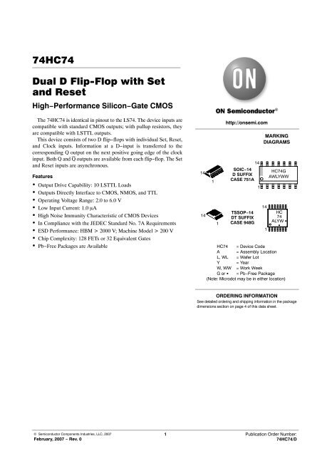
74HC74 Dual D FlipâFlop with Set and Reset
74HC74 Dual D FlipâFlop with Set and Reset
74HC74 Dual D FlipâFlop with Set and Reset

You also want an ePaper? Increase the reach of your titles
YUMPU automatically turns print PDFs into web optimized ePapers that Google loves.
<strong>74HC74</strong><br />
<strong>Dual</strong> D Flip−Flop <strong>with</strong> <strong>Set</strong><br />
<strong>and</strong> <strong>Reset</strong><br />
High−Performance Silicon−Gate CMOS<br />
The <strong>74HC74</strong> is identical in pinout to the LS74. The device inputs are<br />
compatible <strong>with</strong> st<strong>and</strong>ard CMOS outputs; <strong>with</strong> pullup resistors, they<br />
are compatible <strong>with</strong> LSTTL outputs.<br />
This device consists of two D flip−flops <strong>with</strong> individual <strong>Set</strong>, <strong>Reset</strong>,<br />
<strong>and</strong> Clock inputs. Information at a D−input is transferred to the<br />
corresponding Q output on the next positive going edge of the clock<br />
input. Both Q <strong>and</strong> Q outputs are available from each flip−flop. The <strong>Set</strong><br />
<strong>and</strong> <strong>Reset</strong> inputs are asynchronous.<br />
Features<br />
• Output Drive Capability: 10 LSTTL Loads<br />
• Outputs Directly Interface to CMOS, NMOS, <strong>and</strong> TTL<br />
• Operating Voltage Range: 2.0 to 6.0 V<br />
• Low Input Current: 1.0 A<br />
• High Noise Immunity Characteristic of CMOS Devices<br />
• In Compliance <strong>with</strong> the JEDEC St<strong>and</strong>ard No. 7A Requirements<br />
• ESD Performance: HBM 2000 V; Machine Model 200 V<br />
• Chip Complexity: 128 FETs or 32 Equivalent Gates<br />
• Pb−Free Packages are Available<br />
14<br />
14<br />
1<br />
1<br />
http://onsemi.com<br />
14<br />
SOIC−14<br />
D SUFFIX<br />
CASE 751A<br />
1<br />
TSSOP−14<br />
DT SUFFIX<br />
CASE 948G<br />
MARKING<br />
DIAGRAMS<br />
14<br />
HC74G<br />
AWLYWW<br />
HC<br />
74<br />
ALYW <br />
<br />
HC74 = Device Code<br />
A = Assembly Location<br />
L, WL = Wafer Lot<br />
Y = Year<br />
W, WW = Work Week<br />
G or = Pb−Free Package<br />
(Note: Microdot may be in either location)<br />
1<br />
ORDERING INFORMATION<br />
See detailed ordering <strong>and</strong> shipping information in the package<br />
dimensions section on page 4 of this data sheet.<br />
© Semiconductor Components Industries, LLC, 2007<br />
February, 2007 − Rev. 0<br />
1 Publication Order Number:<br />
<strong>74HC74</strong>/D
<strong>74HC74</strong><br />
PIN ASSIGNMENT<br />
LOGIC DIAGRAM<br />
RESET 1<br />
1<br />
14<br />
V CC<br />
RESET 1<br />
1<br />
DATA 1<br />
CLOCK 1<br />
SET 1<br />
Q1<br />
Q1<br />
GND<br />
2<br />
3<br />
4<br />
5<br />
6<br />
7<br />
FUNCTION TABLE<br />
Inputs<br />
Outputs<br />
<strong>Set</strong> <strong>Reset</strong> Clock Data Q Q<br />
L H X X H L<br />
H L X X L H<br />
L L X X H* H*<br />
H H H H L<br />
H H L L H<br />
H H L X No Change<br />
H H H X No Change<br />
H H X No Change<br />
13<br />
12<br />
11<br />
10<br />
9<br />
8<br />
RESET 2<br />
DATA 2<br />
CLOCK 2<br />
SET 2<br />
Q2<br />
Q2<br />
DATA 1<br />
CLOCK 1<br />
SET 1<br />
RESET 2<br />
DATA 2<br />
CLOCK 2<br />
SET 2<br />
2<br />
3<br />
4<br />
13<br />
12<br />
11<br />
10<br />
5<br />
6<br />
9<br />
8<br />
PIN 14 = V CC<br />
PIN 7 = GND<br />
Q1<br />
Q1<br />
Q2<br />
Q2<br />
*Both outputs will remain high as long as <strong>Set</strong> <strong>and</strong> <strong>Reset</strong> are low, but the output<br />
states are unpredictable if <strong>Set</strong> <strong>and</strong> <strong>Reset</strong> go high simultaneously.<br />
MAXIMUM RATINGS<br />
Symbol Parameter Value Unit<br />
ÎÎÎÎÎÎÎÎÎÎÎÎÎÎÎÎÎÎÎÎÎÎÎ<br />
V CC DC Supply Voltage (Referenced to GND) – 0.5 to + 7.0 V<br />
V in DC Input Voltage (Referenced to GND) – 0.5 to V CC + 0.5 V<br />
V out DC Output Voltage (Referenced to GND) – 0.5 to V CC + 0.5 V<br />
I in DC Input Current, per Pin ±20 mA<br />
I out DC Output Current, per Pin ±25 mA<br />
I CC DC Supply Current, V CC <strong>and</strong> GND Pins ±50 mA<br />
P D Power Dissipation in Still Air, SOIC Package† 500 mW<br />
TSSOP Package† 450<br />
T stg Storage Temperature – 65 to + 150 C<br />
T L<br />
Lead Temperature, 1 mm from Case for 10 Seconds<br />
(SOIC or TSSOP Package) 260<br />
300<br />
Stresses exceeding Maximum Ratings may damage the device. Maximum Ratings are stress<br />
ratings only. Functional operation above the Recommended Operating Conditions is not implied.<br />
Extended exposure to stresses above the Recommended Operating Conditions may affect device<br />
reliability.<br />
†Derating — SOIC Package: – 7 mW/C from 65 to 125C<br />
TSSOP Package: − 6.1 mW/C from 65 to 125C<br />
For high frequency or heavy load considerations, see Chapter 2 of the ON Semiconductor High−Speed CMOS Data Book (DL129/D).<br />
RECOMMENDED OPERATING CONDITIONS<br />
Symbol Parameter Min Max Unit<br />
V CC DC Supply Voltage (Referenced to GND) 2.0 6.0 V<br />
V in , V out DC Input Voltage, Output Voltage (Referenced to GND) 0 V CC V<br />
T A Operating Temperature, All Package Types – 55 + 125 C<br />
t r , t f Input Rise <strong>and</strong> Fall Time V CC = 2.0 V 0 1000 ns<br />
(Figures 1, 2, 3)<br />
V CC = 3.0 V<br />
V CC = 4.5 V<br />
V CC = 6.0 V<br />
0<br />
0<br />
0<br />
600<br />
500<br />
400<br />
C<br />
This device contains protection<br />
circuitry to guard against damage<br />
due to high static voltages or electric<br />
fields. However, precautions must<br />
be taken to avoid applications of any<br />
voltage higher than maximum rated<br />
voltages to this high−impedance circuit.<br />
For proper operation, V in <strong>and</strong><br />
V out should be constrained to the<br />
range GND (V in or V out ) V CC .<br />
Unused inputs must always be<br />
tied to an appropriate logic voltage<br />
level (e.g., either GND or V CC ).<br />
Unused outputs must be left open.<br />
http://onsemi.com<br />
2
<strong>74HC74</strong><br />
DC ELECTRICAL CHARACTERISTICS (Voltages Referenced to GND)<br />
Guaranteed Limit<br />
Symbol Parameter Test Conditions<br />
V CC<br />
(V)<br />
– 55 to<br />
25C 85C 125C<br />
Unit<br />
V IH<br />
Minimum High−Level Input<br />
Voltage<br />
V out = 0.1 V or V CC – 0.1 V<br />
|I out | 20 A<br />
2.0<br />
3.0<br />
4.5<br />
6.0<br />
1.5<br />
2.1<br />
3.15<br />
4.2<br />
1.5<br />
2.1<br />
3.15<br />
4.2<br />
1.5<br />
2.1<br />
3.15<br />
4.2<br />
V<br />
V IL<br />
Maximum Low−Level Input<br />
Voltage<br />
V out = 0.1 V or V CC – 0.1 V<br />
|I out | 20 A<br />
2.0<br />
3.0<br />
4.5<br />
6.0<br />
0.5<br />
0.9<br />
1.35<br />
1.8<br />
0.5<br />
0.9<br />
1.35<br />
1.8<br />
0.5<br />
0.9<br />
1.35<br />
1.8<br />
V<br />
V OH<br />
V OL<br />
Minimum High−Level Output<br />
Voltage<br />
Maximum Low−Level Output<br />
Voltage<br />
V in = V IH or V IL<br />
|I out | 20 A<br />
V in = V IH or V IL<br />
V in = V IH or V IL<br />
|I out | 20 A<br />
V in = V IH or V IL<br />
|I out | 2.4 mA<br />
|I out | 4.0 mA<br />
|I out | 5.2 mA<br />
|I out | 2.4 mA<br />
|I out | 4.0 mA<br />
|I out | 5.2 mA<br />
2.0<br />
4.5<br />
6.0<br />
3.0<br />
4.5<br />
6.0<br />
2.0<br />
4.5<br />
6.0<br />
3.0<br />
4.5<br />
6.0<br />
1.9<br />
4.4<br />
5.9<br />
2.48<br />
3.98<br />
5.48<br />
0.1<br />
0.1<br />
0.1<br />
0.26<br />
0.26<br />
0.26<br />
1.9<br />
4.4<br />
5.9<br />
2.34<br />
3.84<br />
5.34<br />
0.1<br />
0.1<br />
0.1<br />
0.33<br />
0.33<br />
0.33<br />
I in Maximum Input Leakage Current V in = V CC or GND 6.0 ±0.1 ±1.0 ±1.0 A<br />
I CC<br />
Maximum Quiescent Supply<br />
Current (per Package)<br />
V in = V CC or GND<br />
I out = 0 A<br />
1.9<br />
4.4<br />
5.9<br />
2.2<br />
3.7<br />
5.2<br />
0.1<br />
0.1<br />
0.1<br />
0.4<br />
0.4<br />
0.4<br />
6.0 2.0 20 80 A<br />
NOTE: Information on typical parametric values can be found in Chapter 2 of the ON Semiconductor High−Speed CMOS Data Book<br />
(DL129/D).<br />
AC ELECTRICAL CHARACTERISTICS (C L = 50 pF, Input t r = t f = 6.0 ns)<br />
Symbol<br />
f max<br />
t PLH ,<br />
t PHL<br />
t PLH ,<br />
t PHL<br />
t TLH ,<br />
t THL<br />
Parameter<br />
Maximum Clock Frequency (50% Duty Cycle)<br />
(Figures 1 <strong>and</strong> 4)<br />
Maximum Propagation Delay, Clock to Q or Q<br />
(Figures 1 <strong>and</strong> 4)<br />
Maximum Propagation Delay, <strong>Set</strong> or <strong>Reset</strong> to Q or Q<br />
(Figures 2 <strong>and</strong> 4)<br />
Maximum Output Transition Time, Any Output<br />
(Figures 1 <strong>and</strong> 4)<br />
V CC<br />
(V)<br />
2.0<br />
3.0<br />
4.5<br />
6.0<br />
2.0<br />
3.0<br />
4.5<br />
6.0<br />
2.0<br />
3.0<br />
4.5<br />
6.0<br />
2.0<br />
3.0<br />
4.5<br />
6.0<br />
Guaranteed Limit<br />
– 55 to<br />
25C 85C 125C<br />
C in Maximum Input Capacitance — 10 10 10 pF<br />
NOTE: For propagation delays <strong>with</strong> loads other than 50 pF, <strong>and</strong> information on typical parametric values, see Chapter 2 of the ON<br />
Semiconductor High−Speed CMOS Data Book (DL129/D).<br />
6.0<br />
15<br />
30<br />
35<br />
100<br />
75<br />
20<br />
17<br />
105<br />
80<br />
21<br />
18<br />
75<br />
30<br />
15<br />
13<br />
4.8<br />
10<br />
24<br />
28<br />
125<br />
90<br />
25<br />
21<br />
130<br />
95<br />
26<br />
22<br />
95<br />
40<br />
19<br />
16<br />
4.0<br />
8.0<br />
20<br />
24<br />
150<br />
120<br />
30<br />
26<br />
160<br />
130<br />
32<br />
27<br />
110<br />
55<br />
22<br />
19<br />
Typical @ 25°C, V CC = 5.0 V<br />
C PD Power Dissipation Capacitance (Per Flip−Flop)*<br />
32<br />
pF<br />
* Used to determine the no−load dynamic power consumption: P D = C PD V 2 CC f + I CC V CC . For load considerations, see Chapter 2 of the<br />
ON Semiconductor High−Speed CMOS Data Book (DL129/D).<br />
V<br />
V<br />
Unit<br />
MHz<br />
ns<br />
ns<br />
ns<br />
http://onsemi.com<br />
3
<strong>74HC74</strong><br />
TIMING REQUIREMENTS (Input t r = t f = 6.0 ns)<br />
Guaranteed Limit<br />
Symbol<br />
Parameter<br />
V CC<br />
(V)<br />
– 55 to<br />
25C 85C 125C<br />
Unit<br />
t su<br />
Minimum <strong>Set</strong>up Time, Data to Clock<br />
(Figure 3)<br />
2.0<br />
3.0<br />
4.5<br />
6.0<br />
80<br />
35<br />
16<br />
14<br />
100<br />
45<br />
20<br />
17<br />
120<br />
55<br />
24<br />
20<br />
ns<br />
t h<br />
Minimum Hold Time, Clock to Data<br />
(Figure 3)<br />
2.0<br />
3.0<br />
4.5<br />
6.0<br />
3.0<br />
3.0<br />
3.0<br />
3.0<br />
3.0<br />
3.0<br />
3.0<br />
3.0<br />
3.0<br />
3.0<br />
3.0<br />
3.0<br />
ns<br />
t rec<br />
Minimum Recovery Time, <strong>Set</strong> or <strong>Reset</strong> Inactive to Clock<br />
(Figure 2)<br />
2.0<br />
3.0<br />
4.5<br />
6.0<br />
8.0<br />
8.0<br />
8.0<br />
8.0<br />
8.0<br />
8.0<br />
8.0<br />
8.0<br />
8.0<br />
8.0<br />
8.0<br />
8.0<br />
ns<br />
t w<br />
Minimum Pulse Width, Clock<br />
(Figure 1)<br />
2.0<br />
3.0<br />
4.5<br />
6.0<br />
60<br />
25<br />
12<br />
10<br />
75<br />
30<br />
15<br />
13<br />
90<br />
40<br />
18<br />
15<br />
ns<br />
t w<br />
Minimum Pulse Width, <strong>Set</strong> or <strong>Reset</strong><br />
(Figure 2)<br />
2.0<br />
3.0<br />
4.5<br />
6.0<br />
60<br />
25<br />
12<br />
10<br />
75<br />
30<br />
15<br />
13<br />
90<br />
40<br />
18<br />
15<br />
ns<br />
t r , t f<br />
Maximum Input Rise <strong>and</strong> Fall Times<br />
(Figures 1, 2, 3)<br />
2.0<br />
3.0<br />
4.5<br />
6.0<br />
1000<br />
800<br />
500<br />
400<br />
1000<br />
800<br />
500<br />
400<br />
1000<br />
800<br />
500<br />
400<br />
ns<br />
ORDERING INFORMATION<br />
Device Package Shipping †<br />
<strong>74HC74</strong>D<br />
<strong>74HC74</strong>DG<br />
<strong>74HC74</strong>DR2<br />
<strong>74HC74</strong>DR2G<br />
<strong>74HC74</strong>DTR2<br />
<strong>74HC74</strong>DTR2G<br />
SOIC−14<br />
SOIC−14<br />
(Pb−Free)<br />
SOIC−14<br />
SOIC−14<br />
(Pb−Free)<br />
TSSOP−14*<br />
TSSOP−14*<br />
55 Units / Rail<br />
2500 / Tape & Reel<br />
†For information on tape <strong>and</strong> reel specifications, including part orientation <strong>and</strong> tape sizes, please refer to our Tape <strong>and</strong> Reel Packaging<br />
Specifications Brochure, BRD8011/D.<br />
*This package is inherently Pb−Free.<br />
http://onsemi.com<br />
4
<strong>74HC74</strong><br />
SWITCHING WAVEFORMS<br />
t w<br />
CLOCK<br />
90%<br />
50%<br />
10%<br />
t w<br />
t f t r<br />
V CC<br />
1/f max<br />
GND<br />
SET OR<br />
RESET<br />
Q OR Q<br />
50%<br />
t PHL<br />
50%<br />
V CC<br />
GND<br />
DATA<br />
CLOCK<br />
Q or Q<br />
t PLH<br />
t PHL<br />
t rec<br />
90%<br />
50%<br />
10%<br />
Q OR Q<br />
50%<br />
t su t h UNDER<br />
V CC<br />
TEST<br />
C L *<br />
t TLH t THL<br />
CLOCK<br />
50%<br />
Figure 1.<br />
Figure 2.<br />
VALID<br />
TEST POINT<br />
V CC<br />
50%<br />
OUTPUT<br />
GND<br />
DEVICE<br />
50%<br />
GND<br />
t PLH<br />
*Includes all probe <strong>and</strong> jig capacitance<br />
V CC<br />
GND<br />
Figure 3.<br />
Figure 4.<br />
4, 10<br />
SET<br />
2, 12<br />
DATA<br />
CLOCK 3, 11 5, 9<br />
Q<br />
6, 8<br />
Q<br />
1, 13<br />
RESET<br />
Figure 5. EXPANDED LOGIC DIAGRAM<br />
http://onsemi.com<br />
5
<strong>74HC74</strong><br />
PACKAGE DIMENSIONS<br />
SOIC−14<br />
CASE 751A−03<br />
ISSUE H<br />
−T−<br />
SEATING<br />
PLANE<br />
G<br />
−A−<br />
14 8<br />
1<br />
D 14 PL<br />
7<br />
−B−<br />
K<br />
P 7 PL<br />
C<br />
0.25 (0.010) M T B S A S<br />
0.25 (0.010) M B M<br />
NOTES:<br />
1. DIMENSIONING AND TOLERANCING PER<br />
ANSI Y14.5M, 1982.<br />
2. CONTROLLING DIMENSION: MILLIMETER.<br />
3. DIMENSIONS A AND B DO NOT INCLUDE<br />
MOLD PROTRUSION.<br />
4. MAXIMUM MOLD PROTRUSION 0.15 (0.006)<br />
PER SIDE.<br />
5. DIMENSION D DOES NOT INCLUDE<br />
DAMBAR PROTRUSION. ALLOWABLE<br />
DAMBAR PROTRUSION SHALL BE 0.127<br />
(0.005) TOTAL IN EXCESS OF THE D<br />
DIMENSION AT MAXIMUM MATERIAL<br />
CONDITION.<br />
MILLIMETERS INCHES<br />
R X 45 F<br />
DIM MIN MAX MIN MAX<br />
A 8.55 8.75 0.337 0.344<br />
B 3.80 4.00 0.150 0.157<br />
C 1.35 1.75 0.054 0.068<br />
D 0.35 0.49 0.014 0.019<br />
M<br />
J<br />
F 0.40 1.25 0.016 0.049<br />
G 1.27 BSC 0.050 BSC<br />
J 0.19 0.25 0.008 0.009<br />
K 0.10 0.25 0.004 0.009<br />
M 0 7 0 7 <br />
P 5.80 6.20 0.228 0.244<br />
R 0.25 0.50 0.010 0.019<br />
SOLDERING FOOTPRINT*<br />
14X<br />
0.58<br />
1<br />
7X<br />
7.04<br />
14X<br />
1.52<br />
1.27<br />
PITCH<br />
DIMENSIONS: MILLIMETERS<br />
*For additional information on our Pb−Free strategy <strong>and</strong> soldering<br />
details, please download the ON Semiconductor Soldering <strong>and</strong><br />
Mounting Techniques Reference Manual, SOLDERRM/D.<br />
http://onsemi.com<br />
6
<strong>74HC74</strong><br />
PACKAGE DIMENSIONS<br />
TSSOP−14<br />
CASE 948G−01<br />
ISSUE B<br />
0.15 (0.006) T<br />
0.15 (0.006) T<br />
L<br />
0.10 (0.004)<br />
−T− SEATING<br />
PLANE<br />
U<br />
U<br />
S<br />
2X L/2<br />
PIN 1<br />
IDENT.<br />
S<br />
D<br />
C<br />
14<br />
1<br />
14X K REF<br />
0.10 (0.004) M T U S V S<br />
N<br />
8<br />
0.25 (0.010)<br />
M<br />
B<br />
−U−<br />
7<br />
A<br />
−V−<br />
G<br />
H<br />
N<br />
J J1<br />
F<br />
DETAIL E<br />
K<br />
K1<br />
DETAIL E<br />
ÇÇÇ<br />
ÉÉÉ ÇÇÇ<br />
SECTION N−N<br />
ÉÉÉ ÇÇÇ<br />
−W−<br />
NOTES:<br />
1. DIMENSIONING AND TOLERANCING PER<br />
ANSI Y14.5M, 1982.<br />
2. CONTROLLING DIMENSION: MILLIMETER.<br />
3. DIMENSION A DOES NOT INCLUDE MOLD<br />
FLASH, PROTRUSIONS OR GATE BURRS.<br />
MOLD FLASH OR GATE BURRS SHALL NOT<br />
EXCEED 0.15 (0.006) PER SIDE.<br />
4. DIMENSION B DOES NOT INCLUDE<br />
INTERLEAD FLASH OR PROTRUSION.<br />
INTERLEAD FLASH OR PROTRUSION SHALL<br />
NOT EXCEED 0.25 (0.010) PER SIDE.<br />
5. DIMENSION K DOES NOT INCLUDE<br />
DAMBAR PROTRUSION. ALLOWABLE<br />
DAMBAR PROTRUSION SHALL BE 0.08<br />
(0.003) TOTAL IN EXCESS OF THE K<br />
DIMENSION AT MAXIMUM MATERIAL<br />
CONDITION.<br />
6. TERMINAL NUMBERS ARE SHOWN FOR<br />
REFERENCE ONLY.<br />
7. DIMENSION A AND B ARE TO BE<br />
DETERMINED AT DATUM PLANE −W−.<br />
MILLIMETERS INCHES<br />
DIM MIN MAX MIN MAX<br />
A 4.90 5.10 0.193 0.200<br />
B 4.30 4.50 0.169 0.177<br />
C −−− 1.20 −−− 0.047<br />
D 0.05 0.15 0.002 0.006<br />
F 0.50 0.75 0.020 0.030<br />
G 0.65 BSC 0.026 BSC<br />
H 0.50 0.60 0.020 0.024<br />
J 0.09 0.20 0.004 0.008<br />
J1 0.09 0.16 0.004 0.006<br />
K 0.19 0.30 0.007 0.012<br />
K1 0.19 0.25 0.007 0.010<br />
L 6.40 BSC 0.252 BSC<br />
M 0 8 0 8 <br />
SOLDERING FOOTPRINT*<br />
7.06<br />
1<br />
0.65<br />
PITCH<br />
14X<br />
0.36<br />
14X<br />
1.26<br />
DIMENSIONS: MILLIMETERS<br />
*For additional information on our Pb−Free strategy <strong>and</strong> soldering<br />
details, please download the ON Semiconductor Soldering <strong>and</strong><br />
Mounting Techniques Reference Manual, SOLDERRM/D.<br />
http://onsemi.com<br />
7
<strong>74HC74</strong><br />
ON Semiconductor <strong>and</strong> are registered trademarks of Semiconductor Components Industries, LLC (SCILLC). SCILLC reserves the right to make changes <strong>with</strong>out further notice<br />
to any products herein. SCILLC makes no warranty, representation or guarantee regarding the suitability of its products for any particular purpose, nor does SCILLC assume any liability<br />
arising out of the application or use of any product or circuit, <strong>and</strong> specifically disclaims any <strong>and</strong> all liability, including <strong>with</strong>out limitation special, consequential or incidental damages.<br />
“Typical” parameters which may be provided in SCILLC data sheets <strong>and</strong>/or specifications can <strong>and</strong> do vary in different applications <strong>and</strong> actual performance may vary over time. All<br />
operating parameters, including “Typicals” must be validated for each customer application by customer’s technical experts. SCILLC does not convey any license under its patent rights<br />
nor the rights of others. SCILLC products are not designed, intended, or authorized for use as components in systems intended for surgical implant into the body, or other applications<br />
intended to support or sustain life, or for any other application in which the failure of the SCILLC product could create a situation where personal injury or death may occur. Should<br />
Buyer purchase or use SCILLC products for any such unintended or unauthorized application, Buyer shall indemnify <strong>and</strong> hold SCILLC <strong>and</strong> its officers, employees, subsidiaries, affiliates,<br />
<strong>and</strong> distributors harmless against all claims, costs, damages, <strong>and</strong> expenses, <strong>and</strong> reasonable attorney fees arising out of, directly or indirectly, any claim of personal injury or death<br />
associated <strong>with</strong> such unintended or unauthorized use, even if such claim alleges that SCILLC was negligent regarding the design or manufacture of the part. SCILLC is an Equal<br />
Opportunity/Affirmative Action Employer. This literature is subject to all applicable copyright laws <strong>and</strong> is not for resale in any manner.<br />
PUBLICATION ORDERING INFORMATION<br />
LITERATURE FULFILLMENT:<br />
Literature Distribution Center for ON Semiconductor<br />
P.O. Box 5163, Denver, Colorado 80217 USA<br />
Phone: 303−675−2175 or 800−344−3860 Toll Free USA/Canada<br />
Fax: 303−675−2176 or 800−344−3867 Toll Free USA/Canada<br />
Email: orderlit@onsemi.com<br />
N. American Technical Support: 800−282−9855 Toll Free<br />
USA/Canada<br />
Europe, Middle East <strong>and</strong> Africa Technical Support:<br />
Phone: 421 33 790 2910<br />
Japan Customer Focus Center<br />
Phone: 81−3−5773−3850<br />
http://onsemi.com<br />
8<br />
ON Semiconductor Website: www.onsemi.com<br />
Order Literature: http://www.onsemi.com/orderlit<br />
For additional information, please contact your local<br />
Sales Representative<br />
<strong>74HC74</strong>/D