DM74LS157/DM74LS158 Quad 2-Line to 1-Line Data Selectors ...
DM74LS157/DM74LS158 Quad 2-Line to 1-Line Data Selectors ...
DM74LS157/DM74LS158 Quad 2-Line to 1-Line Data Selectors ...

Create successful ePaper yourself
Turn your PDF publications into a flip-book with our unique Google optimized e-Paper software.
<strong>DM74LS157</strong>/<strong>DM74LS158</strong><br />
<strong>Quad</strong> 2-<strong>Line</strong> <strong>to</strong> 1-<strong>Line</strong> <strong>Data</strong> Selec<strong>to</strong>rs/Multiplexers<br />
General Description<br />
These data selec<strong>to</strong>rs/multiplexers contain inverters and drivers<br />
<strong>to</strong> supply full on-chip data selection <strong>to</strong> the four output<br />
gates. A separate strobe input is provided. A 4-bit word is selected<br />
from one of two sources and is routed <strong>to</strong> the four outputs.<br />
The LS157 presents true data whereas the LS158 presents<br />
inverted data <strong>to</strong> minimize propagation delay time.<br />
Applications<br />
n Expand any data input point<br />
n Multiplex dual data buses<br />
n Generate four functions of two variables (one variable is<br />
common)<br />
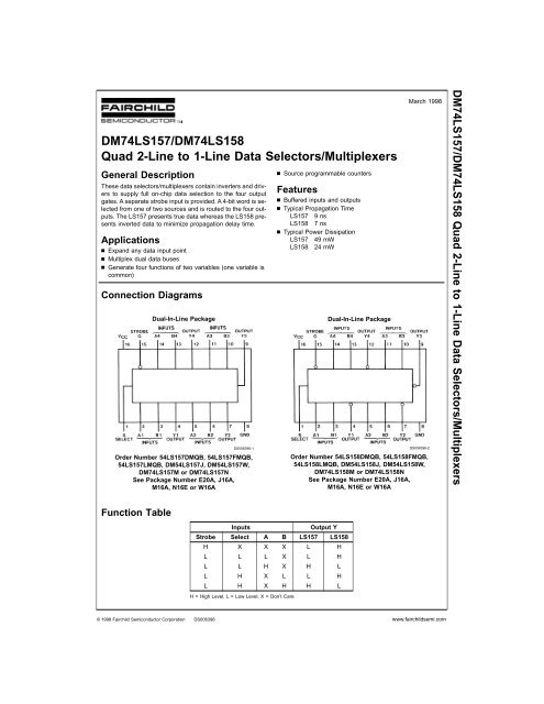
Connection Diagrams<br />
Dual-In-<strong>Line</strong> Package<br />
DS006396-1<br />
Order Number 54LS157DMQB, 54LS157FMQB,<br />
54LS157LMQB, DM54LS157J, DM54LS157W,<br />
<strong>DM74LS157</strong>M or <strong>DM74LS157</strong>N<br />
See Package Number E20A, J16A,<br />
M16A, N16E or W16A<br />
n Source programmable counters<br />
Features<br />
n Buffered inputs and outputs<br />
n Typical Propagation Time<br />
LS157 9 ns<br />
LS158 7 ns<br />
n Typical Power Dissipation<br />
LS157 49 mW<br />
LS158 24 mW<br />
Dual-In-<strong>Line</strong> Package<br />
March 1998<br />
DS006396-2<br />
Order Number 54LS158DMQB, 54LS158FMQB,<br />
54LS158LMQB, DM54LS158J, DM54LS158W,<br />
<strong>DM74LS158</strong>M or <strong>DM74LS158</strong>N<br />
See Package Number E20A, J16A,<br />
M16A, N16E or W16A<br />
<strong>DM74LS157</strong>/<strong>DM74LS158</strong> <strong>Quad</strong> 2-<strong>Line</strong> <strong>to</strong> 1-<strong>Line</strong> <strong>Data</strong> Selec<strong>to</strong>rs/Multiplexers<br />
Function Table<br />
Inputs<br />
Output Y<br />
Strobe Select A B LS157 LS158<br />
H X X X L H<br />
L L L X L H<br />
L L H X H L<br />
L H X L L H<br />
L H X H H L<br />
H = High Level, L = Low Level, X = Don’t Care<br />
© 1998 Fairchild Semiconduc<strong>to</strong>r Corporation DS006396 www.fairchildsemi.com
Absolute Maximum Ratings (Note 1)<br />
DM54LS and 54LS<br />
−55˚C <strong>to</strong> +125˚C<br />
Supply Voltage<br />
Input Voltage<br />
7V<br />
7V<br />
DM74LS<br />
S<strong>to</strong>rage Temperature Range<br />
0˚C <strong>to</strong> +70˚C<br />
−65˚C <strong>to</strong> +150˚C<br />
Operating Free Air Temperature Range<br />
Recommended Operating Conditions<br />
Symbol Parameter DM54LS157 <strong>DM74LS157</strong> Units<br />
Min Nom Max Min Nom Max<br />
V CC Supply Voltage 4.5 5 5.5 4.75 5 5.25 V<br />
V IH High Level Input Voltage 2 2 V<br />
V IL Low Level Input Voltage 0.7 0.8 V<br />
I OH High Level Output Current −0.4 −0.4 mA<br />
I OL Low Level Output Current 4 8 mA<br />
T A Free Air Operating Temperature −55 125 0 70 ˚C<br />
Note 1: The “Absolute Maximum Ratings” are those values beyond which the safety of the device cannot be guaranteed. The device should not be operated at these<br />
limits. The parametric values defined in the “Electrical Characteristics” table are not guaranteed at the absolute maximum ratings. The “Recommended Operating<br />
Conditions” table will define the conditions for actual device operation.<br />
’LS157 Electrical Characteristics<br />
over recommended operating free air temperature range (unless otherwise noted)<br />
Symbol Parameter Conditions Min Typ Max Units<br />
(Note 2)<br />
V I Input Clamp Voltage V CC<br />
= Min, I I<br />
= −18 mA −1.5 V<br />
V OH High Level Output V CC<br />
= Min, I OH<br />
= Max DM54 2.5 3.4 V<br />
Voltage V IL<br />
= Max, V IH<br />
= Min DM74 2.7 3.4<br />
V OL Low Level Output V CC<br />
= Min, I OL<br />
= Max DM54 0.25 0.4<br />
Voltage V IL<br />
= Max, V IH<br />
= Min DM74 0.35 0.5 V<br />
I OL<br />
= 4 mA, V CC<br />
= Min DM74 0.25 0.4<br />
I I Input Current @ Max V CC<br />
= Max S or G 0.2 mA<br />
Input Voltage V I<br />
= 7V A or B 0.1<br />
I IH High Level Input V CC<br />
= Max S or G 40 µA<br />
Current V I<br />
= 2.7V A or B 20<br />
I IL Low Level Input V CC<br />
= Max S or G −0.8 mA<br />
Current V I<br />
= 0.4V A or B −0.4<br />
I OS Short Circuit V CC<br />
= Max DM54 −20 −100 mA<br />
Output Current (Note 3) DM74 −20 −100<br />
I CC Supply Current V CC<br />
= Max (Note 4) 9.7 16 mA<br />
Note 2: All typicals are at V CC = 5V, T A = 25˚C.<br />
Note 3: Not more than one output should be shorted at a time, and the duration should not exceed one second.<br />
Note 4: I CC is measured with 4.5V applied <strong>to</strong> all inputs and all outputs open.<br />
’LS157 Switching Characteristics<br />
at V CC<br />
= 5V and T A<br />
= 25˚C<br />
From (Input)<br />
R L<br />
= 2kΩ<br />
Symbol Parameter To (Output) C L<br />
= 15 pF C L<br />
= 50 pF Units<br />
Min Max Min Max<br />
t PLH Propagation Delay Time <strong>Data</strong> 14 18 ns<br />
Low <strong>to</strong> High Level Output<br />
<strong>to</strong> Y<br />
t PHL Propagation Delay Time <strong>Data</strong> 14 23 ns<br />
High <strong>to</strong> Low Level Output<br />
<strong>to</strong> Y<br />
www.fairchildsemi.com 2
’LS157 Switching Characteristics (Continued)<br />
at V CC<br />
= 5V and T A<br />
= 25˚C<br />
From (Input)<br />
R L<br />
= 2kΩ<br />
Symbol Parameter To (Output) C L<br />
= 15 pF C L<br />
= 50 pF Units<br />
Min Max Min Max<br />
t PLH Propagation Delay Time Strobe 20 24 ns<br />
Low <strong>to</strong> High Level Output<br />
<strong>to</strong> Y<br />
t PHL Propagation Delay Time Strobe 21 30 ns<br />
High <strong>to</strong> Low Level Output<br />
<strong>to</strong> Y<br />
t PLH Propagation Delay Time Select 23 28 ns<br />
Low <strong>to</strong> High Level Output<br />
<strong>to</strong> Y<br />
t PHL Propagation Delay Time Select 27 32 ns<br />
High <strong>to</strong> Low Level Output<br />
<strong>to</strong> Y<br />
Recommended Operating Conditions<br />
Symbol Parameter DM54LS158 <strong>DM74LS158</strong> Units<br />
Min Nom Max Min Nom Max<br />
V CC Supply Voltage 4.5 5 5.5 4.75 5 5.25 V<br />
V IH High Level Input Voltage 2 2 V<br />
V IL Low Level Input Voltage 0.7 0.8 V<br />
I OH High Level Output Current −0.4 −0.4 mA<br />
I OL Low Level Output Current 4 8 mA<br />
T A Free Air Operating Temperature −55 125 0 70 ˚C<br />
’LS158 Electrical Characteristics<br />
over recommended operating free air temperature range (unless otherwise noted)<br />
Symbol Parameter Conditions Min Typ Max Units<br />
(Note 5)<br />
V I Input Clamp Voltage V CC<br />
= Min, I I<br />
= −18 mA −1.5 V<br />
V OH High Level Output V CC<br />
= Min, I OH<br />
= Max DM54 2.5 3.4 V<br />
Voltage V IL<br />
= Max, V IH<br />
= Min DM74 2.7 3.4<br />
V OL Low Level Output V CC<br />
= Min, I OL<br />
= Max DM54 0.25 0.4<br />
Voltage V IL<br />
= Max, V IH<br />
= Min DM74 0.35 0.5 V<br />
I OL<br />
= 4 mA, V CC<br />
= Min DM74 0.25 0.4<br />
I I Input Current @ Max V CC<br />
= Max S or G 0.2 mA<br />
Input Voltage V I<br />
= 7V A or B 0.1<br />
I IH High Level Input V CC<br />
= Max S or G 40 µA<br />
Current V I<br />
= 2.7V A or B 20<br />
I IL Low Level Input V CC<br />
= Max S or G −0.8 mA<br />
Current V I<br />
= 0.4V A or B −0.4<br />
I OS Short Circuit V CC<br />
= Max DM54 −20 −100 mA<br />
Output Current (Note 6) DM74 −20 −100<br />
I CC Supply Current V CC<br />
= Max (Note 7) 4.8 8 mA<br />
Note 5: All typicals are at V CC = 5V, T A = 25˚C.<br />
Note 6: Not more than one output should be shorted at a time, and the duration should not exceed one second.<br />
Note 7: I CC is measured with 4.5V applied <strong>to</strong> all inputs and all outputs open.<br />
3 www.fairchildsemi.com
’LS158 Switching Characteristics<br />
at V CC<br />
= 5V and T A<br />
= 25˚C<br />
From (Input)<br />
R L<br />
= 2kΩ<br />
Symbol Parameter To (Output) C L<br />
= 15 pF C L<br />
= 50 pF Units<br />
Min Max Min Max<br />
t PLH Propagation Delay Time <strong>Data</strong> 12 18 ns<br />
Low <strong>to</strong> High Level Output<br />
<strong>to</strong> Y<br />
t PHL Propagation Delay Time <strong>Data</strong> 12 21 ns<br />
High <strong>to</strong> Low Level Output<br />
<strong>to</strong> Y<br />
t PLH Propagation Delay Time Strobe 17 23 ns<br />
Low <strong>to</strong> High Level Output<br />
<strong>to</strong> Y<br />
t PHL Propagation Delay Time Strobe 18 28 ns<br />
High <strong>to</strong> Low Level Output<br />
<strong>to</strong> Y<br />
t PLH Propagation Delay Time Select 20 24 ns<br />
Low <strong>to</strong> High Level Output<br />
<strong>to</strong> Y<br />
t PHL Propagation Delay Time Select 24 36 ns<br />
High <strong>to</strong> Low Level Output<br />
<strong>to</strong> Y<br />
Logic Diagrams<br />
LS157<br />
LS158<br />
DS006396-3<br />
DS006396-4<br />
www.fairchildsemi.com 4
Physical Dimensions inches (millimeters) unless otherwise noted<br />
Ceramic Leadless Chip Carrier Package (E)<br />
Order Number 54LS157LMQB or 54LS158LMQB<br />
Package Number E20A<br />
16-Lead Ceramic Dual-In-<strong>Line</strong> Package (J)<br />
Order Number 54LS157DMQB, 54LS158DMQB, DM54LS157J or DM54LS158J<br />
Package Number J16A<br />
www.fairchildsemi.com 6
Physical Dimensions inches (millimeters) unless otherwise noted (Continued)<br />
16-Lead Small Outline Molded Package (M)<br />
Order Number <strong>DM74LS157</strong>M or <strong>DM74LS158</strong>M<br />
Package Number M16A<br />
16-Lead Molded Dual-In-<strong>Line</strong> Package (N)<br />
Order Number <strong>DM74LS157</strong>N or <strong>DM74LS158</strong>N<br />
Package Number N16E<br />
7 www.fairchildsemi.com
<strong>DM74LS157</strong>/<strong>DM74LS158</strong> <strong>Quad</strong> 2-<strong>Line</strong> <strong>to</strong> 1-<strong>Line</strong> <strong>Data</strong> Selec<strong>to</strong>rs/Multiplexers<br />
Physical Dimensions inches (millimeters) unless otherwise noted (Continued)<br />
LIFE SUPPORT POLICY<br />
16-Lead Ceramic Flat Package (W)<br />
Order Number 54LS157FMQB, 54LS158FMQB, DM54LS157W or DM54LS158W<br />
Package Number W16A<br />
FAIRCHILD’S PRODUCTS ARE NOT AUTHORIZED FOR USE AS CRITICAL COMPONENTS IN LIFE SUPPORT DE-<br />
VICES OR SYSTEMS WITHOUT THE EXPRESS WRITTEN APPROVAL OF THE PRESIDENT OF FAIRCHILD SEMI-<br />
CONDUCTOR CORPORATION. As used herein:<br />
1. Life support devices or systems are devices or systems<br />
which, (a) are intended for surgical implant in<strong>to</strong><br />
the body, or (b) support or sustain life, and (c) whose<br />
failure <strong>to</strong> perform when properly used in accordance<br />
with instructions for use provided in the labeling, can<br />
be reasonably expected <strong>to</strong> result in a significant injury<br />
<strong>to</strong> the user.<br />
2. A critical component in any component of a life support<br />
device or system whose failure <strong>to</strong> perform can be reasonably<br />
expected <strong>to</strong> cause the failure of the life support<br />
device or system, or <strong>to</strong> affect its safety or effectiveness.<br />
Fairchild Semiconduc<strong>to</strong>r<br />
Corporation<br />
Americas<br />
Cus<strong>to</strong>mer Response Center<br />
Tel: 1-888-522-5372<br />
www.fairchildsemi.com<br />
Fairchild Semiconduc<strong>to</strong>r<br />
Europe<br />
Fax: +49 (0) 1 80-530 85 86<br />
Email: europe.support@nsc.com<br />
Deutsch Tel: +49 (0) 8 141-35-0<br />
English Tel: +44 (0) 1 793-85-68-56<br />
Italy Tel: +39 (0) 2 57 5631<br />
Fairchild Semiconduc<strong>to</strong>r<br />
Hong Kong Ltd.<br />
13th Floor, Straight Block,<br />
Ocean Centre, 5 Can<strong>to</strong>n Rd.<br />
Tsimshatsui, Kowloon<br />
Hong Kong<br />
Tel: +852 2737-7200<br />
Fax: +852 2314-0061<br />
National Semiconduc<strong>to</strong>r<br />
Japan Ltd.<br />
Tel: 81-3-5620-6175<br />
Fax: 81-3-5620-6179<br />
Fairchild does not assume any responsibility for use of any circuitry described, no circuit patent licenses are implied and Fairchild reserves the right at any time without notice <strong>to</strong> change said circuitry and specifications.