tda7294 100V - 100W DMOS audio amplifier - 320Volt
tda7294 100V - 100W DMOS audio amplifier - 320Volt
tda7294 100V - 100W DMOS audio amplifier - 320Volt

You also want an ePaper? Increase the reach of your titles
YUMPU automatically turns print PDFs into web optimized ePapers that Google loves.
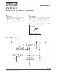
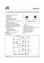
TDA7294<br />
APPLICATION INFORMATION<br />
HIGH-EFFICIENCY<br />
Constraints of implementing high power solutions<br />
are the power dissipation and the size of the<br />
power supply. These are both due to the low efficiency<br />
of conventional AB class <strong>amplifier</strong> approaches.<br />
Here below (figure 18) is described a circuit proposal<br />
for a high efficiency <strong>amplifier</strong> which can be<br />
adopted for both HI-FI and CAR-RADIO applications.<br />
The TDA7294 is a monolithic MOS power <strong>amplifier</strong><br />
which can be operated at 80V supply voltage<br />
(<strong>100V</strong> with no signal applied) while delivering output<br />
currents up to ±10 A.<br />
This allows the use of this device as a very high<br />
power <strong>amplifier</strong> (up to 180W as peak power with<br />
T.H.D.=10 % and Rl = 4 Ohm); the only drawback<br />
is the power dissipation, hardly manageable in<br />
the above power range.<br />
Figure 20 shows the power dissipation versus<br />
output power curve for a class AB <strong>amplifier</strong>, compared<br />
with a high efficiency one.<br />
In order to dimension the heatsink (and the power<br />
supply), a generally used average output power<br />
value is one tenth of the maximum output power<br />
at T.H.D.=10 %.<br />
From fig. 20, where the maximum power is<br />
around 200 W, we get an average of 20 W, in this<br />
condition, for a class AB <strong>amplifier</strong> the average<br />
power dissipation is equal to 65 W.<br />
The typical junction-to-case thermal resistance of<br />
the TDA7294 is 1 o C/W (max= 1.5 o C/W). To<br />
avoid that, in worst case conditions, the chip temperature<br />
exceedes 150 o C, the thermal resistance<br />
of the heatsink must be 0.038 o C/W (@ max ambient<br />
temperature of 50 o C).<br />
As the above value is pratically unreachable; a<br />
high efficiency system is needed in those cases<br />
where the continuous RMS output power is higher<br />
than 50-60 W.<br />
The TDA7294 was designed to work also in<br />
higher efficiency way.<br />
For this reason there are four power supply pins:<br />
two intended for the signal part and two for the<br />
power part.<br />
T1 and T2 are two power transistors that only operate<br />
when the output power reaches a certain<br />
threshold (e.g. 20 W). If the output power increases,<br />
these transistors are switched on during<br />
the portion of the signal where more output voltage<br />
swing is needed, thus "bootstrapping" the<br />
power supply pins (#13 and #15).<br />
The current generators formed by T4, T7, zener<br />
Figure 18: High Efficiency Application Circuit<br />
+40V<br />
+20V<br />
D1 BYW98100<br />
T1<br />
BDX53A<br />
270<br />
T3<br />
BC394<br />
R4<br />
270<br />
T4<br />
BC393<br />
R5<br />
270<br />
T5<br />
BC393<br />
GND<br />
C1<br />
1000µF<br />
C2<br />
1000µF<br />
C3<br />
100nF<br />
C4<br />
100nF<br />
C5<br />
1000µF<br />
C6<br />
1000µF<br />
C7<br />
100nF<br />
C8<br />
100nF<br />
C9<br />
330nF<br />
R1<br />
2<br />
R2<br />
2<br />
C10<br />
330nF<br />
PLAY<br />
ST-BY<br />
IN<br />
D5<br />
1N4148<br />
C11 330nF<br />
R16<br />
13K<br />
C13 10µF<br />
R13 20K<br />
R14 30K<br />
R15 10K<br />
C14<br />
10µF<br />
3<br />
4<br />
9<br />
10<br />
7<br />
13<br />
TDA7294<br />
8 15<br />
L1 1µH<br />
2<br />
14<br />
6<br />
1<br />
L2 1µH<br />
R16<br />
13K<br />
D3 1N4148<br />
C11 22µF<br />
R3 680<br />
C15<br />
22µF<br />
L3 5µH<br />
270<br />
D4 1N4148<br />
Z1 3.9V<br />
Z2 3.9V<br />
R7<br />
3.3K<br />
R8<br />
3.3K<br />
R6<br />
20K<br />
C16<br />
1.8nF<br />
OUT<br />
C17<br />
1.8nF<br />
-20V<br />
-40V<br />
D2 BYW98100<br />
270<br />
T2<br />
BDX54A<br />
T6<br />
BC393<br />
T7<br />
BC394<br />
R9<br />
270<br />
R10<br />
270<br />
D93AU016<br />
T8<br />
BC394<br />
R11<br />
29K<br />
10/17