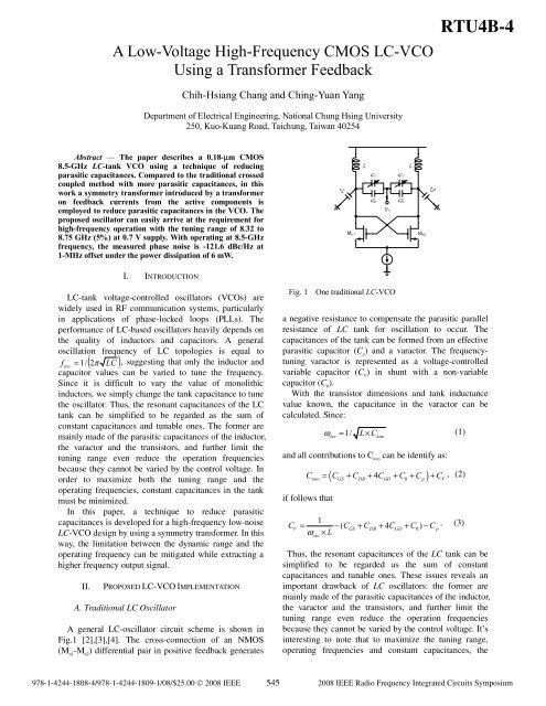
A Low-Voltage High-Frequency CMOS LC-VCO Using a ...
A Low-Voltage High-Frequency CMOS LC-VCO Using a ...
A Low-Voltage High-Frequency CMOS LC-VCO Using a ...

Create successful ePaper yourself
Turn your PDF publications into a flip-book with our unique Google optimized e-Paper software.
A <strong>Low</strong>-<strong>Voltage</strong> <strong>High</strong>-<strong>Frequency</strong> <strong>CMOS</strong> <strong>LC</strong>-<strong>VCO</strong><br />
<strong>Using</strong> a Transformer Feedback<br />
RTU4B-4<br />
Chih-Hsiang Chang and Ching-Yuan Yang<br />
Department of Electrical Engineering, National Chung Hsing University<br />
250, Kuo-Kuang Road, Taichung, Taiwan 40254<br />
Abstract — The paper describes a 0.18-μm <strong>CMOS</strong><br />
8.5-GHz <strong>LC</strong>-tank <strong>VCO</strong> using a technique of reducing<br />
parasitic capacitances. Compared to the traditional crossed<br />
coupled method with more parasitic capacitances, in this<br />
work a symmetry transformer introduced by a transformer<br />
on feedback currents from the active components is<br />
employed to reduce parasitic capacitances in the <strong>VCO</strong>. The<br />
proposed oscillator can easily arrive at the requirement for<br />
high-frequency operation with the tuning range of 8.32 to<br />
8.75 GHz (5%) at 0.7 V supply. With operating at 8.5-GHz<br />
frequency, the measured phase noise is -121.6 dBc/Hz at<br />
1-MHz offset under the power dissipation of 6 mW.<br />
M n1<br />
0 0<br />
Mn2<br />
I. INTRODUCTION<br />
<strong>LC</strong>-tank voltage-controlled oscillators (<strong>VCO</strong>s) are<br />
widely used in RF communication systems, particularly<br />
in applications of phase-locked loops (PLLs). The<br />
performance of <strong>LC</strong>-based oscillators heavily depends on<br />
the quality of inductors and capacitors. A general<br />
oscillation frequency of <strong>LC</strong> topologies is equal to<br />
( 2π<br />
<strong>LC</strong> )<br />
f osc<br />
= 1/ , suggesting that only the inductor and<br />
capacitor values can be varied to tune the frequency.<br />
Since it is difficult to vary the value of monolithic<br />
inductors, we simply change the tank capacitance to tune<br />
the oscillator. Thus, the resonant capacitances of the <strong>LC</strong><br />
tank can be simplified to be regarded as the sum of<br />
constant capacitances and tunable ones. The former are<br />
mainly made of the parasitic capacitances of the inductor,<br />
the varactor and the transistors, and further limit the<br />
tuning range even reduce the operation frequencies<br />
because they cannot be varied by the control voltage. In<br />
order to maximize both the tuning range and the<br />
operating frequencies, constant capacitances in the tank<br />
must be minimized.<br />
In this paper, a technique to reduce parasitic<br />
capacitances is developed for a high-frequency low-noise<br />
<strong>LC</strong>-<strong>VCO</strong> design by using a symmetry transformer. In this<br />
way, the limitation between the dynamic range and the<br />
operating frequency can be mitigated while extracting a<br />
higher frequency output signal.<br />
II.<br />
PROPOSED <strong>LC</strong>-<strong>VCO</strong> IMPLEMENTATION<br />
A. Traditional <strong>LC</strong> Oscillator<br />
A general <strong>LC</strong>-oscillator circuit scheme is shown in<br />
Fig.1 [2],[3],[4]. The cross-connection of an NMOS<br />
(M n1<br />
-M n2<br />
) differential pair in positive feedback generates<br />
Fig. 1 One traditional <strong>LC</strong>-<strong>VCO</strong><br />
a negative resistance to compensate the parasitic parallel<br />
resistance of <strong>LC</strong> tank for oscillation to occur. The<br />
capacitances of the tank can be formed from an effective<br />
parasitic capacitor (C p<br />
) and a varactor. The frequencytuning<br />
varactor is represented as a voltage-controlled<br />
variable capacitor (C V<br />
) in shunt with a non-variable<br />
capacitor (C 0<br />
).<br />
With the transistor dimensions and tank inductance<br />
value known, the capacitance in the varactor can be<br />
calculated. Since:<br />
ω = 1/ L× C<br />
(1)<br />
osc<br />
and all contributions to C toto<br />
can be identify as:<br />
toto<br />
( 4<br />
0 )<br />
C = C + C + C + C + C + C , (2)<br />
if follows that<br />
toto GS DB GD p V<br />
1<br />
C = − ( C + C + 4 C + C ) −C<br />
. (3)<br />
V GS DB GD 0 p<br />
ωosc<br />
× L<br />
Thus, the resonant capacitances of the <strong>LC</strong> tank can be<br />
simplified to be regarded as the sum of constant<br />
capacitances and tunable ones. These issues reveals an<br />
important drawback of <strong>LC</strong> oscillators: the former are<br />
mainly made of the parasitic capacitances of the inductor,<br />
the varactor and the transistors, and further limit the<br />
tuning range even reduce the operation frequencies<br />
because they cannot be varied by the control voltage. It’s<br />
interesting to note that to maximize the tuning range,<br />
operating frequencies and constant capacitances, the<br />
978-1-4244-1808-4/978-1-4244-1809-1/08/$25.00 © 2008 IEEE 545 2008 IEEE Radio <strong>Frequency</strong> Integrated Circuits Symposium
Fig. 3 <strong>LC</strong> oscillation circuit equivalent<br />
Fig. 2 The proposed <strong>LC</strong>-<strong>VCO</strong> with transformer based inductors<br />
constant part in the tank must be minimized. However, it<br />
nevertheless suffers from a trade-off between the<br />
dynamic range and the operating frequency. The parasitic<br />
capacitances from the transistors and varactor constitute<br />
a significant fraction of the overall capacitance, thereby<br />
limiting tuning range [1].<br />
B. Proposed <strong>LC</strong>-<strong>VCO</strong> <strong>Using</strong> a Transformer Based<br />
Inductor<br />
To exclude the effective parasitic capacitor, an<br />
<strong>LC</strong>-based oscillator scheme with a symmetry<br />
transformer-based inductor is shown in Fig. 2. The<br />
symmetry transformer is placed between the gate and<br />
drain of M 1<br />
, the circuit with a feedback loop to oscillate.<br />
In order to reduce the required supply voltage and to<br />
eliminate additional noise contribution, the tail current in<br />
a conventional cross-coupled <strong>VCO</strong> is replaced by a<br />
system inductor L 5<br />
-L 6<br />
. The <strong>LC</strong> oscillation scheme formed<br />
by inductor, the varactor and the transistors but without<br />
effective parasitic capacitor (C p<br />
). The total capacitance<br />
seen from X to ground is equal to C toto<br />
plus the Miller<br />
multiplication of CGS + CDB + 2CGD + C + C , assumed<br />
0 V<br />
A<br />
V<br />
=− 1. Now the varactor capacitance can be calculated.<br />
All contributions to C toto<br />
are identified as:<br />
If follows that<br />
C = C + C + 2C + C + C (4)<br />
toto GS DB GD 0 V<br />
1<br />
C = − C + C + C + C<br />
ω × L<br />
[ 2<br />
0 ]<br />
V DB GD GS<br />
osc<br />
(5)<br />
As expected, total capacitance (C toto<br />
) in (2) is reduced<br />
to (4) for proposed <strong>LC</strong>-<strong>VCO</strong>. The resonant circuit is<br />
generally the type of parallel <strong>LC</strong>-tank, which is formed<br />
by the equivalent inductance from the primary coil of the<br />
transformer and the parasitic capacitances across the<br />
Fig. 4 Half circuit equivalent<br />
port.<br />
III.<br />
SIMPLIFIED LINEAR ANALYSIS<br />
We exploit the <strong>LC</strong> oscillation scheme of Fig. 3 to<br />
construct the equivalent circuit shown in Fig. 2. It is<br />
composed of three mutual inductors L 1<br />
-L 6<br />
[5], a MOS<br />
transistor pair. The inductors possess the coupling factor<br />
K and coupling polarity is assigned by the dot convention<br />
in the figure. The <strong>LC</strong> oscillation operation can be<br />
explained by considering the half-circuit model of Fig. 4.<br />
In the figure, R 1<br />
and L 1<br />
represent the series resistance and<br />
inductance of the primary coil respectively while R 2<br />
and<br />
L 2<br />
represents that of the secondary coil; C is the effective<br />
tank capacitance. In this work, a symmetric structure of<br />
the transformer is adopted, thereby L 1<br />
= L 2<br />
= L, and R 1<br />
=<br />
R 2<br />
= R. By considering the resonator core’s loop in Fig. 4,<br />
we have<br />
1<br />
+ × − × + × = 0 (6)<br />
sC<br />
( sL R) i2 i1 sKL i2<br />
i = g × v<br />
(7)<br />
1 m1<br />
vx<br />
sg<br />
1<br />
=− i2<br />
× (8)<br />
sC<br />
546
Fig. 5 Die photo of the fabricated chip<br />
Fig. 8 Measured output spectrum<br />
<br />
<br />
<br />
<br />
<br />
<br />
<br />
<br />
<br />
<br />
Fig. 6 Measured phase-noise corner<br />
Fig. 9 Measured phase noise<br />
<br />
<br />
<br />
<br />
<br />
<br />
<br />
<br />
<br />
<br />
<br />
<br />
<br />
<br />
<br />
Fig. 7 Measured characteristics of tuning frequency range<br />
ω = (10)<br />
<strong>LC</strong><br />
2 1<br />
osc<br />
The oscillation frequency obviously depends on the<br />
inductances and capacitances of the tank. In addition,<br />
oscillate loss through the serial resistance R will be<br />
cancelled while oscillating. By equations (9) and (10),<br />
the transconductance must satisfy the following<br />
condition for a sustained oscillation:<br />
g<br />
KL<br />
m1<br />
+ gm<br />
1R5<br />
C ≥ R<br />
( 1 )<br />
(11)<br />
Substituting s = jω from above equations, we can get<br />
i<br />
2<br />
<br />
R−<br />
<br />
<br />
gm<br />
1KL<br />
<br />
gm<br />
1R5<br />
C <br />
<br />
( 1+<br />
)<br />
1 <br />
+ jω<br />
L− 0<br />
2 =<br />
ω C <br />
(9)<br />
Imaginary parts of the denominator must drop to zero<br />
when oscillation occurs, and we have<br />
and we get<br />
g<br />
m1<br />
RC<br />
≥<br />
KL−<br />
RCR<br />
IV.<br />
5<br />
(12)<br />
MEASUREMENT RESULTS<br />
To verify the performance of the <strong>LC</strong>-<strong>VCO</strong> as<br />
previously described, the proposed circuits were<br />
fabricated in 0.18-μm <strong>CMOS</strong> technology. Fig. 5 shows<br />
547
the microphotograph of the test chip with an area of<br />
830×910 μm 2 including the output buffers and I/O pads.<br />
Each output signal is connected to an open-drain circuit<br />
with an externally match resistance of 50 Ω. The <strong>VCO</strong><br />
was tested on an FR-4 PC board using Agilent E4407B<br />
Spectrum analyzer for measurement. With a 0.7-V supply,<br />
it consumes the power of 6 mW. Fig. 6 shows the<br />
measured phase noise at 1-MHz offset. The measured<br />
frequency tuning characteristic is shown in Fig. 7. As can<br />
be seen, the tuning range is 5% (8.32 to 8.75 GHz). The<br />
measured spectrum of 8.5 GHz is shown in Fig. 8, and<br />
they prove that the resonant oscillation of the <strong>LC</strong>-tank<br />
merely occurs in the primary of the transformers. Fig. 9<br />
shows a plot of the measured phase noise of the 8.5-GHz<br />
output is -121.5dB/c at 1-MHz offset.<br />
A widely accepted figure of merit (FoM) for <strong>VCO</strong>s is<br />
given by [6]:<br />
f0 Pdiss<br />
<br />
FoM = PN ( Δf<br />
) − 20 log<br />
+ 10 log<br />
(13)<br />
Δf<br />
1mW<br />
<br />
The FoM normalizes the phase noise at a given offset Δf,<br />
the center frequency f 0<br />
, and the power consumption<br />
P in milliwatts. The best FoM of the <strong>VCO</strong> is −190<br />
diss<br />
dBc/Hz. Table 1 shows the FoM of several comparable<br />
under around 1-V supply over the past years [7]-[10].<br />
V. CONCLUSION<br />
A high frequency and low voltage <strong>LC</strong>-<strong>VCO</strong> was<br />
achieved by using a symmetric transformer-based<br />
inductor. It is an interesting work covering the use of<br />
Miller multiplication to reduce parasitic capacitances, for<br />
building high-frequency <strong>VCO</strong>s. The prototype <strong>LC</strong>-<strong>VCO</strong><br />
can extend the operating frequencies at 8.32 to 8.75 GHz<br />
in a standard 0.18-μm <strong>CMOS</strong> process at minimum<br />
operating supply voltages of 0.7 V. The measured results<br />
demonstrate the functionality of the <strong>LC</strong>-<strong>VCO</strong>s with the<br />
proposed to reduce parasitic capacitances technique.<br />
ACKNOWLEDGMENT<br />
The authors would like to thank the National Science<br />
Council, Taiwan, for the financial support and the Chip<br />
Implementation Center (CIC), Taiwan, for the<br />
infrastructure support. This work was sponsored by<br />
NSC95-2220-E- 005-003<br />
REFERENCES<br />
[1] C.Y. Yang and M.T. Tsai, “<strong>High</strong>-frequency low-noise<br />
voltage-controlled <strong>LC</strong>-tank oscillators using a tunable<br />
inductor technique,” IEICE Trans. Electron., Vol. E89-C,<br />
No.11, pp. 1567-1574, Nov. 2006.<br />
[2] K. Andreani and H. Sjoland, “Tail current noise<br />
suppression in RF <strong>CMOS</strong> <strong>VCO</strong>s,” IEEE J. Solid-State<br />
Circuits, Vol. 37, No. 3, pp. 342-348, Mar. 2002.<br />
[3] J. Cranickx, M. Steyart, and H. Miyakawa, “A fully<br />
integrated spiral <strong>LC</strong> <strong>CMOS</strong> <strong>VCO</strong> set with prescaler for<br />
GSM and DCS-1800,” Proc. IEEE Custom Integrated<br />
Circuits Conference (CICC), pp. 403-406, 1997.<br />
[4] B. Razavi, Design of Analog <strong>CMOS</strong> Integrated Circuits,<br />
McGraw-Hill, 2000.<br />
[5] W. Worapishet, “Extended phase noise performance in<br />
mutual negative resistance <strong>CMOS</strong> <strong>LC</strong> oscillator for low<br />
supply voltages,” IEICE Trans. Electron., Vol. E89-C,<br />
No.6, pp. 732-738, Jun. 2006.<br />
[6] P. Kinget, Integrated GHz <strong>Voltage</strong> Controlled<br />
Oscillators, Kluwer Acdemic Publishers, New York<br />
(1999).<br />
[7] S.-H. Lee, Y.-H. Chuang, L.-R. Chi, and J.-F. Lee, “A<br />
<strong>Low</strong>-<strong>Voltage</strong> 2.4GHz <strong>VCO</strong> with 3D Helical Inductors,”<br />
IEEE APCCAS, Dec, 2006.<br />
[8] M. N. El-Gamal et al., “Very low-voltage (0.8 V)<br />
<strong>CMOS</strong> receiver frontend for 5 GHz RF applications,”<br />
Proc. Inst. Elect. Eng.—Circuits, Devices,Syst,, vol. 149,<br />
no. 5/6, pp. 355–362, Oct.–Dec. 2002.<br />
[9] J-A. Hou, C.-P. Chang, J. Su, T.-S. Liou, S.-C. Wong,<br />
Y.-H. Wang, “A low supply voltage <strong>VCO</strong> implemented<br />
by a single common-source 90 nm <strong>CMOS</strong> transistor,”<br />
IEEE Microwave Wireless Component Letter, Vol. 17,<br />
No. 1, pp. 64-66 (2007).<br />
[10] M.-D. Tsai, Y.-H. Cho, H. Wang, “A 5-GHz low phase<br />
noise differential Colpitts <strong>CMOS</strong> <strong>VCO</strong>,” IEEE<br />
Microwave Wireless Component Letter, Vol. 15, No. 5,<br />
pp. 327-329, May 2005.<br />
Table 1 Comparison of performance with prior works<br />
Technology <strong>Frequency</strong><br />
Refs<br />
[μm]<br />
[GHz]<br />
Turing range<br />
[GHz]<br />
VDD<br />
[V]<br />
Power<br />
[mW]<br />
Phase Noise<br />
[dBc/Hz]<br />
FoM<br />
[dBc/Hz]<br />
This work 0.18 <strong>CMOS</strong> 8.5 0.4 0.7 6 -121.6 @ 1MHz -190<br />
[7] 0.18 <strong>CMOS</strong> 2.4 4.4 1 2.6 -116.8 @ 1MHz -180.25<br />
[8] 0.18 <strong>CMOS</strong> 5.8 0.198 0.8 - -100 @ 500KHz -<br />
[9] 0.9 <strong>CMOS</strong> 1.77 0.07 1 6.26 -107 @ 1MHz -163.0<br />
[10] 0.18 <strong>CMOS</strong> 4.8 0.4 1.5 3 -120 @ 1MHz -188.8<br />
548