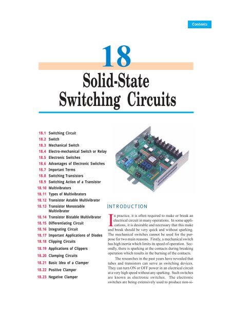
18. Solid-State Switching Circuits - Talking Electronics
18. Solid-State Switching Circuits - Talking Electronics
18. Solid-State Switching Circuits - Talking Electronics

Create successful ePaper yourself
Turn your PDF publications into a flip-book with our unique Google optimized e-Paper software.
468<br />
18<br />
• Principles of <strong>Electronics</strong><br />
<strong>Solid</strong>-<strong>State</strong><br />
<strong>Switching</strong> <strong>Circuits</strong><br />
<strong>18.</strong>1 <strong>Switching</strong> Circuit<br />
<strong>18.</strong>2 Switch<br />
<strong>18.</strong>3 Mechanical Switch<br />
<strong>18.</strong>4 Electro-mechanical Switch or Relay<br />
<strong>18.</strong>5 Electronic Switches<br />
<strong>18.</strong>6 Advantages of Electronic Switches<br />
<strong>18.</strong>7 Important Terms<br />
<strong>18.</strong>8 <strong>Switching</strong> Transistors<br />
<strong>18.</strong>9 <strong>Switching</strong> Action of a Transistor<br />
<strong>18.</strong>10 Multivibrators<br />
<strong>18.</strong>11 Types of Multivibrators<br />
<strong>18.</strong>12 Transistor Astable Multivibrator<br />
<strong>18.</strong>13 Transistor Monostable INTRODUCTION<br />
Multivibrator<br />
<strong>18.</strong>14 Transistor Bistable Multivibrator In practice, it is often required to make or break an<br />
electrical circuit in many operations. In some applications,<br />
it is desirable and necessary that this make<br />
<strong>18.</strong>15 Differentiating Circuit<br />
<strong>18.</strong>16 Integrating Circuit<br />
and break should be very quick and without sparking.<br />
<strong>18.</strong>17 Important Applications of Diodes The mechanical switches cannot be used for the purpose<br />
for two main reasons. Firstly, a mechanical switch<br />
<strong>18.</strong>18 Clipping <strong>Circuits</strong><br />
has high inertia which limits its speed of operation. Secondly,<br />
there is sparking at the contacts during breaking<br />
<strong>18.</strong>19 Applications of Clippers<br />
operation which results in the burning of the contacts.<br />
<strong>18.</strong>20 Clamping <strong>Circuits</strong><br />
The researches in the past years have revealed that<br />
<strong>18.</strong>21 Basic Idea of a Clamper tubes and transistors can serve as switching devices.<br />
They can turn ON or OFF power in an electrical circuit<br />
<strong>18.</strong>22 Positive Clamper<br />
at a very high speed without any sparking. Such switches<br />
<strong>18.</strong>23 Negative Clamper<br />
are known as electronic switches. The electronic<br />
switches are being extensively used to produce non-si-
<strong>Solid</strong>-<strong>State</strong> <strong>Switching</strong> <strong>Circuits</strong> • 469<br />
nusoidal waves e.g., square, rectangular, triangular or saw-tooth waves. <strong>Solid</strong>-state switching circuits<br />
are finding increasing applications. For example, solid-state switching circuits are the fundamental<br />
components of modern computer systems. In this chapter, we shall confine our attention to transistor<br />
as a switch. Once the reader gets acquainted with the switching action of a transistor, he can continue<br />
to study digital electronics on his/her own.<br />
<strong>18.</strong>1 <strong>Switching</strong> Circuit<br />
A circuit which can turn ON or OFF current in an electrical circuit is known as a switching circuit.<br />
A switching circuit essentially consists of two parts viz. (i) a switch and (ii) associated circuitry.<br />
The switch is the most important part of the switching circuit. It actually makes or breaks the electrical<br />
circuit. The function of associated circuitry is to help the switch in turning ON or OFF current in<br />
the circuit. It may be worthwhile to mention here that associated circuitry is particularly used with<br />
electronic switches.<br />
<strong>18.</strong>2 Switch<br />
A switch is a device that can turn ON or OFF current in an electrical circuit. It is the most important<br />
part of a switching circuit. The switches can be broadly classified into the following three types :<br />
(i) Mechanical switch<br />
(ii) Electro-mechanical switch or Relay<br />
(iii) Electronic switch<br />
Although the basic purpose of this chapter is to discuss the switching action of a transistor, yet a<br />
brief description of mechanical and electromechanical switches is being presented. This will help the<br />
reader to understand the importance of transistor as a switch.<br />
<strong>18.</strong>3 Mechanical Switch<br />
A switch which is operated mechanically to turn ON or OFF current in<br />
an electrical circuit is known as a mechanical switch.<br />
The familiar example of a mechanical switch is the tumbler switch<br />
used in homes to turn ON or OFF power supply to various appliances<br />
such as fans, heaters, bulbs etc. The action of a mechanical switch can<br />
Fig. <strong>18.</strong>1<br />
be beautifully understood by referring to Fig. <strong>18.</strong>1 where a load R L<br />
is<br />
connected in series with a battery and a mechanical switch S. As long as the switch is open, there is<br />
no current in the circuit. When switch is closed, the current flow is established in the circuit. It is easy<br />
to see that the whole current flows through the load as well as the switch.<br />
Limitations. A mechanical switch suffers from<br />
the following drawbacks :<br />
(i) In the closed position, the switch carries<br />
the whole of the load current. For a large load current,<br />
the switch contacts have to be made heavy to<br />
enable them to carry the necessary current without<br />
overheating. This increases the size of the switch.<br />
(ii) If the load current carried by the circuit is<br />
large, there will be sparking at the contacts of the<br />
switch during breaking operation. This results in<br />
the wear and tear of the contacts.<br />
(iii) Due to high inertia of a mechanical switch,<br />
the speed of operation is very small.<br />
Mechanical Switches
470 • Principles of <strong>Electronics</strong><br />
Due to above limitations, the use of mechanical switches is restricted to situations where switching<br />
speed is small and the load current to be handled is not very heavy.<br />
<strong>18.</strong>4 Electro-mechanical Switch or Relay<br />
It is a mechanical switch which is operated electrically to turn ON or OFF current in an electrical<br />
circuit.<br />
The electro-mechanical<br />
switch or relay is an improved<br />
form of simple mechanical switch.<br />
Fig. <strong>18.</strong>2 shows the schematic diagram<br />
of a typical relay. It consists<br />
of lever L carrying armature A and<br />
a solenoid C. The spring pulls the<br />
lever upwards while the solenoid<br />
when energised pulls it downwards.<br />
The solenoid circuit is so<br />
designed that when switch S is<br />
closed, the downward pull of the<br />
solenoid exceeds the upward pull<br />
of the spring.<br />
When the switch S is closed,<br />
the lever is pulled downward and<br />
the armature A closes the relay<br />
contacts 1 and 2. This turns ON<br />
current in the circuit. However,<br />
Fig. <strong>18.</strong>2<br />
when switch S is opened, the solenoid<br />
is de-energised and the spring pulls the lever and hence the armature A upwards. Consequently,<br />
the relay contacts 1 and 2 are opened and current flow in the circuit is interrupted. In this<br />
way, a relay acts as a switch.<br />
Advantages. A relay possesses the following advantages over a simple mechanical switch :<br />
(i) The relay or electro-mechanical switch requires a small power for its operation. This permits<br />
to control a large power in the load by a small power to the relay circuit. Thus a relay acts as a<br />
power amplifier i.e. it combines control with power amplification.<br />
(ii) The switch in the relay coil carries a small current as compared to the load current. This<br />
permits the use of a smaller switch in the relay coil circuit.<br />
(iii) The operator can turn ON or OFF power to a load even from a distance. This is a very<br />
important advantage when high voltages are to be handled.<br />
(iv) There is no danger of sparking as the turning ON or OFF is carried by the relay coil switch<br />
which carries a small current.<br />
However, a relay has two principal limitations. First, the speed of operation is very small; less<br />
than 5 operations per second. Secondly, a relay has moving parts and hence there is considerable<br />
wear and tear.<br />
<strong>18.</strong>5 Electronic Switches<br />
It is a device which can turn ON or OFF current in an electrical circuit with the help of electronic<br />
devices e.g., transistors or tubes.
○ ○ ○ ○ ○ ○ ○ ○ ○ ○ ○ ○ ○ ○ ○ ○ ○ ○ ○ ○ ○ ○ ○ ○ ○ ○ ○ ○ ○ ○ ○ ○ ○ ○ ○ ○ ○ ○ ○ ○ ○ ○ ○ ○ ○ ○ ○ ○ ○ ○<br />
<strong>Solid</strong>-<strong>State</strong> <strong>Switching</strong> <strong>Circuits</strong> • 471<br />
Electronic switches have become very popular because of their high speed of operation and<br />
absence of sparking. A transistor can be used as a switch by driving it back and forth between<br />
saturation and cut off. This is illustrated in the discussion below :<br />
Fig. <strong>18.</strong>3<br />
(i) When the base input voltage is enough negative, the transistor is cut off and no current flows<br />
in collector load [See Fig. <strong>18.</strong>3 (i)]. As a result, there is no voltage drop acorss R C<br />
and the output<br />
voltage is *ideally V CC<br />
. i.e.,<br />
I C<br />
= 0 and V CE<br />
= V CC<br />
This condition is similar to that of an open switch (i.e., OFF state) as shown in Fig. <strong>18.</strong>3 (ii).<br />
Fig. <strong>18.</strong>4<br />
(ii) When the input base voltage is positive enough that transistor saturates, then I C(sat)<br />
will flow<br />
through R C<br />
. Under such conditions, the entire V CC<br />
will drop across collector load R C<br />
and output<br />
* The collector current will not be zero since a little leakage current always flows even when the base input<br />
voltage is negative or zero.<br />
∴ Output voltage = V CC<br />
− I leakage<br />
R C<br />
. If I leakage<br />
= 0, then output voltage = V CC<br />
.
472 • Principles of <strong>Electronics</strong><br />
voltage is ideally zero i.e.,<br />
I C<br />
= I C(sat)<br />
=<br />
V<br />
R<br />
CC<br />
C<br />
This condition is similar to that of a closed switch (i.e., ON<br />
state) as shown in Fig. <strong>18.</strong>4 (ii).<br />
Conclusion. The above discussion leads to the conclusion<br />
that a transistor can behave as a switch under proper conditions.<br />
In other words, if the input base voltages are enough negative<br />
and positive, the transistor will be driven between cut off and<br />
saturation. These conditions can be easily fulfilled in a transistor<br />
circuit. Thus a transistor can act as a switch. Fig. <strong>18.</strong>5 shows<br />
the switching action of a transistor in terms of dc load line. The<br />
and V CE<br />
= 0<br />
Fig. <strong>18.</strong>5<br />
Electronic Switches<br />
point A of the load line represents<br />
the ON condition while point B represents<br />
the OFF condition.<br />
Example <strong>18.</strong>1. Determine<br />
the minimum high input voltage<br />
(+V) required to saturate the transistor<br />
switch shown in Fig. <strong>18.</strong>6.<br />
Solution. Assuming the<br />
transistor to be ideal,<br />
I C(sat)<br />
= V CC<br />
/R C<br />
= 10 V/1 k Ω = 10 mA<br />
I Csat<br />
( ) 10 mA<br />
∴ I B<br />
= = = 0.1 mA<br />
β 100<br />
Now<br />
+V = I B<br />
R B<br />
+ V BE<br />
= (0.1 mA) (47 kΩ) + 0.7<br />
= 4.7 + 0.7 = 5.4 V<br />
Fig. <strong>18.</strong>6
○ ○ ○ ○ ○ ○ ○ ○ ○ ○ ○ ○ ○ ○ ○ ○ ○ ○ ○ ○ ○ ○ ○ ○ ○ ○ ○ ○ ○ ○ ○ ○ ○ ○ ○ ○ ○ ○ ○ ○ ○ ○ ○ ○ ○ ○ ○ ○ ○ ○<br />
Hence in order to saturate the transistor, we require + 5.4 V.<br />
<strong>18.</strong>6 Advantages of Electronic Switches<br />
<strong>Solid</strong>-<strong>State</strong> <strong>Switching</strong> <strong>Circuits</strong> • 473<br />
The following are the advantages of transistor switch over other types of switches :<br />
(i) It has no moving parts and hence there is little wear and tear. Therefore, it gives noiseless<br />
operation.<br />
(ii) It has smaller size and weight.<br />
(iii) It gives troublefree service because of solid state.<br />
(iv) It is cheaper than other switches and requires little maintenance.<br />
(v) It has a very fast speed of operation say upto 10 9 operations per second. On the other hand,<br />
the mechanical switches have a small speed of operation e.g. less than 5 operations in a second.<br />
<strong>18.</strong>7. Important Terms<br />
So far we have considered the transistor to be an ideal one. An ideal transistor has V CE<br />
= V CC<br />
(or I C<br />
= 0) in the OFF state and V CE<br />
= 0 (or I C<br />
= I C(sat)<br />
) in the ON state. However, such ideal conditions are<br />
not realised in practice. In a practical transistor, the output voltage is neither V CC<br />
in the OFF state nor<br />
it is zero in the ON state. While designing a transistor<br />
switching circuit, these points must be taken into consideration.<br />
(i) Collector leakage current. When the input circuit<br />
is reverse biased or input voltage is zero, a small<br />
current (a few µA) flows in the collector. This is known<br />
as collector leakage current and is due to the minority<br />
carriers. The value of this leakage current is quite large<br />
in Ge transistors, but in modern silicon transistors, the<br />
value of leakage current is low enough to be ignored.<br />
(ii) Saturation collector current. It is the maximum<br />
collector current for a particular load in a transistor.<br />
Consider an npn transistor having a load R C<br />
in its<br />
collector circuit as shown in Fig. <strong>18.</strong>7. As the input forward bias is increased, the collector current I C<br />
also increases because I C<br />
= βI B<br />
. However, with the increase in I C<br />
, the voltage drop across R C<br />
increases.<br />
This results in the *decrease of V CE<br />
. When V CE<br />
drops to knee voltage (V knee<br />
), any further<br />
increase in collector current is not possible since β decreases sharply when V CE<br />
falls below knee<br />
voltage. This maximum current is known as saturation collector current.<br />
VCC<br />
− Vknee<br />
∴ Saturation collector current, I C (sat)<br />
=<br />
R<br />
Fig. <strong>18.</strong>7<br />
C<br />
<strong>18.</strong>8 <strong>Switching</strong> Transistors<br />
* V CE<br />
= V CC<br />
− I C<br />
R C<br />
A transistor which is used as a switch is known as a switching transistor.<br />
In general, switching transistor is fabricated by the same process as an ordinary transistor except<br />
that it has special design features to reduce switch-off time and saturation voltage. It is so arranged in<br />
the circuit that either maximum current (called saturation collector current) flows through the load or
○ ○ ○ ○ ○ ○ ○ ○ ○ ○ ○ ○ ○ ○ ○ ○ ○ ○ ○ ○ ○ ○ ○ ○ ○ ○ ○ ○ ○ ○ ○ ○ ○ ○ ○ ○ ○ ○ ○ ○ ○ ○ ○ ○ ○ ○ ○ ○ ○ ○<br />
474 • Principles of <strong>Electronics</strong><br />
minimum current (called collector leakage current) flows through the load. In other words, a switching<br />
transistor has two states viz. (i) ON state or when collector saturation current flows through the<br />
load (ii) OFF state or when collector leakage current flows through the load. In the discussion that<br />
follows transistor means the switching transistor.<br />
<strong>18.</strong>9 <strong>Switching</strong> Action of a Transistor<br />
The switching action of a transistor can also be explained with the help of output characteristics. Fig.<br />
<strong>18.</strong>8 shows the output characteristics of a typical transistor for a CE configuration. The load line is<br />
drawn for load R C<br />
and collector supply V CC<br />
. The characteristics are arranged in three regions : OFF,<br />
ON or saturation and active regions.<br />
Fig. <strong>18.</strong>8<br />
(i) OFF region. When the input base voltage is zero or *negative, the transistor is said to be in<br />
the OFF condition. In this condition, I B<br />
= 0 and the collector current is equal to the collector leakage<br />
current I CEO<br />
. The value of I CEO<br />
can be obtained from the characteristics if we know V CE<br />
.<br />
Power loss = Output voltage × Output current<br />
As already noted, in the OFF condition, the output voltage = V CC<br />
since voltage drop in the load<br />
due to I CEO<br />
is negligible.<br />
∴<br />
Power loss = V CC<br />
× I CEO<br />
Since I CEO<br />
is very small as compared to full-load current that flows in the ON condition, power<br />
loss in the transistor is quite small in the OFF condition. It means that the transistor has a high<br />
efficiency as a switch in the OFF condition.<br />
(ii) ON or saturation region. When the input voltage is made so much positive that saturation<br />
collector current flows, the transistor is said to be in the ON condition. In this condition, the saturation<br />
collector current is given by :<br />
VCC<br />
− Vknee<br />
I C(sat)<br />
=<br />
R<br />
C<br />
Power loss = Output voltage × Output current<br />
* If a small negative voltage is given to the input, the base-emitter junction is reverse biased and load current<br />
becomes I CBO<br />
instead of I CEO<br />
.
<strong>Solid</strong>-<strong>State</strong> <strong>Switching</strong> <strong>Circuits</strong> • 475<br />
The output voltage in the ON condition is equal to V knee<br />
and output current is I C(sat)<br />
.<br />
∴<br />
Power loss = V knee<br />
× I C(sat)<br />
Again the efficiency of transistor as a switch in the ON condition is high. It is because the power<br />
loss in this condition is quite low due to small value of V knee<br />
.<br />
(iii) Active region. It is the region that lies between OFF and ON conditions.<br />
The OFF and ON regions are the stable regions of operation. The active region is the unstable<br />
(or transient) region through which the operation of the transistor passes while changing from OFF<br />
state to the ON state. Thus referring to Fig. <strong>18.</strong>8, the path AB is the active region. The collector<br />
current increases from I CEO<br />
to I C(sat)<br />
along the path AB as the transistor is switched ON. However,<br />
when the transistor is switched OFF, the collector current decreases from I C(sat)<br />
to I CEO<br />
along BA.<br />
Conclusions<br />
(a) In the active region, the transistor operates as a linear amplifier where small changes in<br />
input current (ΔI B<br />
) cause relatively large changes in output current (ΔI C<br />
).<br />
(b) In the saturation state, the transistor behaves like a virtual short (collector – emitter shorted),<br />
where V CE<br />
is approximately zero and I C<br />
is maximum, limited only by the resistance R C<br />
in the collector.<br />
In the cut off state, the transistor behaves like an open circuit (collector-emitter open), where I C<br />
is<br />
practically zero and V CE<br />
is equal to supply voltage V CC<br />
. Thus transistor in the saturation and cut<br />
off states behaves as a switch—saturation state corresponds to the closure of switch and cut off state<br />
corresponding to opening of switch.<br />
Note. Transistor switch is inferior to mechanical switch or relay in one respect. When the mechanical<br />
switch or relay is in the OFF condition, the load current is exactly zero. But when transistor switch is in the OFF<br />
condition, the collector current is not zero but is equal to small collector leakage current. However, for all<br />
practical purposes, this small collector leakage current may be neglected.<br />
Example <strong>18.</strong>2. A transistor is used as a switch. If V CC<br />
= 10V, R C<br />
= 1 kΩ and I CBO<br />
= 10 μA,<br />
determine the value of V CE<br />
when the transistor is (i) cut off and (ii) saturated.<br />
Solution.<br />
(i) At cut off<br />
I C<br />
= I CBO<br />
= 10 µA<br />
∴ V CE<br />
= V CC<br />
– I CBO<br />
R C<br />
= 10 V – 10 μA × 1 kΩ = 10V – 10 mV = 9.99V<br />
(ii) At saturation<br />
VCC<br />
− Vknee<br />
I C (sat)<br />
=<br />
RC<br />
∴ V CE<br />
= V knee<br />
= 0.7V<br />
Example <strong>18.</strong>3. Fig. <strong>18.</strong>9 shows the transistor switching circuit. Given that R B<br />
= 2.7 kΩ, V BB<br />
=<br />
2V, V BE<br />
= 0.7V and V knee<br />
= 0.7V.<br />
(i) Calculate the minimum value of β for saturation.<br />
(ii) If V BB<br />
is changed to 1V and transistor has minimum β = 50, will the transistor be saturated.<br />
Solution.<br />
VBB<br />
− VBE<br />
(i) I B<br />
=<br />
RB<br />
2V – 0.7V 1.3 V<br />
= =<br />
2.7 kΩ<br />
2.7 kΩ = 0.48 mA<br />
VCC<br />
− Vknee<br />
Now I C (sat)<br />
=<br />
R<br />
C
○ ○ ○ ○ ○ ○ ○ ○ ○ ○ ○ ○ ○ ○ ○ ○ ○ ○ ○ ○ ○ ○ ○ ○ ○ ○ ○ ○ ○ ○ ○ ○ ○ ○ ○ ○ ○ ○ ○ ○ ○ ○ ○ ○ ○ ○ ○ ○ ○ ○<br />
476 • Principles of <strong>Electronics</strong><br />
Fig. <strong>18.</strong>9<br />
= 10V – 0.7V =<br />
9.3V<br />
1kΩ 1kΩ<br />
= 9.3 mA<br />
∴ Minimum β =<br />
IC( sat) 9.3mA<br />
= = 19.4<br />
IB<br />
0.48 mA<br />
(ii) I B<br />
=<br />
VBB<br />
− VBE<br />
R<br />
B<br />
= 1V – 0.7V =<br />
0.3V<br />
2.7 kΩ 2.7 kΩ<br />
= 0.111 mA<br />
∴ I C<br />
= βI B<br />
= 50 × 0.111 = 5.55 mA<br />
Since the collector current is less than saturation current (= 9.3 mA), the transistor will not be<br />
saturated.<br />
<strong>18.</strong>10 Multivibrators<br />
An electronic circuit that generates square waves (or other non-sinusoidals such as rectangular,<br />
saw-tooth waves) is known as a *multivibrator.<br />
Fig. <strong>18.</strong>10<br />
A multivibrator is a switching circuit which depends for operation on positive feedback. It is<br />
basically a two-stage amplifier with output of one fedback to the input of the other as shown in<br />
Fig. <strong>18.</strong>10.<br />
* The name multivibrator is derived from the fact that a square wave actually consists of a large number of<br />
(fourier series analysis) sinusoidals of different frequencies.
<strong>Solid</strong>-<strong>State</strong> <strong>Switching</strong> <strong>Circuits</strong> • 477<br />
The circuit operates in two states (viz ON and OFF) controlled by circuit conditions. Each amplifier<br />
stage supplies feedback to the other in such a manner that will drive the transistor of one stage to<br />
saturation (ON state) and the other to cut off (OFF state).<br />
After a certain time controlled by circuit conditions,<br />
the action is reversed i.e. saturated stage<br />
is driven to cut off and the cut off stage is driven<br />
to saturation. The output can be taken across either<br />
stage and may be rectangular or square wave<br />
depending upon the circuit conditions.<br />
Fig. <strong>18.</strong>10 shows the block diagram of a<br />
multivibrator. It is a two-stage amplifier with 100%<br />
positive feedback. Suppose output is taken across<br />
the transistor Q 2<br />
. At any particular instant, one<br />
transistor is ON and conducts I C(sat)<br />
while the other<br />
is OFF. Suppose Q 2<br />
is ON and Q 1<br />
is OFF. The<br />
collector current in Q 2<br />
will be I C(sat)<br />
as shown in<br />
Fig. <strong>18.</strong>11<br />
Fig. <strong>18.</strong>11. This condition will prevail for a time (bc in this case) determined by circuit conditions.<br />
After this time, transistor Q 2<br />
is cut off and Q 1<br />
is turned ON. The collector current in Q 2<br />
is now I CEO<br />
as shown. The circuit will stay in this condition for a time de. Again Q 2<br />
is turned ON and Q 1<br />
is driven<br />
to cut off. In this way, the output will be a square wave.<br />
<strong>18.</strong>11 Types of Multivibrators<br />
A multivibrator is basically a two-stage amplifier with output of one fedback to the input of the other.<br />
At any particular instant, one transistor is ON and the other is OFF. After a certain time depending<br />
upon the circuit components, the stages reverse their conditions – the conducting stage suddenly cuts<br />
off and the non-conducting stage suddenly starts to conduct. The two possible states of a multivibrator<br />
are :<br />
ON<br />
OFF<br />
First <strong>State</strong> Q 1<br />
Q 2<br />
Second <strong>State</strong> Q 2<br />
Q 1<br />
Depending upon the manner in which the two stages interchange their states, the multivibrators<br />
are classified as :<br />
(i) Astable or free running multivibrator<br />
(ii) Monostable or one-shot multivibrator<br />
(iii) Bi-stable or flip-flop multivibrator<br />
Fig. <strong>18.</strong>12 shows the input/output relations for the three types of multivibrators.<br />
(i) The astable or free running multivibrator alternates automatically between the two states<br />
and remains in each for a time dependent upon the circuit constants. Thus it is just an oscillator since<br />
it requires no external pulse for its operation. Of course, it does require a source of d.c. power.<br />
Because it continuously produces the square-wave output, it is often referred to as a free running<br />
multivibrator.<br />
(ii) The monostable or one-shot multivibrator has one state stable and one quasi-stable (i.e.<br />
half-stable) state. The application of input pulse triggers the circuit into its quasi-stable state, in<br />
which it remains for a period determined by circuit constants. After this period of time, the circuit<br />
returns to its initial stable state, the process is repeated upon the application of each trigger pulse.<br />
Since the monostable multivibrator produces a single output pulse for each input trigger pulse, it is<br />
generally called one-shot multivibrator.
○ ○ ○ ○ ○ ○ ○ ○ ○ ○ ○ ○ ○ ○ ○ ○ ○ ○ ○ ○ ○ ○ ○ ○ ○ ○ ○ ○ ○ ○ ○ ○ ○ ○ ○ ○ ○ ○ ○ ○ ○ ○ ○ ○ ○ ○ ○ ○ ○ ○<br />
478 • Principles of <strong>Electronics</strong><br />
Fig. <strong>18.</strong>12<br />
(iii) The bistable multivibrator has both the two states stable. It requires the application of an<br />
external triggering pulse to change the operation from either one state to the other. Thus one pulse is<br />
used to generate half-cycle of square wave and another pulse to generate the next half-cycle of square<br />
wave. It is also known as a flip-flop multivibrator because of the two possible states it can assume.<br />
<strong>18.</strong>12 Transistor Astable Multivibrator<br />
A multivibrator which generates square waves of its own (i.e. without any external triggering pulse)<br />
is known as an astable or free running multivibrator.<br />
The *astable multivibrator has no stable state. It switches back and forth from one state to the<br />
other, remaining in each state for a time determined by circuit constants. In other words, at first one<br />
transistor conducts (i.e. ON state) and the other stays in the OFF state for some time. After this period<br />
of time, the second transistor is automatically turned ON and the first transistor is turned OFF. Thus<br />
the multivibrator will generate a square wave output of its own. The width of the square wave and its<br />
frequency will depend upon the circuit constants.<br />
Circuit details. Fig. <strong>18.</strong>13 shows the circuit of a typical transistor astable multivibrator using<br />
two identical transistors Q 1<br />
and Q 2<br />
. The circuit essentially consists of two symmetrical CE amplifier<br />
stages, each providing a feedback to the other. Thus collector loads of the two stages are equal i.e.<br />
R 1<br />
= R 4<br />
and the biasing resistors are also equal i.e. R 2<br />
= R 3<br />
. The output of transistor Q 1<br />
is coupled to<br />
the input of Q 2<br />
through C 1<br />
while the output of Q 2<br />
is fed to the input of Q 1<br />
through C 2<br />
. The square<br />
wave output can be taken from Q 1<br />
or Q 2<br />
.<br />
Operation. When V CC<br />
is applied, collector currents start flowing in Q 1<br />
and Q 2<br />
. In addition, the<br />
coupling capacitors C 1<br />
and C 2<br />
also start charging up. As the characteristics of no two transistors<br />
(i.e. β, V BE<br />
) are exactly alike, therefore, one transistor, say Q 1<br />
, will conduct more rapidly than the<br />
other. The rising collector current in Q 1<br />
drives its collector more and more positive. The increasing<br />
positive output at point A is applied to the base of transistor Q 2<br />
through C 1<br />
. This establishes a reverse<br />
* A means not. Hence astable means that it has no stable state.
<strong>Solid</strong>-<strong>State</strong> <strong>Switching</strong> <strong>Circuits</strong> • 479<br />
Fig. <strong>18.</strong>13<br />
bias on Q 2<br />
and its collector current starts decreasing.<br />
As the collector of Q 2<br />
is connected to the base of Q 1<br />
through C 2<br />
, therefore, base of Q 1<br />
becomes more negative<br />
i.e. Q 1<br />
is more forward biased. This further increases<br />
the collector current in Q 1<br />
and causes a further<br />
decrease of collector current in Q 2<br />
. This series of actions<br />
is repeated until the circuit drives Q 1<br />
to saturation<br />
and Q 2<br />
to cut off. These actions occur very rapidly<br />
and may be considered practically instantaneous.<br />
The output of Q 1<br />
(ON state) is approximately zero and<br />
Fig. <strong>18.</strong>14<br />
that of Q 2<br />
(OFF state) is approximately V CC<br />
. This is<br />
shown by ab in Fig. <strong>18.</strong>14.<br />
When Q 1<br />
is at saturation and Q 2<br />
is cut off, the full voltage V CC<br />
appears across R 1<br />
and voltage<br />
across R 4<br />
will be zero. The charges developed across C 1<br />
and C 2<br />
are sufficient to maintain the saturation<br />
and cut off conditions at Q 1<br />
and Q 2<br />
respectively. This condition is represented by time interval bc<br />
in Fig. <strong>18.</strong>14. However, the capacitors will not retain the charges indefinitely but will discharge<br />
through their respective circuits. The discharge path for C 1<br />
, with plate L negative and Q 1<br />
conducting,<br />
is LAQ 1<br />
V CC<br />
R 2<br />
M as shown in Fig. <strong>18.</strong>15 (i).<br />
The discharge path for C 2<br />
, with plate K negative and Q 2<br />
cut off, is KBR 4<br />
R 3<br />
J as shown in Fig.<br />
<strong>18.</strong>15 (ii). As the resistance of the discharge path for C 1<br />
is lower than that of C 2<br />
, therefore, C 1<br />
will<br />
discharge more rapidly.<br />
As C 1<br />
discharges, the base bias at Q 2<br />
becomes less positive and at a time determined by R 2<br />
and<br />
C 1<br />
, forward bias is re-established at Q 2<br />
. This causes the collector current to start in Q 2<br />
. The increasing<br />
positive potential at collector of Q 2<br />
is applied to the base of Q 1<br />
through the capacitor C 2<br />
. Hence<br />
the base of Q 1<br />
will become more positive i.e. Q 1<br />
is reverse biased. The decrease in collector current<br />
in Q 1<br />
sends a negative voltage to the base of Q 2<br />
through C 1<br />
, thereby causing further increase in the<br />
collector current of Q 2<br />
. With this set of actions taking place, Q 2<br />
is quickly driven to saturation and Q 1<br />
to cut off. This condition is represented by cd in Fig. <strong>18.</strong>14. The period of time during which Q 2<br />
remains at saturation and Q 1<br />
at cut off is determined by C 2<br />
and R 3<br />
.
480 • Principles of <strong>Electronics</strong><br />
Fig. <strong>18.</strong>15<br />
ON or OFF time. The time for which either transistor remains ON or OFF is given by :<br />
ON time for Q 1<br />
(or OFF time for Q 2<br />
) is<br />
T 1<br />
= 0.694 R 2<br />
C 1<br />
OFF time for Q 1<br />
(or ON time for Q 2<br />
) is<br />
T 2<br />
= 0.694 R 3<br />
C 2<br />
Total time period of the square wave is<br />
T = T 1<br />
+ T 2<br />
= 0.694 (R 2<br />
C 1<br />
+ R 3<br />
C 2<br />
)<br />
As R 2<br />
= R 3<br />
= R and C 1<br />
= C 2<br />
= C,<br />
∴<br />
T = 0.694 (RC + RC) j 1.4 RC seconds<br />
Frequency of the square wave is<br />
f = 1 g; 0.7 Hz<br />
T RC<br />
It may be noted that in these expressions, R is in ohms and C in farad.<br />
Example <strong>18.</strong>4. In the astable multivibrator shown in Fig. <strong>18.</strong>13, R 2<br />
= R 3<br />
= 10 kΩ and C 1<br />
= C 2<br />
= 0.01 µF. Determine the time period and frequency of the square wave.<br />
Solution.<br />
Here R = 10 kΩ = 10 4 Ω; C = 0.01 µF = 10 −8 F<br />
Time period of the square wave is<br />
T = 1.4 RC = 1.4 × 10 4 × 10 −8 second<br />
= 1.4 × 10 −4 second = 1.4 × 10 −4 × 10 3 m sec<br />
= 0.14 m sec<br />
Frequency of the square wave is<br />
f =<br />
1<br />
Hz =<br />
1<br />
Hz<br />
T in second<br />
−4<br />
1.4 × 10<br />
= 7 × 10 3 Hz = 7 kHz<br />
<strong>18.</strong>13 Transistor Monostable Multivibrator<br />
A multivibrator in which one transistor is always conducting (i.e. in the ON state) and the other is<br />
non-conducting (i.e. in the OFF state) is called a monostable multivibrator.
○ ○ ○ ○ ○ ○ ○ ○ ○ ○ ○ ○ ○ ○ ○ ○ ○ ○ ○ ○ ○ ○ ○ ○ ○ ○ ○ ○ ○ ○ ○ ○ ○ ○ ○ ○ ○ ○ ○ ○ ○ ○ ○ ○ ○ ○ ○ ○ ○ ○<br />
<strong>Solid</strong>-<strong>State</strong> <strong>Switching</strong> <strong>Circuits</strong> • 481<br />
A *monostable multivibrator has only one state stable. In other words, if one transistor is conducting<br />
and the other is non-conducting, the circuit will remain in this position. It is only with the<br />
application of external pulse that the circuit will interchange the states. However, after a certain time,<br />
the circuit will automatically switch back to the original stable state and remains there until another<br />
pulse is applied. Thus a monostable multivibrator cannot generate square waves of its own like an<br />
astable multivibrator. Only external pulse will cause it to generate the square wave.<br />
Circuit details. Fig. <strong>18.</strong>16 shows the circuit of a transistor monostable multivibrator. It consists<br />
of two similar transistors Q 1<br />
and Q 2<br />
with equal collector loads i.e. R 1<br />
= R 4<br />
. The values of V BB<br />
and R 5<br />
are such as to reverse bias Q 1<br />
and keep it at cut off. The collector supply V CC<br />
and R 2<br />
forward bias Q 2<br />
and keep it at saturation. The input pulse is given through C 2<br />
to obtain the square wave. Again output<br />
can be taken from Q 1<br />
or Q 2<br />
.<br />
Fig. <strong>18.</strong>16<br />
Operation. With the circuit arrangement<br />
shown, Q 1<br />
is at cut off and Q 2<br />
is at saturation.<br />
This is the stable state for the circuit and it will<br />
continue to stay in this state until a triggering pulse<br />
is applied at C 2<br />
. When a negative pulse of short<br />
duration and sufficient magnitude is applied to<br />
the base of Q 1<br />
through C 2<br />
, the transistor Q 1<br />
starts<br />
conducting and positive potential is established<br />
at its collector. The positive potential at the collector<br />
of Q 1<br />
is coupled to the base of Q 2<br />
through<br />
capacitor C 1<br />
. This decreases the forward bias on<br />
Q 2<br />
and its collector current decreases. The increasing<br />
negative potential on the collector of Q 2<br />
is<br />
applied to the base of Q 1<br />
through R 3<br />
. This further<br />
increases the forward bias on Q 1<br />
and hence its<br />
collector current. With this set of actions taking<br />
place, Q 1<br />
is quickly driven to saturation and Q 2<br />
to<br />
cut off.<br />
Monostable Multivibrator<br />
* Mono means single.
482 • Principles of <strong>Electronics</strong><br />
With Q 1<br />
at saturation and Q 2<br />
at cut off, the circuit will come back to the original stage (i.e. Q 2<br />
at<br />
saturation and Q 1<br />
at cut off) after some time as explained in the following discussion. The capacitor<br />
C 1<br />
(charged to approximately V CC<br />
) discharges through the path R 2<br />
V CC<br />
Q 1<br />
. As C 1<br />
discharges, it sends<br />
a voltage to the base of Q 2<br />
to make it less positive. This goes on until a point is reached when forward<br />
bias is re-established on Q 2<br />
and collector current starts to flow in Q 2<br />
. The step by step events already<br />
explained occur and Q 2<br />
is quickly driven to saturation and Q 1<br />
to cut off. This is the stable state for the<br />
circuit and it remains in this condition until another pulse causes the circuit to switch over the states.<br />
<strong>18.</strong>14 Transistor Bistable Multivibrator<br />
A multivibrator which has both the states stable is called a bistable multivibrator.<br />
The bistable multivibrator has both the states stable. It will remain in whichever state it happens<br />
to be until a trigger pulse causes it to switch to the other state. For instance, suppose at any particular<br />
instant, transistor Q 1<br />
is conducting and transistor Q 2<br />
is at cut off. If left to itself, the bistable multivibrator<br />
will stay in this position forever. However, if an external pulse is applied to the circuit in such a way<br />
that Q 1<br />
is cut off and Q 2<br />
is turned on, the circuit will stay in the new position. Another trigger pulse<br />
is then required to switch the circuit back to its original state.<br />
Circuit details. Fig. <strong>18.</strong>17 shows the circuit of a typical transistor bistable multivibrator. It<br />
consists of two identical CE amplifier stages with output of one fed to the input of the other. The<br />
feedback is coupled through resistors (R 2<br />
, R 3<br />
) shunted by capacitors C 1<br />
and C 2<br />
. The main purpose of<br />
capacitors C 1<br />
and C 2<br />
is to improve the switching characteristics of the circuit by passing the high<br />
frequency components of the square wave. This allows fast rise and fall times and hence distortionless<br />
square wave output. The output can be taken across either transistor.<br />
Fig. <strong>18.</strong>17<br />
Operation. When V CC<br />
is applied, one transistor will start conducting slightly ahead of the other<br />
due to some differences in the characteristics of the transistors. This will drive one transistor to
<strong>Solid</strong>-<strong>State</strong> <strong>Switching</strong> <strong>Circuits</strong> • 483<br />
saturation and the other to cut off in a manner described for the astable multivibrator. Assume that Q 1<br />
is turned ON and Q 2<br />
is cut OFF. If left to itself, the circuit will stay in this condition. In order to<br />
switch the multivibrator to its other state, a trigger pulse must be applied. A negative pulse applied to<br />
the base of Q 1<br />
through C 3<br />
will cut it off or a positive pulse applied to the base of Q 2<br />
through C 4<br />
will<br />
cause it to conduct.<br />
Suppose a negative pulse of sufficient magnitude is applied to the base of Q 1<br />
through C 3<br />
. This<br />
will reduce the forward bias on Q 1<br />
and cause a decrease in its collector current and an increase in<br />
collector voltage. The rising collector voltage is coupled to the base of Q 2<br />
where it forward biases the<br />
base-emitter junction of Q 2<br />
. This will cause an increase in its collector current and decrease in<br />
collector voltage. The decreasing collector voltage is applied to the base of Q 1<br />
where it further<br />
reverse biases the base-emitter junction of Q 1<br />
to decrease its collector current. With this set of actions<br />
taking place, Q 2<br />
is quickly driven to saturation and Q 1<br />
to cut off. The circuit will now remain stable in<br />
this state until a negative trigger pulse at Q 2<br />
(or a positive trigger pulse at Q 1<br />
) changes this state.<br />
<strong>18.</strong>15 Differentiating Circuit<br />
A circuit in which output voltage is directly proportional to the derivative of the input is known as a<br />
differentiating circuit.<br />
Output ∝<br />
d dt (Input)<br />
A differentiating circuit is a simple RC series circuit with output taken across the resistor R. The<br />
circuit is suitably designed so that output is proportional to the derivative of the input. Thus if a d.c.<br />
or constant input is applied to such a circuit, the output will be zero. It is because the derivative of a<br />
constant is zero.<br />
Fig. <strong>18.</strong>18<br />
Fig. <strong>18.</strong>18 shows a typical differentiating circuit. The output across R will be the derivative of<br />
the input. It is important to note that merely using voltage across R does not make the circuit a<br />
differentiator; it is also necessary to set the proper circuit values. In order to achieve good differentiation,<br />
the following two conditions should be satisfied :<br />
(i) The time constant RC of the circuit should be much smaller than the time period of the input<br />
wave.<br />
(ii) The value of X C<br />
should be 10 or more times larger than R at the operating frequency.<br />
Fulfilled these conditions, the output across R in Fig. <strong>18.</strong>18 will be the derivative of the input.<br />
Let e i<br />
be the input alternating voltage and let i be the resulting alternating current. The charge q<br />
on the capacitor at any instant is<br />
q = C e c<br />
dq<br />
Now i = =<br />
d<br />
() q =<br />
d<br />
( Cec)<br />
dt dt dt
484 • Principles of <strong>Electronics</strong><br />
or i = C<br />
d<br />
( ec)<br />
dt<br />
Since the capacitive reactance is very much larger than R, the input voltage can be considered<br />
equal to the capacitor voltage with negligible error i.e. e c<br />
= e i<br />
.<br />
∴ i = C<br />
d<br />
( e i<br />
)<br />
dt<br />
Output voltage, e o<br />
= i R<br />
= RC<br />
d<br />
( e i<br />
)<br />
dt<br />
d<br />
∝ ( ei )<br />
dt<br />
(ä RC is constant)<br />
∴ Output voltage ∝ d (Input)<br />
dt<br />
Output waveforms. The output waveform from a differentiating circuit depends upon the time<br />
constant and shape of the input wave. Three important cases will be considered.<br />
(i) When input is a square wave. When the input fed to a differentiating circuit is a square<br />
wave, output will consist of sharp narrow pulses as shown in Fig. <strong>18.</strong>19. During the OC part of input<br />
wave, its amplitude changes abruptly and hence the differentiated wave will be a sharp narrow pulse<br />
as shown in Fig. <strong>18.</strong>19. However, during the constant part CB of the input, the output will be zero<br />
because the derivative of a constant is zero.<br />
Fig. <strong>18.</strong>19<br />
Let us look at the physical explanation of this behaviour of the circuit. Since time constant RC of<br />
the circuit is very small w.r.t. time period of input wave and X C<br />
>> R, the capacitor will become fully<br />
charged during the early part of each half-cycle of the input wave. During the remainder part of the<br />
half-cycle, the output of the circuit will be zero because the capacitor<br />
voltage (e c<br />
) neutralises the input voltage and there can be<br />
no current flow through R. Thus we shall get sharp pulse at the<br />
output during the start of each half-cycle of input wave while for<br />
the remainder part of the half-cycle of input wave, the output will<br />
be zero. In this way, a symmetrical output wave with sharp positive<br />
and negative peaks is produced. Such pulses are used in<br />
many ways in electronic circuits e.g. in television transmitters<br />
and receivers, in multivibrators to initiate action etc.<br />
(ii) When input is a triangular wave. When the input fed<br />
to a differentiating circuit is a triangular wave, the output will be<br />
a rectangular wave as shown in Fig. <strong>18.</strong>20. During the period OA<br />
Fig. <strong>18.</strong>20
<strong>Solid</strong>-<strong>State</strong> <strong>Switching</strong> <strong>Circuits</strong> • 485<br />
of the input wave, its amplitude changes at a constant rate and, therefore, the differentiated wave has<br />
a constant value for each constant rate of change. During the period AB of the input wave, the change<br />
is less abrupt so that the output will be a very narrow pulse of rectangular form. Thus when a triangular<br />
wave is fed to a differentiating circuit, the output consists of a succession of rectangular waves of<br />
equal or unequal duration depending upon the shape of the input wave.<br />
(iii) When input is a sine wave. A sine wave input becomes a cosine wave and a cosine wave<br />
input becomes an inverted sine wave at the output.<br />
Example <strong>18.</strong>5. (i) What is the effect of time constant of an RC circuit on the differentiated wave<br />
(ii) Sketch the output waveform from the differentiating circuit when input is square wave for<br />
T = 100 RC, T = 10 RC, T = RC.<br />
Solution.<br />
(i) In an RC differentiating circuit, the output voltage is taken across R and the waveform of the<br />
output depends upon the time constant of the circuit. The circuit will function as a differentiator if the<br />
product RC is many times smaller than the time period of the input wave.<br />
(ii) Square wave input. Fig. <strong>18.</strong>21 shows the input square wave fed to a differentiating circuit.<br />
Fig. <strong>18.</strong>22 shows the output waveforms for different values of time period of the input wave.<br />
Fig. <strong>18.</strong>21<br />
It may be noted that RC coupling circuit is the same as a differentiating circuit except that it has<br />
a long time constant—in excess of 5 RC. Therefore, a coupling circuit does not noticeably differentiate<br />
the input wave.<br />
Fig. <strong>18.</strong>22<br />
Example <strong>18.</strong>6. In a differentiating circuit, R = 10 kΩ and C = 2.2 µF. If the input voltage goes<br />
from 0 V to 10 V at a constant rate in 0.4 s, determine the output voltage.<br />
Solution.<br />
dei<br />
e o<br />
= RC<br />
d<br />
( ei<br />
) = RC<br />
... See Art. <strong>18.</strong>15<br />
dt<br />
dt<br />
de 10 0<br />
Here R = 10 kΩ ; C = 2.2 µF ; i −<br />
= = 25 V/s<br />
dt 0.4<br />
∴ e o<br />
= (10 × 10 3 ) × (2.2 × 10 −6 ) × 25 = 0.55 V
486 • Principles of <strong>Electronics</strong><br />
<strong>18.</strong>16 Integrating Circuit<br />
A circuit in which output voltage is directly proportional to the integral of the input is known as an<br />
integrating circuit i.e.<br />
Output ∝ ∫ Input<br />
An integrating circuit is a simple RC series circuit with output taken across the capacitor C as<br />
shown in Fig. <strong>18.</strong>23. It may be seen that R and C of the differentiating circuit have changed places. In<br />
order that the circuit renders good integration, the following conditions should be fulfilled :<br />
Fig. <strong>18.</strong>23<br />
(i) The time constant RC of the circuit should be very large as compared to the time period of<br />
the input wave.<br />
(ii) The value of R should be 10 or more times larger than X C<br />
.<br />
Let e i<br />
be the input alternating voltage and let i be the resulting alternating current. Since R is very<br />
large as compared to capacitive reactance X C<br />
of the capacitor, it is reasonable to assume that voltage<br />
across R (i.e. e R<br />
) is equal to the input voltage i.e.<br />
e i<br />
= e R<br />
e<br />
Now i = R<br />
e<br />
= i<br />
R R<br />
The charge q on the capacitor at any instant is<br />
q = ∫ idt<br />
Output voltage, e o<br />
=<br />
=<br />
q<br />
C<br />
ei<br />
∫ dt<br />
R<br />
C<br />
idt<br />
= ∫<br />
C<br />
⎛<br />
⎜Q<br />
⎝<br />
i<br />
ei<br />
⎞<br />
=<br />
R ⎟<br />
⎠<br />
=<br />
1<br />
ei<br />
dt<br />
RC ∫<br />
∝ ∫ ei<br />
dt<br />
(ä RC is constant)<br />
∴ Output voltage ∝ ∫ Input<br />
Output waveforms. The output waveform from an integrating circuit depends upon time constant<br />
and shape of the input wave. Two important cases will be discussed :<br />
(i) When input is a square wave. When the input fed to an integrating circuit is a square<br />
wave, the output will be a triangular wave as shown in Fig. <strong>18.</strong>24 (i). As integration means summation,<br />
therefore, output from an integrating circuit will be the sum of all the input waves at any instant.<br />
This sum is zero at A and goes on increasing till it becomes maximum at C. After this, the summation<br />
goes on decreasing to the onset of negative movement CD of the input.
<strong>Solid</strong>-<strong>State</strong> <strong>Switching</strong> <strong>Circuits</strong> • 487<br />
Fig. <strong>18.</strong>24<br />
(ii) When input is rectangular wave. When the input fed to an integrating circuit is a rectangular<br />
wave, the output will be a triangular wave as shown in Fig. <strong>18.</strong>24 (ii).<br />
<strong>18.</strong>17 Important Applications of Diodes<br />
We have seen that diodes can be used as rectifiers. Apart from this, diodes have many other applications.<br />
However, we shall confine ourselves to the following two applications of diodes :<br />
(i) as a clipper (ii) as a clamper<br />
A clipper (or limiter) is used to clip off or remove a portion of an a.c. signal. The half-wave<br />
rectifier is basically a clipper that eliminates one of the alternations of an a.c. signal.<br />
A clamper (or dc restorer) is used to restore or change the dc reference of an ac signal. For<br />
example, you may have a 10 V pp<br />
ac signal that varies equally above and below 2 V dc.<br />
<strong>18.</strong>18 Clipping <strong>Circuits</strong><br />
The circuit with which the waveform is shaped by removing (or clipping) a portion of the applied<br />
wave is known as a clipping circuit.<br />
Clippers find extensive use in radar, digital and other electronic systems. Although several clipping<br />
circuits have been developed to change the wave shape, we shall confine our attention to diode<br />
clippers. These clippers can remove signal voltages above or below a specified level. The important<br />
diode clippers are (i) positive clipper (ii) biased clipper (iii) combination clipper.<br />
(i) Positive clipper. A positive clipper is that which removes the positive half-cycles of the<br />
input voltage. Fig. <strong>18.</strong>25 shows the typical circuit of a positive clipper using a diode. As shown, the<br />
output voltage has all the positive half-cycles removed or clipped off.<br />
Fig. <strong>18.</strong>25
488 • Principles of <strong>Electronics</strong><br />
The circuit action is as follows. During the positive half-cycle of the input voltage, the diode is<br />
forward biased and conducts heavily. Therefore, the voltage across the diode (which behaves as a short)<br />
and hence across the load R L<br />
is zero. Hence *output voltage during positive half-cycles is zero.<br />
During the negative half-cycle of the input voltage, the diode is reverse biased and behaves as an<br />
open. In this condition, the circuit behaves as a voltage divider with an output given by :<br />
RL<br />
Output voltage = − Vm<br />
R + R<br />
L<br />
Generally, R L<br />
is much greater than R.<br />
∴<br />
Output voltage = − V m<br />
It may be noted that if it is desired to remove the negative half-cycle of the input, the only thing<br />
to be done is to reverse the polarities of the diode in the circuit shown in Fig. <strong>18.</strong>25. Such a clipper is<br />
then called a negative clipper.<br />
(ii) Biased clipper. Sometimes it is desired to remove a small portion of positive or negative<br />
half-cycle of the signal voltage. For this purpose, biased clipper is used. Fig. <strong>18.</strong>26 shows the circuit<br />
of a biased clipper using a diode with a battery of V volts. With the polarities of battery shown, a<br />
portion of each positive half-cycle will be clipped. However, the negative half-cycles will appear as<br />
such across the load. Such a clipper is called biased positive clipper.<br />
The circuit action is as follows. The diode will conduct heavily so long as input voltage is greater<br />
than +V. When input voltage is greater than +V, the diode behaves as a short and the output equals +V.<br />
The output will stay at +V so long as the input voltage is greater than +V. During the period the input<br />
voltage is less than +V, the diode is reverse biased and behaves as an open. Therefore, most of the<br />
input voltage appears across the output. In this way, the biased positive clipper removes input voltage<br />
above +V.<br />
During the negative half-cycle of the input voltage, the diode remains reverse biased. Therefore,<br />
almost entire negative half-cycle appears across the load.<br />
Fig. <strong>18.</strong>26<br />
If it is desired to clip a portion of negative half-cycles of input voltage, the only thing to be done<br />
is to reverse the polarities of diode or battery. Such a circuit is then called a biased negative clipper.<br />
(iii) Combination clipper. It is a combination of biased positive and negative clippers. With a<br />
combination clipper, a portion of both positive and negative half-cycles of input voltage can be removed<br />
or clipped as shown in Fig. <strong>18.</strong>27.<br />
Fig. <strong>18.</strong>27<br />
○ ○ ○ ○ ○ ○ ○ ○ ○ ○ ○ ○ ○ ○ ○ ○ ○ ○ ○ ○ ○ ○ ○ ○ ○ ○ ○ ○ ○ ○ ○ ○ ○ ○ ○ ○ ○ ○ ○ ○ ○ ○ ○ ○ ○ ○ ○ ○ ○<br />
○<br />
* It may be noted that all the input voltage during this half-cycle is dropped across R.
<strong>Solid</strong>-<strong>State</strong> <strong>Switching</strong> <strong>Circuits</strong> • 489<br />
The circuit action is as follows. When positive input voltage is greater than +V 1<br />
, diode<br />
D 1<br />
conducts heavily while diode D 2<br />
remains reverse biased. Therefore, a voltage +V 1<br />
appears across<br />
the load. This output stays at +V 1<br />
so long as the input voltage exceeds +V 1<br />
. On the other hand,<br />
during the negative half-cycle, the diode D 2<br />
will conduct heavily and the output stays at −V 2<br />
so<br />
long as the input voltage is greater than −V 2<br />
. Note that +V 1<br />
and −V 2<br />
are less than + V m<br />
and − V m<br />
respectively.<br />
Between +V 1<br />
and −V 2<br />
neither diode is on. Therefore, in this condition, most of the input voltage<br />
appears across the load. It is interesting to note that this clipping circuit can give square wave output<br />
if V m<br />
is much greater than the clipping levels.<br />
Example <strong>18.</strong>7. For the negative series clipper shown in Fig.<strong>18.</strong>28, what is the peak output<br />
voltage from the circuit <br />
Solution. When the diode is connected in series with the load, it is called a series clipper. Since<br />
it is a negative clipper, it will remove negative portion of input a.c. signal.<br />
Fig. <strong>18.</strong>28<br />
During the positive half-cycle of input signal, the dioide is forward biased. As a result, the diode<br />
will conduct. The output voltage is<br />
V out (peak)<br />
= V in (peak)<br />
− 0.7 = 12 − 0.7 = 11.3 V<br />
During the negative half-cycle of input signal, the diode is reverse biased and consequently it<br />
will not conduct. Therefore, V out<br />
= 0. Note that under this condition, the entire input voltage will<br />
appear across the diode.<br />
Example <strong>18.</strong>8. The negative shunt clipper shown in Fig. <strong>18.</strong>29 (i) has a peak input voltage of<br />
+ 10 V. What is the peak output voltage from this circuit <br />
Fig. <strong>18.</strong>29<br />
Solution. When the diode is connected in parallel with the load, it is called a shunt clipper.<br />
During the positive half-cycle of input ac signal, the diode is reverse biased and it will behave as an<br />
open. This is shown in Fig. <strong>18.</strong>29 (ii). With diode as an open,<br />
V out (peak)<br />
= Peak voltage across R L<br />
RL<br />
4<br />
= Vin<br />
( peak)<br />
= × 10 = 8V<br />
R + R<br />
1+<br />
4<br />
Note that peak output voltage is somewhat less than the peak input voltage.<br />
L
490 • Principles of <strong>Electronics</strong><br />
Example <strong>18.</strong>9. In example <strong>18.</strong>8, what will be the output voltage and voltage across R when the<br />
input voltage is −10 V <br />
Solution. During the negative half-cycle of input signal, the diode is forward biased. Therefore,<br />
diode can be replaced by its simplified equivalent circuit as shown in Fig. <strong>18.</strong>30. Since load is<br />
connected in parallel with the diode,<br />
Fig. <strong>18.</strong>30<br />
∴ V out<br />
= − 0.7 V<br />
Voltage across R, V R<br />
= (− 10) − (− 0.7) = − 10 + 0.7 = − 9.3 V<br />
Example <strong>18.</strong>10. The positive shunt clipper shown in Fig. <strong>18.</strong>31 has the input waveform as<br />
indicated. Determine the value of V out<br />
for each of the input alternations.<br />
Fig. <strong>18.</strong>31<br />
Solution.<br />
Positive half-cycle. During the positive half-cycle of the input ac signal, the diode is forward<br />
biased. Therefore, diode can be replaced by its simplified equivalent circuit as shown in<br />
Fig. <strong>18.</strong>32. Since the load is connected in parallel with the diode,<br />
∴ V out<br />
= 0.7 V<br />
Fig. <strong>18.</strong>32<br />
Negative half-cycle. During the negative half-cycle of the input a.c. signal, the diode is reverse<br />
biased and it conducts no current. Therefore, the diode will behave as an open as shown in Fig. <strong>18.</strong>33.<br />
Fig. <strong>18.</strong>33<br />
RL<br />
∴ V out (peak)<br />
= Vin ( peak)<br />
R + R<br />
L
=<br />
<strong>Solid</strong>-<strong>State</strong> <strong>Switching</strong> <strong>Circuits</strong> • 491<br />
⎛ 1000 ⎞<br />
⎜<br />
( − 10 V)<br />
200 + 1000 ⎟ = − 8.33 V<br />
⎝ ⎠<br />
Again the peak output voltage is somewhat less than the peak input voltage.<br />
Example <strong>18.</strong>11. In Fig. <strong>18.</strong>31, what is the purpose of using the series resistance R <br />
Solution. The purpose of series resistance R is to protect the diode from damage. Let us explain<br />
this point. Suppose the series resistance R is not in the circuit. The circuit then becomes as shown in<br />
Fig. <strong>18.</strong>34.<br />
During the positive half-cycle of the input signal, the diode is forward biased. Since series resistance<br />
R is not present, it is easy to see that the diode will short the signal source to the ground. As a<br />
result, excessive current will flow through the diode as well as through the signal source. This large<br />
current may damage/destroy either the diode or the signal source.<br />
Fig. <strong>18.</strong>34<br />
Note. The series resistance R protects the diode and signal source when diode is forward biased.<br />
However, the presence of this resistance affects the output voltage to a little extent. It is because in a<br />
practical clipper circuit, the value of R is much lower than R L<br />
. Consequently, output voltage will be<br />
approximately equal to V in<br />
when the diode is reverse biased.<br />
Example <strong>18.</strong>12. For the input wave to the clipping circuit shown in Fig. <strong>18.</strong>35, find the output<br />
waveform.<br />
Fig. <strong>18.</strong>35<br />
Solution. For any value of V in<br />
> 10V, the ideal diode is forward biased and V out<br />
= V in<br />
– 10. For<br />
example, at V in<br />
= 15V [See Fig. <strong>18.</strong>36 (i)], V out<br />
= 15 – 10 = 5V.<br />
(i)<br />
Fig. <strong>18.</strong>36<br />
(ii)
492 • Principles of <strong>Electronics</strong><br />
For any value of V in<br />
< 10V, the ideal diode is reverse biased. Therefore, circuit current is zero and<br />
hence V out<br />
= 0. For example, with V in<br />
= 5V [See Fig. <strong>18.</strong>36 (ii)], V out<br />
= 0 and V d<br />
(drop across diode) = 5V<br />
(i)<br />
(ii)<br />
Fig. <strong>18.</strong>37<br />
The output waveform will be as shown in Fig. <strong>18.</strong>37 (ii).<br />
Example <strong>18.</strong>13. For the input wave to the clipping circuit in Fig. <strong>18.</strong>38, find the output waveform.<br />
Fig. <strong>18.</strong>38<br />
Solution. For any value of V in<br />
> 10V, the ideal diode is forward biased and V out<br />
= V in<br />
– 10. For<br />
any value of V in<br />
< 10V, the ideal diode is reverse biased and V out<br />
= 0.<br />
Fig. <strong>18.</strong>39<br />
The output waveform will be as shown in Fig. <strong>18.</strong>39 (ii).<br />
Example <strong>18.</strong>14. For the input waveform to the clipping circuit in Fig. <strong>18.</strong>40, find the output<br />
voltage waveform.<br />
Solution. The battery of 5V reverse biases the diode. The point *A must go positive to 5V before<br />
the diode turns on. For all voltages at point A equal to or greater than 5V, the diode conducts and the<br />
○ ○ ○ ○ ○ ○ ○ ○ ○ ○ ○ ○ ○ ○ ○ ○ ○ ○ ○ ○ ○ ○ ○ ○ ○ ○ ○ ○ ○ ○ ○ ○ ○ ○ ○ ○ ○ ○ ○ ○ ○ ○ ○ ○ ○ ○ ○ ○ ○ ○<br />
* Assuming the diode to be ideal. Actually point A must go positive to 5.6V before the diode turns on. Here<br />
0.6V accounts for potential barrier.
<strong>Solid</strong>-<strong>State</strong> <strong>Switching</strong> <strong>Circuits</strong> • 493<br />
output voltage stays at 5V. For all negative voltages at A and positive voltages less than 5V, the diode<br />
is reverse biased. When reverse biased, the diode acts like an open circuit and V out<br />
= V in<br />
. Thus circuit<br />
in Fig. <strong>18.</strong>40 is an adjustable positive peak clipper that clips all positive peaks greater than battery<br />
voltage (i.e. 5V).<br />
Fig. <strong>18.</strong>40<br />
Example <strong>18.</strong>15. For the input wave to the symmetrical clipper shown in Fig. <strong>18.</strong>41, find the<br />
output voltage waveform. Assume that the barrier voltage of each diode is 0.6V.<br />
Solution. Fig. <strong>18.</strong>41 shows the symmetrical clipper.<br />
(i) Diode D 1<br />
is reverse biased for all positive inputs and negative inputs less than 0.6V. Diode<br />
D 2<br />
is reverse biased for all negative inputs and positive inputs less than 0.6V.<br />
(ii) For all positive inputs greater than 0.6V, D 2<br />
is forward biased and output voltage stays at<br />
0.6V. For all negative inputs greater than –0.6V, D 1<br />
is forward biased and output stays at – 0.6V.<br />
Fig. <strong>18.</strong>41<br />
Thus for the input voltage waveform, the output voltage varies between – 0.6V and 0.6V. This<br />
circuit is sometimes used to convert a sine-wave input to a reasonably square-wave output signal.<br />
Example <strong>18.</strong>16. Fig. <strong>18.</strong>42 shows a zener shunt clipper with sine wave input. Determine the<br />
output waveform.<br />
Fig. <strong>18.</strong>42
494 • Principles of <strong>Electronics</strong><br />
Solution. The zener shunt clipper uses a zener diode in place of the ordinary diode. The zener<br />
shunt clipper uses both the forward and reverse characteristics of the zener diode. Thus when the<br />
zener diode is forward biased, this clipper acts just like the standard shunt clipper.<br />
When the input signal in Fig. <strong>18.</strong>42 goes positive, the zener is reverse biased. Therefore, the zener<br />
diode will remain OFF until the value of V in<br />
reaches the value of V Z<br />
. At that time, the zener diode will<br />
turn ON, clipping the input signal. As long as V in<br />
is greater than V Z<br />
, the zener will remain ON and the<br />
output voltage is<br />
V out<br />
= V Z<br />
When the input signal goes negative, the zener is forward biased. Therefore, the zener is clipped<br />
off at 0.7 V.<br />
Example <strong>18.</strong>17. Fig. <strong>18.</strong>43 shows a symmetrical zener shunt clipper with sine wave input.<br />
Determine the output waveform.<br />
Fig. <strong>18.</strong>43<br />
Solution. The symmetrical zener clipper uses two zener diodes that are connected as shown in<br />
Fig. <strong>18.</strong>43. When the input is positive, D 1<br />
is forward biased and D 2<br />
is reverse biased (assuming that<br />
the value of V in<br />
is high enough to turn both diodes ON). When both diodes are conducting, the<br />
voltage from point A to ground will be equal to the sum of V Z2<br />
and the forward voltage drop of D 1<br />
i.e.,<br />
V F1<br />
= 0.7V.<br />
∴ V out<br />
= V Z2<br />
+ V F1<br />
= V Z2<br />
+ 0.7V<br />
When the input is negative, D 1<br />
is reverse biased and D 2<br />
is forward biased. The output voltage in<br />
this case is<br />
V out<br />
= – V Z1<br />
– V F2<br />
= – (V Z1<br />
+ 0.7V)<br />
In practice, the two zeners have the same voltage rating i.e. V Z1<br />
= V Z2<br />
= V Z<br />
.<br />
∴ V out<br />
= ± (V Z<br />
+ 0.7V)<br />
<strong>18.</strong>19 Applications of Clippers<br />
There are numerous clipper applications and it is not possible to discuss all of them. However, in<br />
general, clippers are used to perform one of the following two functions :<br />
(i) Changing the shape of a waveform<br />
(ii) Circuit transient protection<br />
(i) Changing the shape of waveform. Clippers can alter the shape of a waveform. For example,<br />
a clipper can be used to convert a sine wave into a rectangular wave, square wave etc. They<br />
can limit either the negative or positive alternation or both alternations of an a.c. voltage.<br />
(ii) Circuit Transient protection. *Transients can cause considerable damage to many types<br />
of circuits e.g., a digital circuit. In that case, a clipper diode can be used to prevent the transient form<br />
reaching that circuit.<br />
○ ○ ○ ○ ○ ○ ○ ○ ○ ○ ○ ○ ○ ○ ○ ○ ○ ○ ○ ○ ○ ○ ○ ○ ○ ○ ○ ○ ○ ○ ○ ○ ○ ○ ○ ○ ○ ○ ○ ○ ○ ○ ○ ○ ○ ○ ○ ○ ○ ○<br />
* A transient is a sudden current or voltage rise that has an extremely short duration.
○ ○ ○ ○ ○ ○ ○ ○ ○ ○ ○ ○ ○ ○ ○ ○ ○ ○ ○ ○ ○ ○ ○ ○ ○ ○ ○ ○ ○ ○ ○ ○ ○ ○ ○ ○ ○ ○ ○ ○ ○ ○ ○ ○ ○ ○ ○ ○ ○ ○<br />
<strong>Solid</strong>-<strong>State</strong> <strong>Switching</strong> <strong>Circuits</strong> • 495<br />
Fig. <strong>18.</strong>44<br />
Fig. <strong>18.</strong>44 shows the protection of a typical digital circuit against transients by the diode clipper.<br />
When the transient shown in Fig. <strong>18.</strong>44 occurs on the input line, it causes diode D 2<br />
to be forward<br />
biased. The diode D 2<br />
will conduct; thus shorting the transient to the ground. Consequently, the input<br />
of the circuit is protected from the transient.<br />
<strong>18.</strong>20 Clamping <strong>Circuits</strong><br />
A circuit that places either the positive or negative peak of a signal at a desired d.c. level is known as<br />
a clamping circuit.<br />
Fig. <strong>18.</strong>45<br />
A clamping circuit (or a clamper) essentially adds a d.c. component to the signal. Fig. <strong>18.</strong>45<br />
shows the key idea behind clamping. The input signal is a sine wave having a peak-to-peak value of<br />
10 V. The clamper adds the d.c. component and pushes the signal upwards so that the negative peaks<br />
fall on the zero level. As you can see, the waveform now has peak values of +10 V and 0 V.<br />
It may be seen that the shape of the original signal has not changed; only there is vertical shift in<br />
the signal. Such a clamper is called a positive clamper. The negative clamper does the reverse i.e. it<br />
pushes the signal downwards so that the positive peaks fall on the zero level.<br />
The following points may be noted carefully :<br />
(i) The clamping circuit does not change the peak-to-peak or r.m.s. value of the waveform.<br />
Thus referring to Fig. <strong>18.</strong>45 above, the input waveform and clamped output have the same peak-topeak<br />
value i.e., 10 V in this case. If you measure the input voltage and clamped output with an a.c.<br />
voltmeter, the readings will be the same.<br />
(ii) A clamping circuit changes the peak and average values of a waveform. This point needs<br />
explanation. Thus in the above circuit, it is easy to see that input waveform has a peak value of 5 V<br />
and average value over a cycle is zero. The clamped output varies between 10 V and 0 V. Therefore,<br />
the peak value of clamped output is 10 V and *average value is 5 V. Hence we arrive at a very<br />
* Average value (or dc value) = 10 + 0<br />
2<br />
= 5 V
○ ○ ○ ○ ○ ○ ○ ○ ○ ○ ○ ○ ○ ○ ○ ○ ○ ○ ○ ○ ○ ○ ○ ○ ○ ○ ○ ○ ○ ○ ○ ○ ○ ○ ○ ○ ○ ○ ○ ○ ○ ○ ○ ○ ○ ○ ○ ○ ○ ○<br />
496 • Principles of <strong>Electronics</strong><br />
important conclusion that a clamper changes the peak value as well as the average value of a waveform.<br />
<strong>18.</strong>21 Basic Idea of a Clamper<br />
A clamping circuit should not change peak-topeak<br />
value of the signal; it should only change<br />
the dc level. To do so, a clamping circuit uses a<br />
capacitor, together with a diode and a load resistor<br />
R L<br />
. Fig. <strong>18.</strong>46 shows the circuit of a positive<br />
clamper. The operation of a clamper is based<br />
on the principle that charging time of a capacitor<br />
is made very small as compared to its discharging<br />
time. Thus referring to Fig. <strong>18.</strong>46,<br />
Fig. <strong>18.</strong>46<br />
*Charging time constant, τ = R f<br />
C = (10 Ω) × (10 −6 F) = 10 µs<br />
Total charging time, τ C<br />
= **5R f<br />
C = 5 × 10 = 50 µs<br />
***Discharging time constant, τ = R L<br />
C = (10 × 10 3 ) × (1 × 10 −6 ) = 10 ms<br />
Total discharging time, τ D<br />
= 5 R L<br />
C = 5 × 10 = 50 ms<br />
It may be noted that charging time (i.e., 50 µs) is very small as compared to the discharging time<br />
(i.e., 50 ms). This is the basis of clamper circuit operation. In a practical clamping circuit, the values<br />
of C and R L<br />
are so chosen that discharging time is very large.<br />
<strong>18.</strong>22 Positive Clamper<br />
Fig. <strong>18.</strong>47 shows the circuit of a positive clamper. The input signal is assumed to be a square wave<br />
with time period T. The clamped output is obtained across R L<br />
. The circuit design incorporates two<br />
main features. Firstly, the values of C and R L<br />
are so selected that time constant τ = CR L<br />
is very large.<br />
This means that voltage across the capacitor will not discharge significantly during the interval the<br />
diode is non-conducting. Secondly, R L<br />
C time constant is deliberately made much greater than the<br />
time period T of the incoming signal.<br />
Fig. <strong>18.</strong>47<br />
Operation<br />
(i) During the negative half-cycle of the input signal, the diode is forward biased. Therefore,<br />
* When diode is forward biased.<br />
** From the knowledge of electrical engineering, we know that charging time of a capacitor is j 5 RC.<br />
*** When diode is reverse biased.<br />
If you want to determine what type of clamper you are dealing with, here is an easy memory trick. If the<br />
diode is pointing up (away from ground), the circuit is a positive clamper. On the other hand, if diode is<br />
pointing down (towards ground), the circuit is a negative clamper.
<strong>Solid</strong>-<strong>State</strong> <strong>Switching</strong> <strong>Circuits</strong> • 497<br />
the diode behaves as a short as shown in Fig. <strong>18.</strong>48. The charging time constant (= CR f<br />
, where R f<br />
=<br />
forward resistance of the diode) is very small so that the capacitor will charge to V volts very quickly.<br />
It is easy to see that during this interval, the output voltage is directly across the short circuit. Therefore,<br />
V out<br />
= 0.<br />
Fig. <strong>18.</strong>48 Fig. <strong>18.</strong>49<br />
(ii) When the input switches to +V state (i.e., positive half-cycle), the diode is reverse biased<br />
and behaves as an open as shown in Fig. <strong>18.</strong>49. Since the discharging time constant (= CR L<br />
) is much<br />
greater than the time period of the input signal, the capacitor remains almost fully charged to V volts<br />
during the off time of the diode. Referring to Fig. <strong>18.</strong>49 and applying Kirchhoff ’s voltage law to the<br />
input loop, we have,<br />
V + V − V out<br />
= 0<br />
or V out<br />
= 2V<br />
The resulting waveform is shown in Fig. <strong>18.</strong>50. It is clear that it is<br />
a positively clamped output. That is to say the input signal has been<br />
pushed upward by V volts so that negative peaks fall on the zero level.<br />
<strong>18.</strong>23 Negative Clamper<br />
Fig. <strong>18.</strong>51 shows the circuit of a negative clamper. The clamped output<br />
is taken across R L<br />
. Note that only change from the positive clamper<br />
is that the connections of diode are reversed.<br />
(i) During the positive half-cycle of the input signal, the diode is<br />
forward biased. Therefore, the diode behaves as a short as shown in<br />
Fig. <strong>18.</strong>52. The charging time constant (= CR f<br />
) is very small so that<br />
the capacitor will charge to V volts very quickly. It is easy to see that<br />
during this interval, the output voltage is directly across the short circuit.<br />
Therefore, V out<br />
= 0.<br />
Fig. <strong>18.</strong>50<br />
Fig. <strong>18.</strong>51<br />
(ii) When the input switches to −V state (i.e., negative half-cycle), the diode is reverse biased
498 • Principles of <strong>Electronics</strong><br />
Fig. <strong>18.</strong>52 Fig. <strong>18.</strong>53<br />
and behaves as an open as shown in Fig. <strong>18.</strong>53. Since the discharging time<br />
constant (= CR L<br />
) is much greater than the time period of the input signal, the<br />
capacitor almost remains fully charged to V volts during the off time of the<br />
diode. Referring to Fig. <strong>18.</strong>53 and applying Kirchhoff ’s voltage law to the<br />
input loop, we have,<br />
− V − V − V out<br />
= 0<br />
or V out<br />
= − 2 V<br />
The resulting waveform is shown in Fig. <strong>18.</strong>54. Note that total swing<br />
of the output signal is equal to the total swing of the input signal.<br />
Example <strong>18.</strong><strong>18.</strong> Sketch the output waveform for the circuit shown in<br />
Fig. <strong>18.</strong>55. It is given that discharging time constant (CR L<br />
) is much greater<br />
than the time period of input wave.<br />
Fig. <strong>18.</strong>54<br />
Fig. <strong>18.</strong>55<br />
Solution.<br />
During positive half-cycle of the input signal, the diode is forward biased. The network will<br />
appear as shown in Fig. <strong>18.</strong>56. It is clear that V out<br />
= + 2 V. Further, applying Kirchhoff's voltage law<br />
to the input loop in Fig. <strong>18.</strong>56, we have,<br />
5 V − V C<br />
− 2 V = 0<br />
∴ V C<br />
= 3 V<br />
Fig. <strong>18.</strong>56 Fig. <strong>18.</strong>57<br />
Therefore, the capacitor will charge up to 3 V.<br />
During the negative half-cycle of the input signal, the diode is reverse biased and will behave as
an open [See Fig. <strong>18.</strong>57]. Now battery of 2 V has no effect on V out<br />
.<br />
Applying Kirchhoff’s voltage law to the outside loop of Fig. <strong>18.</strong>57,<br />
we have,<br />
−5 − 3 − V out<br />
= 0<br />
or V out<br />
= − 8 V<br />
The negative sign results from the fact that the polarity of 8 V<br />
is opposite to the polarity defined for V out<br />
. The clamped output is<br />
shown in Fig. <strong>18.</strong>58. Note that the output swing of 10 V matches<br />
with the input swing.<br />
Note. It is a biased clamper circuit. It allows a waveform to<br />
be shifted above or below (depending upon the polairty of 2 V<br />
battery) a dc reference other than 0 V.<br />
<strong>Solid</strong>-<strong>State</strong> <strong>Switching</strong> <strong>Circuits</strong> • 499<br />
Fig. <strong>18.</strong>58<br />
Example <strong>18.</strong>19. Sketch the output waveform for the circuit shown in Fig. <strong>18.</strong>59. It is given that<br />
discharging time constant (= CR L<br />
) is much greater than the time period of input wave.<br />
Fig. <strong>18.</strong>59<br />
Solution.<br />
During the positive half-cycle of input signal, the diode is forward biased. Therefore, the diode<br />
behaves as a short [See Fig. <strong>18.</strong>60]. It is easy to see that V out<br />
= −2 V. Further, applying Kirchhoff’s<br />
voltage law to the input loop [ See Fig. <strong>18.</strong>60], we have,<br />
5 V − V C<br />
+ 2 V = 0<br />
or V C<br />
= 7 V<br />
Therefore, the capacitor will charge upto 7 V.<br />
Fig. <strong>18.</strong>60 Fig. <strong>18.</strong>61<br />
During the negative half-cycle of the input signal, the diode is reverse<br />
biased and behaves as an open as shown in Fig. <strong>18.</strong>61. Now battery<br />
of 2 V has no effect on V out<br />
. Applying Kirchhoff’s voltage law to the<br />
outside loop of Fig. <strong>18.</strong>61, we have,<br />
− 5 V − 7 V − V out<br />
= 0<br />
or V out<br />
= −12 V<br />
The negative sign results from the fact that the polarity of 12 V is<br />
opposite to the polarity defined for V out<br />
. The clamped output is shown in<br />
Fig. <strong>18.</strong>62. Note that output and input swings are the same.<br />
Fig. <strong>18.</strong>62
500 • Principles of <strong>Electronics</strong><br />
Examle <strong>18.</strong>20. Draw the output voltage waveform for the input shown in Fig. <strong>18.</strong>63.<br />
Fig. <strong>18.</strong>63<br />
Solution. Fig. <strong>18.</strong>63 (i) shows the output voltage waveform for the input wave to the clamping<br />
circuit. Note that it is a negative clamper and pushes the input wave downwards so that positive peaks<br />
fall on the zero level. Fig. <strong>18.</strong>63 (ii) shows the output voltage waveform for the input wave to a<br />
positive clamper. The clamper pushes the input wave upwards so that the negative peaks fall on the<br />
zero level.<br />
Example <strong>18.</strong>21. Draw the output voltage waveform for the input wave shown in Fig. <strong>18.</strong>64.<br />
Fig. <strong>18.</strong>64
<strong>Solid</strong>-<strong>State</strong> <strong>Switching</strong> <strong>Circuits</strong> • 501<br />
Solution. Fig. <strong>18.</strong>64 (i) shows the output voltage waveform for the input wave to the<br />
clamping circuit. This is a negative clamper and pushes the input wave downward so that positive<br />
peak voltage is now V 1<br />
. Fig. <strong>18.</strong>64 (ii) shows the output voltage waveform from a positive<br />
clamper. Note that the input wave is pushed upwards so that negative peaks are V 1<br />
volts above the<br />
zero level.<br />
Example <strong>18.</strong>22. Draw the output voltage waveform for the input wave shown in Fig. <strong>18.</strong>65.<br />
Fig. <strong>18.</strong>65<br />
Solution. Fig. <strong>18.</strong>65 (i) shows the output voltage waveform for the input wave to the clamping<br />
circuit. This is a negative clamper and pushes the input wave downward so that positive peaks lie V 1<br />
volts below the zero level. Fig. <strong>18.</strong>65 (ii) shows the output voltage waveform from a positive clamper.<br />
Note that the input waveform is pushed upwards so that negative peaks lie V 1<br />
volts below zero level.<br />
MULTIPLE-CHOICE QUESTIONS<br />
1. A switch has ..............<br />
(i) one state (ii) two states<br />
(iii) three states (iv) none of the above<br />
2. A relay is .............. switch.<br />
(i) a mechanical (ii) an electronic<br />
(iii) an electromechanical<br />
(iv) none of the above<br />
3. The switch that has the fastest speed of operation<br />
is .............. switch.<br />
(i) electronic<br />
(ii) mechanical<br />
(iii) electromechanical<br />
(iv) none of the above<br />
4. The most inexpensive switch is ..............<br />
switch.<br />
(i) electronic<br />
(ii) mechanical<br />
(iii) electromechanical<br />
(iv) none of the above<br />
5. The main disadvantage of a mechanical<br />
switch is that it ..............<br />
(i) is operated mechanically<br />
(ii) is costly<br />
(iii) has high inertia<br />
(iv) none of the above
502 • Principles of <strong>Electronics</strong><br />
6. When a transistor is driven to saturation,<br />
ideally the output is ..............<br />
(i) V CC<br />
(ii) 0<br />
(iii) V CC<br />
/2 (iv) 2V CC<br />
7. The maximum speed of electronic switch can<br />
be .............. operations per second.<br />
(i) 10 4 (ii) 10<br />
(iii) 1000 (iv) 10 9<br />
8. A relay is superior to a mechanical switch<br />
because it ..............<br />
(i) is relatively inexpensive<br />
(ii) does not require moving contacts<br />
(iii) combines control with power amplification<br />
(iv) none of the above<br />
9. When a transistor is driven to cut off, ideally<br />
the output is ..............<br />
(i) V CC<br />
(ii) 0<br />
(iii) V CC<br />
/2 (iv) V CC<br />
/3<br />
10. .............. multivibrator is a square wave oscillator.<br />
(i) monostable (ii) astable<br />
(iii) bistable (iv) none of the above<br />
11. An astable multivibrator has ..............<br />
(i) one stable state (ii) two stable states<br />
(iii) no stable state (iv) none of the above<br />
12. If d.c. supply of 10 V is fed to a differentiating<br />
circuit, then output will be ..............<br />
(i) 20 V (ii) 10 V<br />
(iii) 0 V (iv) none of the above<br />
13. If the input to a differentiating circuit is a<br />
saw-tooth wave, then output will be ..............<br />
wave.<br />
(i) square (ii) triangular<br />
(iii) sine (iv) rectangular<br />
14. A bistable multivibrator has ..............<br />
(i) two stable states<br />
(ii) one stable state<br />
(iii) no stable state<br />
(iv) none of the above<br />
15. If a square wave is fed to a differentiating<br />
circuit, the output will be ..............<br />
(i) sine wave<br />
(ii) sharp narrow pulses<br />
(iii) rectangular wave<br />
(iv) triangular wave<br />
16. An integrating circuit is a simple RC series<br />
circuit with output taken across ..............<br />
(i) both R and C (ii) R<br />
(iii) C<br />
(iv) none of the above<br />
17. For an integrating circuit to be effective, the<br />
RC product should be .............. the time period<br />
of the input wave.<br />
(i) 5 times greater than<br />
(ii) 5 times smaller than<br />
(iii) equal to<br />
(iv) atleast 10 times greater than<br />
<strong>18.</strong> A differentiating circuit is a simple RC circuit<br />
with output taken across ..............<br />
(i) R<br />
(ii) C<br />
(iii) both R and C (iv) none of the above<br />
19. A monostable multivibrator has ..............<br />
(i) no stable state<br />
(ii) one stable state<br />
(iii) two stable states<br />
(iv) none of the above<br />
20. The multivibrator which generates square<br />
wave of its own is the .............. multivibrator.<br />
(i) monostable (ii) bistable<br />
(iii) astable (iv) none of the above<br />
21. For a differentiating circuit to be effective,<br />
the RC product should be .............. the time<br />
period of the input wave.<br />
(i) equal to<br />
(ii) 5 times greater than<br />
(iii) 5 times smaller than<br />
(iv) atleast 10 times greater than<br />
22. When a rectangular voltage waveform is<br />
applied to a capacitor, then the current waveform<br />
is ..............<br />
(i) rectangular (ii) sinusoidal<br />
(iii) sawtooth (iv) square<br />
23. The positive clipper is that which removes<br />
the .............. half-cycles of the input voltage.<br />
(i) negative<br />
(ii) positive<br />
(iii) both positive and negative<br />
(iv) none of the above<br />
24. A clamping circuit adds .............. component<br />
to the signal.
<strong>Solid</strong>-<strong>State</strong> <strong>Switching</strong> <strong>Circuits</strong> • 503<br />
28. A negative clipper removes the .............. halfcycles<br />
(i) d.c.<br />
(iii) (β + 1) I CEO<br />
(iv) I C (sat) (iv) none of the above<br />
(ii) a.c.<br />
(iii) both d.c. and a.c.<br />
(iv) none of the above<br />
25. One would find a clamping circuit in ..............<br />
(i) receiving antenna<br />
(ii) radio transmitter<br />
of the input voltage.<br />
(i) negative<br />
(ii) positive<br />
(iii) both positive and negative<br />
(iv) none of the above<br />
29. If the input to an integrating circuit is a succession<br />
of alternating positive and negative<br />
(iii) radio receiver (iv) television receiver<br />
pulses of very short duration, the output will<br />
26. When transistor is used as an amplifier, it is<br />
be .............. wave.<br />
operated in the .............. region.<br />
(i) rectangular (ii) triangular<br />
(i) off<br />
(ii) saturation<br />
(iii) sine (iv) square<br />
(iii) active (iv) none of the above 30. In a multivibrator, we have ............ feedback.<br />
27. When the transistor (CE arrangement) is in<br />
the cut off region, the collector current is (i) negative<br />
..............<br />
(ii) 100 % positive<br />
(i) I CBO<br />
(ii) I CEO<br />
(iii) both positive and negative<br />
Answers to Multiple-Choice Questions<br />
1. (ii) 2. (iii) 3. (i) 4. (i) 5. (iii)<br />
6. (ii) 7. (iv) 8. (iii) 9. (i) 10. (ii)<br />
11. (iii) 12. (iii) 13. (iv) 14. (i) 15. (ii)<br />
16. (iii) 17. (iv) <strong>18.</strong> (i) 19. (ii) 20. (iii)<br />
21. (iv) 22. (i) 23. (ii) 24. (i) 25. (iv)<br />
26. (iii) 27. (ii) 28. (i) 29. (iv) 30. (ii)<br />
1. What is a switching circuit <br />
Chapter Review Topics<br />
2. Discuss the advantages of an electronic switch over a mechanical or electro-mechanical switch.<br />
3. Explain the terms collector leakage current and saturation collector current.<br />
4. Explain the switching action of a transistor with the help of output characteristics.<br />
5. What is a multivibrator Explain the principle on which it works.<br />
6. With a neat sketch, explain the working of (i) astable multivibrator (ii) monostable multivibrator<br />
(iii) bistable multivibrator.<br />
7. What is the basic difference among the three types of multivibrators <br />
8. Show that the output from a differentiating circuit is derivative of the input. What assumptions are<br />
made in the derivation <br />
9. Sketch the output waveforms from a differentiating circuit when input is (i) a square wave (ii) sawtooth<br />
wave.<br />
10. Show that the output from an integrating circuit is the integral of the input.<br />
11. What is a clipper Describe (i) positive clipper (ii) biased clipper and (iii) combination clipper.<br />
12. What do you understand by a clamping circuit With neat diagrams explain the action of a (i) positive<br />
clamper (ii) negative clamper.
504 • Principles of <strong>Electronics</strong><br />
Problems<br />
1. The negative shunt clipper shown in Fig. <strong>18.</strong>66 has peak input voltage of +15 V. What is the output<br />
peak voltage [12.54 V]<br />
Fig. <strong>18.</strong>66 Fig. <strong>18.</strong>67<br />
2. In the negative series clipper shown in Fig. <strong>18.</strong>67, what is the peak output voltage [9.3 V]<br />
3. In the circuit shown in Fig. <strong>18.</strong>68, what are the minimum and peak values of the clamped output <br />
[0 V ; −20 V]<br />
Fig. <strong>18.</strong>68<br />
Fig. <strong>18.</strong>69<br />
4. Sketch the wave shape of clamped output in Fig. <strong>18.</strong>69.<br />
5. Determine the output waveform for the clipper network shown in Fig. <strong>18.</strong>70.<br />
Fig. <strong>18.</strong>70
<strong>Solid</strong>-<strong>State</strong> <strong>Switching</strong> <strong>Circuits</strong> • 505<br />
Fig. <strong>18.</strong>71<br />
6. Determine the output waveform for the clipper network shown in Fig. <strong>18.</strong>71.<br />
Fig. <strong>18.</strong>72<br />
7. Determine the output waveform for the clamper network shown in Fig. <strong>18.</strong>72.<br />
Discussion Questions<br />
1. What is the effect of RC product on the output waveform in a differentiating circuit <br />
2. A differentiating circuit is essentially an RC circuit. Why the output from RC coupling is not a<br />
differentiated wave <br />
3. What is the difference between a switching transistor and an ordinary transistor <br />
4. What effect does a clamper have on the average value of a given input wave <br />
5. What effect does a clamper have on the r.m.s. voltage of a sine-wave input <br />
6. What determines the d.c. reference voltage of a clamper <br />
7. Discuss the differences between shunt and series clippers.