Camera Link Interface Standard Specification - Image Labs ...
Camera Link Interface Standard Specification - Image Labs ...
Camera Link Interface Standard Specification - Image Labs ...

Create successful ePaper yourself
Turn your PDF publications into a flip-book with our unique Google optimized e-Paper software.
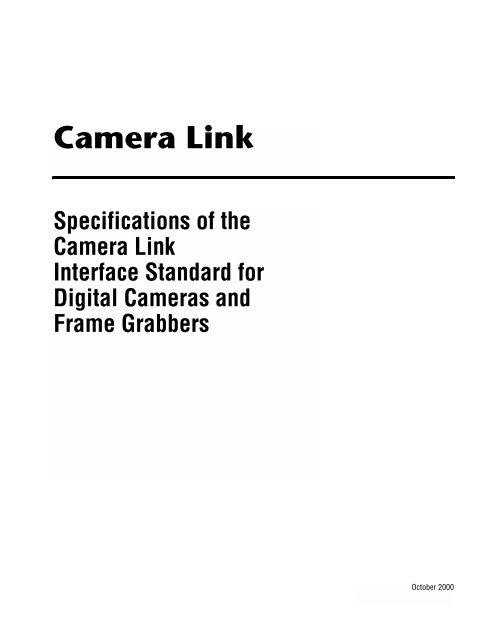
<strong>Camera</strong> <strong>Link</strong><br />
<strong>Specification</strong>s of the<br />
<strong>Camera</strong> <strong>Link</strong><br />
<strong>Interface</strong> <strong>Standard</strong> for<br />
Digital <strong>Camera</strong>s and<br />
Frame Grabbers<br />
<strong>Camera</strong> <strong>Link</strong> <strong>Specification</strong>s<br />
October 2000
Acknowledgements<br />
Participating Companies<br />
The following companies contributed to the development and definition of<br />
the <strong>Camera</strong> <strong>Link</strong> standard.<br />
• Basler<br />
• Cognex<br />
• Coreco<br />
• DALSA<br />
• Data Translation<br />
• Datacube<br />
• EPIX<br />
• Euresys<br />
• Foresight Imaging<br />
• Integral Technologies<br />
• Matrox<br />
• National Instruments<br />
• PULNiX America<br />
Rights and Trademarks<br />
PULNiX America, Inc., as chair of this ad hoc <strong>Camera</strong> <strong>Link</strong> committee, has<br />
applied for U.S. trademark protection for the term "<strong>Camera</strong> <strong>Link</strong>" to secure<br />
it for the mutual benefit of industry members. PULNiX will issue a<br />
perpetual royalty-free license to any industry member (including<br />
competitors) for the use of the "<strong>Camera</strong> <strong>Link</strong>" trademark on the condition<br />
that it is used only in conjunction with products that are fully compliant to<br />
this standard. PULNiX will not require licensed users of the trademark to<br />
credit PULNiX with ownership.<br />
3M is a trademark of the 3M Company.<br />
Channel <strong>Link</strong> is a trademark of National Semiconductor.<br />
Flatlink is a trademark of Texas Instruments.<br />
Panel <strong>Link</strong> is a trademark of Silicon <strong>Image</strong>.<br />
ii<br />
<strong>Camera</strong> <strong>Link</strong> <strong>Specification</strong>s
About this Document<br />
The following specifications provide a framework for <strong>Camera</strong> <strong>Link</strong><br />
communication. The specifications are deliberately defined to be open,<br />
allowing camera and frame grabber manufacturers to differentiate their<br />
products. Additional recommendations may be added at a later date, which<br />
will not affect the accuracy of the information in this document.<br />
iii<br />
<strong>Camera</strong> <strong>Link</strong> <strong>Specification</strong>s
Contents<br />
Acknowledgements<br />
Participating Companies ................................................................................................ii<br />
Rights and Trademarks ..................................................................................................ii<br />
About this Document<br />
Chapter 1<br />
<strong>Camera</strong> <strong>Link</strong><br />
Introduction....................................................................................................................1-1<br />
LVDS Technical Description.........................................................................................1-1<br />
Channel <strong>Link</strong>..................................................................................................................1-2<br />
Technology Benefits ......................................................................................................1-3<br />
Smaller Connectors and Cables.......................................................................1-3<br />
High Data Transmission Rates ........................................................................1-3<br />
Chapter 2<br />
<strong>Camera</strong> Signal Requirements<br />
Video Data.......................................................................................................2-1<br />
<strong>Camera</strong> Control Signals...................................................................................2-1<br />
Communication ...............................................................................................2-2<br />
Power...............................................................................................................2-2<br />
Chapter 3<br />
Port Assignments<br />
Port Definition.................................................................................................3-1<br />
Chapter 4<br />
Bit Assignments<br />
Chapter 5<br />
<strong>Camera</strong> <strong>Link</strong> Connections<br />
MDR 26-pin Connector...................................................................................5-1<br />
<strong>Camera</strong> <strong>Link</strong> Cable Pinout ..............................................................................5-2<br />
Shielding Recommendations...........................................................................5-3<br />
iv<br />
<strong>Camera</strong> <strong>Link</strong> <strong>Specification</strong>s
Contents<br />
Appendix A<br />
Chipset Criteria<br />
Appendix B<br />
API Functions<br />
Appendix C<br />
Bit Assignments According to Configuration<br />
Appendix D<br />
<strong>Camera</strong> <strong>Link</strong> Cabling Information<br />
Figures<br />
Figure 1-1. Channel <strong>Link</strong> Operation........................................................................ 1-2<br />
Figure 3-1. Data Routing for Base, Medium, and Full Configurations................... 3-2<br />
Figure 3-2. Block Diagram of Base, Medium, and Full Configuration .................. 3-3<br />
Figure 5-1. <strong>Camera</strong> <strong>Link</strong> Cable ............................................................................... 5-1<br />
Figure D-1. Dimensions of 3M Connector............................................................... D-1<br />
Figure D-2. 3M Part Number Ordering Information................................................ D-3<br />
Tables<br />
Table 3-1. Port Assignments According to Configuration..................................... 3-1<br />
Table 4-1. <strong>Camera</strong> <strong>Link</strong> Bit Assignment................................................................ 4-1<br />
Table A-1. Compatible National Semiconductor Parts........................................... A-1<br />
Table C-1. Bit Assignments for Base Configuration .............................................. C-1<br />
Table C-2. Bit Assignment for Medium Configuration.......................................... C-2<br />
Table C-3. Bit Assignment for Full Configuration ................................................. C-4<br />
Table D-1. Shell Options......................................................................................... D-3<br />
Table D-2. 3M Boardmount Receptacle Part Numbers .......................................... D-4<br />
<strong>Camera</strong> <strong>Link</strong> <strong>Specification</strong>s<br />
v
<strong>Camera</strong> <strong>Link</strong><br />
1<br />
Introduction<br />
LVDS Technical Description<br />
<strong>Camera</strong> <strong>Link</strong> is a communication interface for vision applications. The<br />
interface extends the base technology of Channel <strong>Link</strong> to provide a<br />
specification more useful for vision applications.<br />
For years, the scientific and industrial digital video market has lacked a<br />
standard method of communication. Both frame grabbers and camera<br />
manufacturers developed products with different connectors, making cable<br />
production difficult for manufacturers and very confusing for consumers. A<br />
connectivity standard between digital cameras and frame grabbers is long<br />
overdue and will become even more necessary as data rates continue to<br />
increase.<br />
Increasingly diverse cameras and advanced signal and data transmissions<br />
have made a connectivity standard like <strong>Camera</strong> <strong>Link</strong> a necessity. The<br />
<strong>Camera</strong> <strong>Link</strong> interface will reduce support time, as well as the cost of that<br />
support. The standard cable will be able to handle the increased signal<br />
speeds, and the cable assembly will allow customers to reduce their costs<br />
through volume pricing.<br />
Low Voltage Differential Signaling (LVDS) is a high-speed, low-power<br />
general purpose interface standard. The standard, known as<br />
ANSI/TIA/EIA-644, was approved in March 1996. LVDS uses differential<br />
signaling, with a nominal signal swing of 350 mV differential. The low<br />
signal swing decreases rise and fall times to achieve a theoretical maximum<br />
transmission rate of 1.923 Gbps into a loss-less medium. The low signal<br />
swing also means that the standard is not dependent on a particular supply<br />
voltage. LVDS uses current-mode drivers, which limit power consumption.<br />
The differential signals are immune to ±1 V common volt noise.<br />
1-1 <strong>Camera</strong> <strong>Link</strong> <strong>Specification</strong>s
Channel <strong>Link</strong><br />
National Semiconductor developed the Channel <strong>Link</strong> technology as a<br />
solution for flat panel displays, based on LVDS for the physical layer. The<br />
technology was then extended into a method for general purpose data<br />
transmission. Channel <strong>Link</strong> consists of a driver and receiver pair. The<br />
driver accepts 28 single-ended data signals and a single-ended clock. The<br />
data is serialized 7:1, and the four data streams and a dedicated clock are<br />
driven over five LVDS pairs. The receiver accepts the four LVDS data<br />
streams and LVDS clock, and then drives the 28 bits and a clock to the<br />
board. Figure 1-1 illustrates Channel <strong>Link</strong> operation.<br />
Driver<br />
100 Ω<br />
Receiver<br />
>1.6 Gbps<br />
Driver<br />
Data (LDVS)<br />
100Ω<br />
Receiver<br />
TTL/CMOS<br />
Data 28-bit<br />
Driver<br />
Driver<br />
Data (LDVS)<br />
Data (LDVS)<br />
Receiver<br />
Receiver<br />
TTL/CMOS<br />
Data 28-bit<br />
Driver<br />
Data (LDVS)<br />
Receiver<br />
Driver<br />
Clock (LDVS)<br />
Receiver<br />
Clock<br />
Figure 1-1. Channel <strong>Link</strong> Operation<br />
<strong>Camera</strong> <strong>Link</strong> <strong>Specification</strong>s 1-2
Technology Benefits<br />
Smaller Connectors and Cables<br />
High Data Transmission Rates<br />
Channel <strong>Link</strong>’s transmission method requires fewer conductors to transfer<br />
data. Five pairs of wires can transmit up to 28 bits of data. These wires<br />
reduce the size of the connector, allowing smaller cameras to be<br />
manufactured.<br />
The data transmission rates of the Channel <strong>Link</strong> chipset (up to 2.38 Gbits/s)<br />
support the current trend of increasing transfer speeds.<br />
1-3 <strong>Camera</strong> <strong>Link</strong> <strong>Specification</strong>s
<strong>Camera</strong> Signal Requirements<br />
2<br />
This section provides definitions for the signals used in the <strong>Camera</strong> <strong>Link</strong><br />
interface. The standard <strong>Camera</strong> <strong>Link</strong> cable provides camera control signals,<br />
serial communication, and video data.<br />
Video Data<br />
The Channel <strong>Link</strong> technology is integral to the transmission of video data.<br />
<strong>Image</strong> data and image enables are transmitted on the Channel <strong>Link</strong> bus.<br />
Four enable signals are defined as:<br />
• FVAL—Frame Valid (FVAL) is defined HIGH for valid lines.<br />
• LVAL—Line Valid (LVAL) is defined HIGH for valid pixels.<br />
• DVAL—Data Valid (DVAL) is defined HIGH when data is valid.<br />
• Spare— A spare has been defined for future use.<br />
<strong>Camera</strong> Control Signals<br />
All four enables must be provided by the camera on each Channel <strong>Link</strong><br />
chip. All unused data bits must be tied to a known value by the camera.<br />
For more information on image data bit allocations, see Section 3,<br />
Bit Assignments, and Appendix C, Bit Assignments According to<br />
Configuration.<br />
Four LVDS pairs are reserved for general-purpose camera control. They<br />
are defined as camera inputs and frame grabber outputs. <strong>Camera</strong><br />
manufacturers can define these signals to meet their needs for a particular<br />
product. The signals are:<br />
• <strong>Camera</strong> Control 1 (CC1)<br />
• <strong>Camera</strong> Control 2 (CC2)<br />
• <strong>Camera</strong> Control 3 (CC3)<br />
• <strong>Camera</strong> Control 4 (CC4)<br />
2-1 <strong>Camera</strong> <strong>Link</strong> <strong>Specification</strong>s
Communication<br />
Two LVDS pairs have been allocated for asynchronous serial<br />
communication to and from the camera and frame grabber. <strong>Camera</strong>s and<br />
frame grabbers should support at least 9600 baud. These signals are<br />
• SerTFG—Differential pair with serial communications to the frame<br />
grabber.<br />
• SerTC—Differential pair with serial communications to the camera.<br />
The serial interface will have the following characteristics: one start bit, one<br />
stop bit, no parity, and no handshaking.<br />
It is recommended that frame grabber manufacturers supply both a user<br />
interface and a software application programmming interface (API) for<br />
using the asynchronous serial communication port. The user interface will<br />
consist of a terminal program with minimal capabilities of sending and<br />
receiving a character string and sending a file of bytes. The software API<br />
will provide functions to enumerate boards and send or receive a character<br />
string. See Appendix B, API Functions, for a suggested software<br />
application program interface (API).<br />
Power<br />
Power will not be provided on the <strong>Camera</strong> <strong>Link</strong> connector. The camera will<br />
receive power through a separate cable. Each camera manufacturer will<br />
define their own power connector, current, and voltage requirements.<br />
<strong>Camera</strong> <strong>Link</strong> <strong>Specification</strong>s 2-2
Port Assignments<br />
3<br />
The <strong>Camera</strong> <strong>Link</strong> interface has three configurations. Since a single<br />
Channel <strong>Link</strong> chip is limited to 28 bits, some cameras may require several<br />
chips in order to transfer data efficiently. The naming conventions for the<br />
various configurations are:<br />
• Base—Single Channel <strong>Link</strong> chip, single cable connector.<br />
• Medium—Two Channel <strong>Link</strong> chips, two cable connectors.<br />
• Full—Three Channel <strong>Link</strong> chips, two cable connectors.<br />
Port Definition<br />
A port is defined as an 8-bit word. The Least Significant Bit (LSB) is bit 0,<br />
and the Most Significant Bit (MSB) is bit 7. The <strong>Camera</strong> <strong>Link</strong> interface<br />
utilizes the 8 ports of A-H.<br />
The following table shows the port assignment for the Base, Medium, and<br />
Full Configurations.<br />
Table 3-1. Port Assignments According to Configuration<br />
Configuration Ports Supported Number of Chips<br />
Number of<br />
Connectors<br />
Base A, B, C 1 1<br />
Medium A, B, C, D, E, F 2 2<br />
Full A, B, C, D, E, F, G, H 3 2<br />
3-1 <strong>Camera</strong> <strong>Link</strong> <strong>Specification</strong>s
<strong>Camera</strong> Hardware Routing PC Memory<br />
Port H<br />
8 bit: H0-H7 S6<br />
12 bit: D8-D11 S5<br />
BYTE 8<br />
Port G<br />
8 bit: G0-G7<br />
S4<br />
BYTE 7<br />
12 bit: D0-D7<br />
S3<br />
Port F<br />
8 bit: F0-F7<br />
12 bit: C8-C11<br />
BYTE 6<br />
Port E<br />
8 bit: E0-E7<br />
12 bit: C0-C7<br />
BYTE 5<br />
Full<br />
Port D<br />
8 bit: D0-D7<br />
S2<br />
BYTE 4<br />
Medium<br />
Port C<br />
12 bit: B8-B11<br />
8 bit: C0-C7<br />
12 bit: B0-B7<br />
S1<br />
BYTE 3<br />
Base<br />
Port B<br />
8 bit: B0-B7<br />
12 bit: A8-A11<br />
BYTE 2<br />
Port A<br />
8 bit: A0-A7<br />
12 bit: A0-A7<br />
BYTE 1<br />
Figure 3-1. Data Routing for Base, Medium, and Full Configurations<br />
The block diagram shown in Figure 3 illustrates the Base, Medium, and<br />
Full Configurations.<br />
<strong>Camera</strong> <strong>Link</strong> <strong>Specification</strong>s 3-2
<strong>Camera</strong><br />
LVAL, FVAL,<br />
DVAL, SP<br />
Port<br />
G, H<br />
STRB<br />
G, H<br />
LVAL, FVAL,<br />
DVAL, SP<br />
Port<br />
D, E, F<br />
STRB<br />
D, E, F<br />
LVAL, FVAL,<br />
DVAL, SP<br />
Port A, B, C<br />
STRB<br />
A, B, C<br />
<strong>Camera</strong><br />
Control<br />
1, 2, 3, 4<br />
TxIN<br />
90CR283<br />
TxIN<br />
90CR283<br />
TxIN<br />
90CR283<br />
Z0<br />
Z1<br />
Z2<br />
Z3<br />
CLKZ<br />
Y0<br />
Y1<br />
Y2<br />
Y3<br />
CLKY<br />
X0<br />
X1<br />
X2<br />
X3<br />
CLKX<br />
MDR26F<br />
MDR26M<br />
BASE CONFIGURATION MEDIUM FULL<br />
CONNECTOR 2<br />
CONNECTOR 1<br />
MDR26M<br />
MDR26F<br />
Z0<br />
Z1<br />
Z2<br />
Z3<br />
CLKZ<br />
Y0<br />
Y1<br />
Y2<br />
Y3<br />
CLKY<br />
X0<br />
X1<br />
X2<br />
X3<br />
CLKX<br />
90CR284<br />
90CR284<br />
90CR284<br />
Frame<br />
Grabber<br />
LVAL, FVAL,<br />
DVAL, SP<br />
PORT<br />
G, H<br />
STRB<br />
G, H<br />
LVAL, FVAL,<br />
DVAL, SP<br />
Port D, E, F<br />
STRB<br />
D, E, F<br />
LVAL, FVAL,<br />
DVAL, SP<br />
Port A, B, C<br />
STRB<br />
A, B, C<br />
<strong>Camera</strong><br />
Control<br />
1,2,3,4<br />
SerTFG<br />
SerTFG<br />
SerTC<br />
SerTC<br />
Figure 3-2. Block Diagram of Base, Medium, and Full Configuration<br />
3-3 <strong>Camera</strong> <strong>Link</strong> <strong>Specification</strong>s
Bit Assignments<br />
4<br />
The following tables list the bit allocation for the <strong>Camera</strong> <strong>Link</strong> interface.<br />
Note Ports D and G, if present, have the same device pinouts as Port A. Ports E and H, if<br />
present, have the same pinout as Port B. Port F, if present, has the same pinout as Port C.<br />
Detailed bit assignments for popular camera configurations are located in Appendix C,<br />
Bit Assignments According to Configuration.<br />
Table 4-1. <strong>Camera</strong> <strong>Link</strong> Bit Assignment<br />
Tx Input Signal Name 28-bit Solution Pin Name<br />
Strobe<br />
TxClk Out/TxClk In<br />
LVAL TX/RX 24<br />
FVAL TX/RX 25<br />
DVAL TX/RX 26<br />
Spare TX/RX 23<br />
Port A0, Port D0, Port G0 TX/RX 0<br />
Port A1, Port D1, Port G1 TX/RX 1<br />
Port A2, Port D2, Port G2 TX/RX 2<br />
Port A3, Port D3, Port G3 TX/RX 3<br />
Port A4, Port D4, Port G4 TX/RX 4<br />
Port A5, Port D5, Port G5 TX/RX 6<br />
Port A6, Port D6, Port G6 TX/RX 27<br />
Port A7, Port D7, Port G7 TX/RX 5<br />
Port B0, Port E0, Port H0 TX/RX 7<br />
Port B1, Port E1, Port H1 TX/RX 8<br />
Port B2, Port E2, Port H2 TX/RX 9<br />
4-1 <strong>Camera</strong> <strong>Link</strong> <strong>Specification</strong>s
Table 4-1. <strong>Camera</strong> <strong>Link</strong> Bit Assignment (Continued)<br />
Tx Input Signal Name 28-bit Solution Pin Name<br />
Port B3, Port E3, Port H3 TX/RX 12<br />
Port B4, Port E4, Port H4 TX/RX 13<br />
Port B5, Port E5, Port H5 TX/RX 14<br />
Port B6, Port E6, Port H6 TX/RX 10<br />
Port B7, Port E7, Port H7 TX/RX 11<br />
Port C0, Port F0 TX/RX 15<br />
Port C1, Port F1 TX/RX 18<br />
Port C2, Port F2 TX/RX 19<br />
Port C3, Port F3 TX/RX 20<br />
Port C4, Port F4 TX/RX 21<br />
Port C5, Port F5 TX/RX 22<br />
Port C6, Port F6 TX/RX 16<br />
Port C7, Port F7 TX/RX 17<br />
<strong>Camera</strong> <strong>Link</strong> <strong>Specification</strong>s 4-2
<strong>Camera</strong> <strong>Link</strong> Connections<br />
5<br />
MDR 26-pin Connector<br />
The MDR 26-pin connector was selected for its robust design and<br />
reputation for success with the high-frequency transfer rates of Channel<br />
<strong>Link</strong>. During the past four years, 3M has worked very closely with National<br />
Semiconductor to test and define the performance of the high-speed MDR<br />
connector for use with the LVDS transmissions.<br />
26-Position<br />
High-Density<br />
Mini D Ribbon<br />
(MDR) Male Plug<br />
Cable<br />
(See pinout for cable construction)<br />
26-Position<br />
High-Density<br />
Mini D Ribbon<br />
(MDR) Male Plug<br />
2X<br />
Thumbscrews<br />
2X<br />
Thumbscrews<br />
Figure 5-1. <strong>Camera</strong> <strong>Link</strong> Cable<br />
5-1 <strong>Camera</strong> <strong>Link</strong> <strong>Specification</strong>s
<strong>Camera</strong> <strong>Link</strong> Cable Pinout<br />
Medium and Full Configurations<br />
<strong>Camera</strong><br />
Connector<br />
Frame<br />
Grabber<br />
Connector<br />
Table 5-1. MDR-26 Connector Assignments<br />
Channel<br />
<strong>Link</strong><br />
Signal<br />
1 1 inner<br />
shield<br />
14 14 inner<br />
shield<br />
Cable<br />
Name<br />
Inner<br />
Shield<br />
Inner<br />
Shield<br />
.<br />
Base Configuration (with <strong>Camera</strong><br />
Control and Serial Communication)<br />
<strong>Camera</strong><br />
Connector<br />
Frame<br />
Grabber<br />
Connector<br />
Channel<br />
<strong>Link</strong><br />
Signal<br />
1 1 inner<br />
shield<br />
14 14 inner<br />
shield<br />
2 25 Y0- PAIR1- 2 25 X0-<br />
15 12 Y0+ PAIR1+ 15 12 X0+<br />
3 24 Y1- PAIR2- 3 24 X1-<br />
16 11 Y1+ PAIR2+ 16 11 X1+<br />
4 23 Y2- PAIR3- 4 23 X2-<br />
17 10 Y2+ PAIR3+ 17 10 X2+<br />
5 22 Yclk- PAIR4- 5 22 Xclk-<br />
18 9 Yclk+ PAIR4+ 18 9 Xclk+<br />
6 21 Y3- PAIR5- 6 21 X3-<br />
19 8 Y3+ PAIR5+ 19 8 X3+<br />
7 20 100 Ω PAIR6+ 7 20 SerTC+<br />
20 7 terminated PAIR6- 20 7 SerTC-<br />
8 19 Z0- PAIR7- 8 19 SerTFG-<br />
21 6 Z0+ PAIR7+ 21 6 SerTFG+<br />
9 18 Z1- PAIR8- 9 18 CC1-<br />
22 5 Z1+ PAIR8+ 22 5 CC1+<br />
10 17 Z2- PAIR9+ 10 17 CC2+<br />
23 4 Z2+ PAIR9- 23 4 CC2-<br />
<strong>Camera</strong> <strong>Link</strong> <strong>Specification</strong>s 5-2
Medium and Full Configurations<br />
<strong>Camera</strong><br />
Connector<br />
Frame<br />
Grabber<br />
Connector<br />
23 4 Z2+ PAIR9- 23 4 CC2-<br />
11 16 Zclk- PAIR10- 11 16 CC3-<br />
24 3 Zclk+ PAIR10+ 24 3 CC3+<br />
12 15 Z3- PAIR11+ 12 15 CC4+<br />
25 2 Z3+ PAIR11- 25 2 CC4-<br />
13 13 inner<br />
shield<br />
26 26 inner<br />
shield<br />
Shielding Recommendations<br />
Table 5-1. MDR-26 Connector Assignments (Continued)<br />
Channel<br />
<strong>Link</strong><br />
Signal<br />
Cable<br />
Name<br />
Inner<br />
Shield<br />
Inner<br />
Shield<br />
Base Configuration (with <strong>Camera</strong><br />
Control and Serial Communication)<br />
<strong>Camera</strong><br />
Connector<br />
Frame<br />
Grabber<br />
Connector<br />
Channel<br />
<strong>Link</strong><br />
Signal<br />
13 13 inner<br />
shield<br />
26 26 inner<br />
shield<br />
The outer shield of the cable is tied to the connector shell. It is<br />
recommended that the inner shell be tied to digital ground in cameras and<br />
tied through a resister to digital ground in the frame grabbers. It is<br />
recommended that a 0 Ω resistor be installed in the factory. If necessary,<br />
that resistor can be removed in the field and replaced with a high-value<br />
resistor and parallel capacitor. Unused pairs should be terminated to 100 Ω<br />
at their respective ends of the cable.<br />
Note All pairs are individually shielded with aluminum foil. Pair shields are wrapped<br />
aluminum out and are in contact with four internal drains (digital ground). Outer braid and<br />
foil (chassis ground) are isolated from inner drains (digital ground).<br />
5-3 <strong>Camera</strong> <strong>Link</strong> <strong>Specification</strong>s
Chipset Criteria<br />
A<br />
<strong>Camera</strong> <strong>Link</strong> uses 28-bit Channel <strong>Link</strong> chips manufactured by National<br />
Semiconductor. Because of potential interface issues, chips that use a<br />
similar technology, such as Flatlink by Texas Instruments and Panel <strong>Link</strong><br />
by Silicon <strong>Image</strong>, may not be compatible with the <strong>Camera</strong> <strong>Link</strong> interface.<br />
Receivers and drivers with different operating frequencies will interoperate<br />
over the frequency range that both support. The following table lists some<br />
compatible National Semiconductor parts.<br />
Table A-1. Compatible National Semiconductor Parts<br />
Product Supply Voltage Speed<br />
DS90CR281 5 V 40 MHz<br />
DS90CR282 5 V 40 MHz<br />
DS90CR283 5 V 66 MHz<br />
DS90CR284 5 V 66 MHz<br />
DS90CR285 3.3 V 66 MHz<br />
DS90CR286 3.3 V 66 MHz<br />
DS90CR286A 3.3 V 66 MHz<br />
DS90CR287 3.3 V 85 MHz<br />
DS90CR288 3.3 V 75 MHz<br />
DS90CR288A 3.3 V 85 MHz<br />
The pinout of the MDR 26 connector was chosen for optimal PWB trace<br />
routing using an LVDS driver/receiver pair for camera control signals. The<br />
following are the recommended National Semiconductor parts for the pair:<br />
DS90LV047 3.3 V transmitter<br />
DS90LV048 3.3 V receiver<br />
A-1 <strong>Camera</strong> <strong>Link</strong> <strong>Specification</strong>s
API Functions<br />
B<br />
A consistent, known API for asynchronous serial reading and writing<br />
allows camera vendors to write a frame grabber-independent,<br />
camera-specific configuration utility. The following API offers a solution<br />
for camera vendors that is easy for frame grabber manufacturers to<br />
implement, regardless of the actual implementation methods used for<br />
asynchronous serial communication.<br />
All frame grabbers provide a .dll file named clser***.dll, where ***<br />
is specific to the frame grabber vendor. There are four functions within<br />
that .dll:<br />
• clSerialInit—Initialize the serial communication for<br />
a specific board.<br />
• clSerialRead—Read bytes from the camera.<br />
• clSerialWrite—Write bytes to the camera.<br />
• clSerialClose—Close the serial communication.<br />
B-1 <strong>Camera</strong> <strong>Link</strong> <strong>Specification</strong>s
clSerialInit<br />
Format<br />
int clSerialInit(unsigned long serialIndex, void** serialRefPtr)<br />
Purpose<br />
This function initializes the device referred to by serialIndex, and returns a pointer to an<br />
internal serial reference structure.<br />
Parameters<br />
Name Direction Description<br />
serialIndex input A zero-based index value. For n<br />
serial devices in the system<br />
supported by this library,<br />
serialIndex has a range of<br />
0to(n-1).<br />
serialRefPtr output Points to a value that contains, on a<br />
successful call, a pointer to the<br />
vendor-specific reference to the<br />
current session.<br />
Return Value<br />
A vendor-specific error value that follows these conventions:<br />
• A negative value indicates a fatal error.<br />
• A zero value indicates success.<br />
• A positive value indicates a warning.<br />
<strong>Camera</strong> <strong>Link</strong> <strong>Specification</strong>s B-2
clSerialRead<br />
Format<br />
int clSerialRead(void* serialRef, char* buffer,unsigned long* bufferSize<br />
unsigned long serialTimeout)<br />
Purpose<br />
This function reads the serial device referenced by serialRef.<br />
Parameters<br />
Name Direction Description<br />
serialRef input The value obtained from the<br />
clSerialInit function.<br />
buffer output Points to a user-allocated buffer.<br />
Upon a successful call, buffer<br />
contains the data read from the<br />
serial device.<br />
bufferSize input/output Contains the buffer size indicating<br />
the maximum number of bytes that<br />
the buffer can accommodate. Upon<br />
a successful call, bufferSize<br />
contains the number of bytes read<br />
successfully from the serial device.<br />
serialTimeout input Indicates the timeout in<br />
milliseconds.<br />
Return Value<br />
A vendor-specific error value that follows these conventions:<br />
• A negative value indicates a fatal error.<br />
• A zero value indicates success.<br />
• A positive value indicates a warning.<br />
B-3 <strong>Camera</strong> <strong>Link</strong> <strong>Specification</strong>s
clSerialWrite<br />
Format<br />
int clSerialWrite(void* serialRef, char* buffer,unsigned long* bufferSize<br />
unsigned long SerialTimeout)<br />
Purpose<br />
This function writes the data in the buffer to the serial device referenced by SerialRef.<br />
Parameters<br />
Name Direction Description<br />
serialRef input The value obtained from the<br />
clSerialInit function.<br />
buffer input Contains data to write to the serial<br />
port.<br />
bufferSize input/output Contains the buffer size indicating<br />
the maximum number of bytes that<br />
the buffer can accommodate. Upon<br />
a successful call, bufferSize<br />
contains the number of bytes read<br />
successfully from the serial device.<br />
serialTimeout input Indicates the timeout in<br />
milliseconds.<br />
Return Value<br />
A vendor-specific error value that follows these conventions:<br />
• A negative value indicates a fatal error.<br />
• A zero value indicates success.<br />
• A positive value indicates a warning.<br />
<strong>Camera</strong> <strong>Link</strong> <strong>Specification</strong>s B-4
clSerialClose<br />
Format<br />
void clSerialClose(void* serialRef)<br />
Purpose<br />
This function closes the serial device and cleans up the resources associated with serialRef.<br />
Upon return, serialRef is no longer usable.<br />
Parameters<br />
Name Direction Description<br />
serialRef input The value obtained from the<br />
clSerialInit function for<br />
clean up.<br />
Return Value<br />
A vendor-specific error value that follows these conventions:<br />
• A negative value indicates a fatal error.<br />
• A zero value indicates success.<br />
• A positive value indicates a warning.<br />
B-5 <strong>Camera</strong> <strong>Link</strong> <strong>Specification</strong>s
Header File<br />
The following is an example of an appropriate header file for this API:<br />
#ifndef _CLSER____H_<br />
#define _CLSER____H_<br />
#ifndef CLSER___EXPORT<br />
#define CLSER___EXPORT __declspec(dllimport)<br />
#endif<br />
#ifndef CLSER___CC<br />
#define CLSER___CC __cdecl<br />
#endif<br />
#ifdef __cplusplus<br />
extern "C"{<br />
#endif<br />
CLSER___EXPORT int CLSER___CC<br />
clSerialInit(unsigned long serialIndex, void** serialRefPtr);<br />
CLSER___EXPORT int CLSER___CC<br />
clSerialRead(void* serialRef, char* buffer,unsigned long* bufferSize,<br />
unsigned long serialTimeout);<br />
CLSER___EXPORT int CLSER___CC<br />
clSerialWrite(void* serialRef, char* buffer, unsigned long* bufferSize,<br />
unsigned long serialTimeout);<br />
CLSER___EXPORT void CLSER___CC<br />
clSerialClose(void* serialRef);<br />
#ifdef __cplusplus<br />
}<br />
#endif<br />
#endif<br />
<strong>Camera</strong> <strong>Link</strong> <strong>Specification</strong>s B-6
Note Using a single .dll file prevents the user from accessing driver software from<br />
multiple vendors at the same time; therefore, camera vendors using this API must load all<br />
.dll files with the name clser*.dll on the system and then provide a method for the<br />
user to select the correct vendor for the board they are using. The camera vendor should<br />
use LoadLibrary and GetProcAddress to find these functions. The camera vendors<br />
should also provide a way for users to select a particular frame grabber, and then use<br />
clSerialRead and clSerialWrite to communicate with the camera attached to<br />
their board.<br />
B-7 <strong>Camera</strong> <strong>Link</strong> <strong>Specification</strong>s
Bit Assignments According to<br />
Configuration<br />
C<br />
Port/bit<br />
8-bit x<br />
1~3*<br />
Table C-1. Bit Assignments for Base Configuration<br />
10-bit x<br />
1~2<br />
Base Configuration<br />
12-bit x<br />
1~2 14-bit x 1 16-bit x 1<br />
Port A0 A0 A0 A0 A0 A0 R0<br />
Port A1 A1 A1 A1 A1 A1 R1<br />
Port A2 A2 A2 A2 A2 A2 R2<br />
Port A3 A3 A3 A3 A3 A3 R3<br />
Port A4 A4 A4 A4 A4 A4 R4<br />
Port A5 A5 A5 A5 A5 A5 R5<br />
Port A6 A6 A6 A6 A6 A6 R6<br />
Port A7 A7 A7 A7 A7 A7 R7<br />
24-bit<br />
RGB<br />
Port B0 B0 A8 A8 A8 A8 G0<br />
Port B1 B1 A9 A9 A9 A9 G1<br />
Port B2 B2 nc A10 A10 A10 G2<br />
Port B3 B3 nc A11 A11 A11 G3<br />
Port B4 B4 B8 B8 A12 A12 G4<br />
Port B5 B5 B9 B9 A13 A13 G5<br />
Port B6 B6 nc B10 nc A14 G6<br />
Port B7 B7 nc B11 nc A15 G7<br />
Port C0 C0 B0 B0 nc nc B0<br />
Port C1 C1 B1 B1 nc nc B1<br />
C-1 <strong>Camera</strong> <strong>Link</strong> <strong>Specification</strong>s
Port/bit<br />
8-bit x<br />
1~3*<br />
Table C-1. Bit Assignments for Base Configuration (Continued)<br />
10-bit x<br />
1~2<br />
Base Configuration<br />
12-bit x<br />
1~2 14-bit x 1 16-bit x 1<br />
Port C2 C2 B2 B2 nc nc B2<br />
Port C3 C3 B3 B3 nc nc B3<br />
Port C4 C4 B4 B4 nc nc B4<br />
Port C5 C5 B5 B5 nc nc B5<br />
Port C6 C6 B6 B6 nc nc B6<br />
Port C7 C7 B7 B7 nc nc B7<br />
* If only using a single channel, use Port A. If using two channels, use Port A and B.<br />
24-bit<br />
RGB<br />
Table C-2. Bit Assignment for Medium Configuration<br />
Medium Configuration<br />
Port/bit 8-bit x 4 10-bit x 3~4 12-bit x 3~4 30-bit RGB 36-bit RGB<br />
Port A0 A0 A0 A0 R0 R0<br />
Port A1 A1 A1 A1 R1 R1<br />
Port A2 A2 A2 A2 R2 R2<br />
Port A3 A3 A3 A3 R3 R3<br />
Port A4 A4 A4 A4 R4 R4<br />
Port A5 A5 A5 A5 R5 R5<br />
Port A6 A6 A6 A6 R6 R6<br />
Port A7 A7 A7 A7 R7 R7<br />
Port B0 B0 A8 A8 R8 R8<br />
Port B1 B1 A9 A9 R9 R9<br />
Port B2 B2 nc A10 nc R10<br />
Port B3 B3 nc A11 nc R11<br />
Port B4 B4 B8 B8 B8 B8<br />
<strong>Camera</strong> <strong>Link</strong> <strong>Specification</strong>s C-2
Table C-2. Bit Assignment for Medium Configuration (Continued)<br />
Medium Configuration<br />
Port/bit 8-bit x 4 10-bit x 3~4 12-bit x 3~4 30-bit RGB 36-bit RGB<br />
Port B5 B5 B9 B9 B9 B9<br />
Port B6 B6 nc B10 nc B10<br />
Port B7 B7 nc B11 nc B11<br />
Port C0 C0 B0 B0 B0 B0<br />
Port C1 C1 B1 B1 B1 B1<br />
Port C2 C2 B2 B2 B2 B2<br />
Port C3 C3 B3 B3 B3 B3<br />
Port C4 C4 B4 B4 B4 B4<br />
Port C5 C5 B5 B5 B5 B5<br />
Port C6 C6 B6 B6 B6 B6<br />
Port C7 C7 B7 B7 B7 B7<br />
Port D0 D0 D0 D0 nc nc<br />
Port D1 D1 D1 D1 nc nc<br />
Port D2 D2 D2 D2 nc nc<br />
Port D3 D3 D3 D3 nc nc<br />
Port D4 D4 D4 D4 nc nc<br />
Port D5 D5 D5 D5 nc nc<br />
Port D6 D6 D6 D6 nc nc<br />
Port D7 D7 D7 D7 nc nc<br />
Port E0 nc C0 C0 G0 G0<br />
Port E1 nc C1 C1 G1 G1<br />
Port E2 nc C2 C2 G2 G2<br />
Port E3 nc C3 C3 G3 G3<br />
Port E4 nc C4 C4 G4 G4<br />
Port E5 nc C5 C5 G5 G5<br />
C-3 <strong>Camera</strong> <strong>Link</strong> <strong>Specification</strong>s
Table C-2. Bit Assignment for Medium Configuration (Continued)<br />
Medium Configuration<br />
Port/bit 8-bit x 4 10-bit x 3~4 12-bit x 3~4 30-bit RGB 36-bit RGB<br />
Port E6 nc C6 C6 G6 G6<br />
Port E7 nc C7 C7 G7 G7<br />
Port F0 nc C8 C8 G8 G8<br />
Port F1 nc C9 C9 G9 G9<br />
Port F2 nc nc C10 nc G10<br />
Port F3 nc nc C11 nc G11<br />
Port F4 nc D8 D8 nc nc<br />
Port F5 nc D9 D9 nc nc<br />
Port F6 nc nc D10 nc nc<br />
Port F7 nc nc D11 nc nc<br />
Table C-3. Bit Assignment for Full Configuration<br />
Full Configuration<br />
Port/bit 8-bit x 8 Port/bit 8-bit x 8<br />
Port A0 A0 Port E0 E0<br />
Port A1 A1 Port E1 E1<br />
Port A2 A2 Port E2 E2<br />
Port A3 A3 Port E3 E3<br />
Port A4 A4 Port E4 E4<br />
Port A5 A5 Port E5 E5<br />
Port A6 A6 Port E6 E6<br />
Port A7 A7 Port E7 E7<br />
Port B0 B0 Port F0 F0<br />
Port B1 B1 Port F1 F1<br />
Port B2 B2 Port F2 F2<br />
<strong>Camera</strong> <strong>Link</strong> <strong>Specification</strong>s C-4
Table C-3. Bit Assignment for Full Configuration (Continued)<br />
Full Configuration<br />
Port/bit 8-bit x 8 Port/bit 8-bit x 8<br />
Port B3 B3 Port F3 F3<br />
Port B4 B4 Port F4 F4<br />
Port B5 B5 Port F5 F5<br />
Port B6 B6 Port F6 F6<br />
Port B7 B7 Port F7 F7<br />
Port C0 C0 Port G0 G0<br />
Port C1 C1 Port G1 G1<br />
Port C2 C2 Port G2 G2<br />
Port C3 C3 Port G3 G3<br />
Port C4 C4 Port G4 G4<br />
Port C5 C5 Port G5 G5<br />
Port C6 C6 Port G6 G6<br />
Port C7 C7 Port G7 G7<br />
Port D0 D0 Port H0 H0<br />
Port D1 D1 Port H1 H1<br />
Port D2 D2 Port H2 H2<br />
Port D3 D3 Port H3 H3<br />
Port D4 D4 Port H4 H4<br />
Port D5 D5 Port H5 H5<br />
Port D6 D6 Port H6 H6<br />
Port D7 D7 Port H7 H7<br />
C-5 <strong>Camera</strong> <strong>Link</strong> <strong>Specification</strong>s
<strong>Camera</strong> <strong>Link</strong> Cabling<br />
Information<br />
D<br />
The <strong>Camera</strong> <strong>Link</strong> interface uses a cable assembly manufactured by 3M,<br />
with MDR-26 pin connectors on both ends, as shown in Figure D-1.<br />
.<br />
B<br />
1 3 5 7 8<br />
2 4 6 9<br />
15 17 19<br />
22<br />
14 16 18 20 21<br />
10<br />
23<br />
11 12 13<br />
24 25 26<br />
C<br />
Generic End Detail<br />
MDR 26 Position Plug<br />
(Both Ends)<br />
Note: Use 3M 3341-31 jacksocket for mounting receptacle to panel.<br />
Cable <strong>Specification</strong>s<br />
Figure D-1. Dimensions of the 3M Connector<br />
3M’s twin-axial shielded cable has been specifically designed to meet the<br />
stringent demands of reliable high-speed differential signaling<br />
applications.<br />
Cable Assembly<br />
The <strong>Camera</strong> <strong>Link</strong> cable assembly is available in two shell configurations,<br />
and various lengths. Table D-1 describes the specifications for the<br />
following options:<br />
• Thumbscrew overmold shell—The inner IDC assembly is wrapped<br />
with a copper foil tape, which connects the outer chassis cable ground<br />
to the face of the MDR plug. A final overmolded shell is made from<br />
PVC material.<br />
• Thumbscrew shell kit—An inner metal shroud connects the chassis<br />
ground from the cable to the face of the MDR plug. A plastic “shell<br />
boot” is slipped over the metal shrouds, providing the finished shell.<br />
D-1 <strong>Camera</strong> <strong>Link</strong> <strong>Specification</strong>s
Table D-1. Shell Options<br />
Shell Option B C<br />
Thumbscrew<br />
Overmold Shell<br />
Thumbscrew<br />
Shell Kit<br />
Ordering Information<br />
1.58<br />
[40.2]<br />
1.55<br />
[39.4]<br />
.55<br />
[14.0]<br />
.51<br />
[12.8]<br />
Cable Assembly Part Numbers<br />
Cable assemblies and boardmount receptacles are available from 3M. For<br />
more information on 3M products, see the 3M Web site at www.3M.com.<br />
14X26-SZLB-XXX-0LC<br />
Shell Retention Options:<br />
B = Thumbscrew shell kit<br />
T = Thumbscrew overmold shell<br />
Length<br />
100 = 1 meter<br />
200 = 2 meters<br />
300 = 3 meters<br />
450 = 4.5 meters<br />
500 = 5 meters<br />
700 = 7 meters<br />
A00 = 10 meters<br />
Figure D-2. 3M Part Number Ordering Information<br />
<strong>Camera</strong> <strong>Link</strong> <strong>Specification</strong>s D-2
Boardmount Receptacle Part Numbers<br />
The following table lists the 3M boardmount receptacle part numbers.<br />
Table D-2. 3M Boardmount Receptacle Part Numbers<br />
Part Number Type Mount<br />
N10226-52xxVC MDR 26 Right Angle Thru-hole<br />
10266-55G3VC MDR 26 Right Angle Thru-hole<br />
10226-6212VC MDR 26 Vertical Thru-hole<br />
10226-1A10VE MDR 26 Right Angle SMT<br />
10226-2200VE MDR 26 Vertical SMT<br />
D-3 <strong>Camera</strong> <strong>Link</strong> <strong>Specification</strong>s