A robust feedforward compensation scheme for multistage ...
A robust feedforward compensation scheme for multistage ...
A robust feedforward compensation scheme for multistage ...

You also want an ePaper? Increase the reach of your titles
YUMPU automatically turns print PDFs into web optimized ePapers that Google loves.
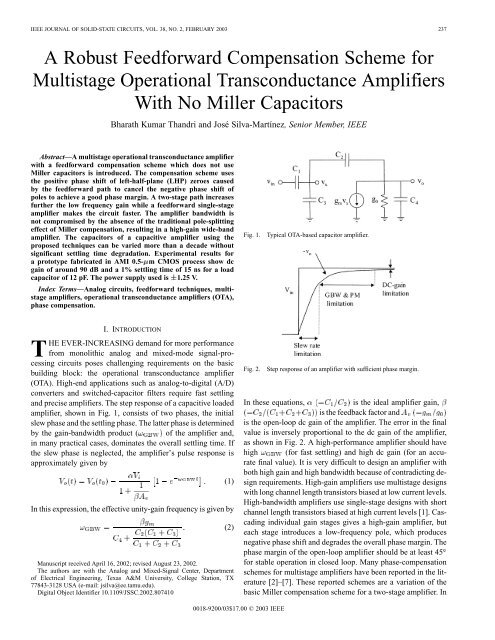
IEEE JOURNAL OF SOLID-STATE CIRCUITS, VOL. 38, NO. 2, FEBRUARY 2003 237<br />
A Robust Feed<strong>for</strong>ward Compensation Scheme <strong>for</strong><br />
Multistage Operational Transconductance Amplifiers<br />
With No Miller Capacitors<br />
Bharath Kumar Thandri and José Silva-Martínez, Senior Member, IEEE<br />
Abstract—A <strong>multistage</strong> operational transconductance amplifier<br />
with a <strong>feed<strong>for</strong>ward</strong> <strong>compensation</strong> <strong>scheme</strong> which does not use<br />
Miller capacitors is introduced. The <strong>compensation</strong> <strong>scheme</strong> uses<br />
the positive phase shift of left-half-plane (LHP) zeroes caused<br />
by the <strong>feed<strong>for</strong>ward</strong> path to cancel the negative phase shift of<br />
poles to achieve a good phase margin. A two-stage path increases<br />
further the low frequency gain while a <strong>feed<strong>for</strong>ward</strong> single-stage<br />
amplifier makes the circuit faster. The amplifier bandwidth is<br />
not compromised by the absence of the traditional pole-splitting<br />
effect of Miller <strong>compensation</strong>, resulting in a high-gain wide-band<br />
amplifier. The capacitors of a capacitive amplifier using the<br />
proposed techniques can be varied more than a decade without<br />
significant settling time degradation. Experimental results <strong>for</strong><br />
a prototype fabricated in AMI 0.5- m CMOS process show dc<br />
gain of around 90 dB and a 1% settling time of 15 ns <strong>for</strong> a load<br />
capacitor of 12 pF. The power supply used is 1.25 V.<br />
Index Terms—Analog circuits, <strong>feed<strong>for</strong>ward</strong> techniques, <strong>multistage</strong><br />
amplifiers, operational transconductance amplifiers (OTA),<br />
phase <strong>compensation</strong>.<br />
Fig. 1.<br />
Typical OTA-based capacitor amplifier.<br />
I. INTRODUCTION<br />
THE EVER-INCREASING demand <strong>for</strong> more per<strong>for</strong>mance<br />
from monolithic analog and mixed-mode signal-processing<br />
circuits poses challenging requirements on the basic<br />
building block: the operational transconductance amplifier<br />
(OTA). High-end applications such as analog-to-digital (A/D)<br />
converters and switched-capacitor filters require fast settling<br />
and precise amplifiers. The step response of a capacitive loaded<br />
amplifier, shown in Fig. 1, consists of two phases, the initial<br />
slew phase and the settling phase. The latter phase is determined<br />
by the gain-bandwidth product ( of the amplifier and,<br />
in many practical cases, dominates the overall settling time. If<br />
the slew phase is neglected, the amplifier’s pulse response is<br />
approximately given by<br />
In this expression, the effective unity-gain frequency is given by<br />
Manuscript received April 16, 2002; revised August 23, 2002.<br />
The authors are with the Analog and Mixed-Signal Center, Department<br />
of Electrical Engineering, Texas A&M University, College Station, TX<br />
77843-3128 USA (e-mail: jsilva@ee.tamu.edu).<br />
Digital Object Identifier 10.1109/JSSC.2002.807410<br />
(1)<br />
(2)<br />
Fig. 2.<br />
Step response of an amplifier with sufficient phase margin.<br />
In these equations,<br />
is the ideal amplifier gain,<br />
is the feedback factor and<br />
is the open-loop dc gain of the amplifier. The error in the final<br />
value is inversely proportional to the dc gain of the amplifier,<br />
as shown in Fig. 2. A high-per<strong>for</strong>mance amplifier should have<br />
high (<strong>for</strong> fast settling) and high dc gain (<strong>for</strong> an accurate<br />
final value). It is very difficult to design an amplifier with<br />
both high gain and high bandwidth because of contradicting design<br />
requirements. High-gain amplifiers use <strong>multistage</strong> designs<br />
with long channel length transistors biased at low current levels.<br />
High-bandwidth amplifiers use single-stage designs with short<br />
channel length transistors biased at high current levels [1]. Cascading<br />
individual gain stages gives a high-gain amplifier, but<br />
each stage introduces a low-frequency pole, which produces<br />
negative phase shift and degrades the overall phase margin. The<br />
phase margin of the open-loop amplifier should be at least 45<br />
<strong>for</strong> stable operation in closed loop. Many phase-<strong>compensation</strong><br />
<strong>scheme</strong>s <strong>for</strong> <strong>multistage</strong> amplifiers have been reported in the literature<br />
[2]–[7]. These reported <strong>scheme</strong>s are a variation of the<br />
basic Miller <strong>compensation</strong> <strong>scheme</strong> <strong>for</strong> a two-stage amplifier. In<br />
0018-9200/03$17.00 © 2003 IEEE
238 IEEE JOURNAL OF SOLID-STATE CIRCUITS, VOL. 38, NO. 2, FEBRUARY 2003<br />
Fig. 3.<br />
Block diagram of basic NCFF <strong>compensation</strong> <strong>scheme</strong> <strong>for</strong> two-stage amplifier.<br />
a Miller compensated amplifier, the dominant pole is pushed to<br />
lower frequencies due to the Miller effect (pole splitting), resulting<br />
in lower bandwidth structures. Also, a right-half-plane<br />
(RHP) zero is created which degrades the phase response. A<br />
nulling resistor is usually used to cancel the effect of the RHP<br />
zero. Other reported <strong>scheme</strong>s use the positive phase shift of a<br />
left-half-plane (LHP) zero created by a <strong>feed<strong>for</strong>ward</strong> path to improve<br />
the phase response [2], [4], but all of these still use Miller<br />
capacitors. Recently, active <strong>feed<strong>for</strong>ward</strong> techniques have been<br />
used <strong>for</strong> the design of <strong>multistage</strong> amplifiers. In [11], a theoretical<br />
analysis on the effects of <strong>feed<strong>for</strong>ward</strong> networks is presented, and<br />
in [12], the technique is used <strong>for</strong> the design of low-frequency instrumentation<br />
amplifiers.<br />
The <strong>compensation</strong> <strong>scheme</strong> used in this paper employs a <strong>feed<strong>for</strong>ward</strong><br />
path to create LHP zeros, but does not use any Miller<br />
capacitor. The dominant pole is not pushed to lower frequencies,<br />
resulting in a higher gain-bandwidth product with a fast<br />
step response. The proposed <strong>compensation</strong> <strong>scheme</strong> is described<br />
in Section II. The effects of pole–zero mismatch on the per<strong>for</strong>mance<br />
of the amplifier are discussed in Section III. It is shown<br />
that the proposed technique is <strong>robust</strong> even if the integrating and<br />
load capacitors are varied by more than a decade. Section IV<br />
describes the circuit implementation. The simulation and experimental<br />
results are discussed in Section V, and conclusions are<br />
drawn in Section VI.<br />
(a)<br />
(b)<br />
Fig. 4. Amplifier frequency response and pole–zero locations in open and<br />
closed loop. (a) Perfect pole–zero cancellation. (b) Pole–zero mismatch.<br />
II. NO-CAPACITOR FEEDFORWARD (NCFF) COMPENSATION<br />
SCHEME FOR MULTISTAGE AMPLIFIERS<br />
stages have a common pole at<br />
amplifier voltage gain is<br />
. The overall<br />
The proposed NCFF <strong>compensation</strong> <strong>scheme</strong> alleviates the<br />
drawbacks of Miller <strong>compensation</strong> <strong>scheme</strong>s. The block diagram<br />
of the NCFF <strong>scheme</strong> is shown in Fig. 3. The <strong>compensation</strong><br />
<strong>scheme</strong> uses the positive phase shift of LHP zeros, created by<br />
a <strong>feed<strong>for</strong>ward</strong> path, to compensate the negative phase shift due<br />
to the poles. The pole–zero pair is created at high frequencies<br />
to avoid slow settling components associated with pole–zero<br />
cancellation at low frequencies [8]. The main concept can be<br />
explained by assuming a single-pole response <strong>for</strong> the three<br />
blocks. , , and are the dc gains of the first, second,<br />
and <strong>feed<strong>for</strong>ward</strong> stages of the amplifier. The pole of the first<br />
stage is located at<br />
and the second and third<br />
The OTA transfer function has two poles and a LHP zero created<br />
by the <strong>feed<strong>for</strong>ward</strong> path. The dc gain is given by<br />
(3)
THANDRI AND SILVA-MARTÍNEZ: ROBUST FEEDFORWARD COMPENSATION SCHEME FOR MULTISTAGE OTAS WITH NO MILLER CAPACITORS 239<br />
Fig. 5.<br />
NCFF <strong>compensation</strong> <strong>scheme</strong> <strong>for</strong> n-stage amplifier.<br />
and the dominant pole is located at<br />
zero is<br />
. The location of the LHP<br />
Notice that the location of the LHP zero is approximately at<br />
times the gain-bandwidth product of the first stage, where<br />
. The second and <strong>feed<strong>for</strong>ward</strong> stages can be designed<br />
such that the negative phase shift due to is compensated by<br />
the positive phase shift of the LHP zero. When the frequency of<br />
exactly coincides with that of the LHP zero, the amplifier<br />
phase margin is 90 and the unity-gain frequency is given by<br />
. The open- and closed-loop transfer<br />
functions <strong>for</strong> perfect and imperfect pole–zero cancellation are<br />
shown in Fig. 4(a) and (b), respectively. The implications of<br />
pole–zero mismatch are discussed in Section III.<br />
This <strong>compensation</strong> <strong>scheme</strong> results in an amplifier with high<br />
gain and fast response. The bandwidth improvement is due to<br />
the fact that the poles are not split, as is the case in any amplifier<br />
with Miller <strong>compensation</strong>. There can be a substantial reduction<br />
in area and power, especially as compared to <strong>multistage</strong><br />
amplifiers, which use two or more capacitors <strong>for</strong> phase <strong>compensation</strong>.<br />
If the nondominant pole of the first stage is also considered,<br />
then the resulting transfer function has three poles and two<br />
LHP zeros. In general, the number of LHP zeros created by the<br />
<strong>feed<strong>for</strong>ward</strong> path is equal to the order of the first stage. The main<br />
restriction here is that the nondominant pole of the <strong>feed<strong>for</strong>ward</strong><br />
and second stage must be placed after the overall unity-gain<br />
bandwidth of the amplifier in order to minimize phase degradation.<br />
This <strong>compensation</strong> <strong>scheme</strong> can be extended <strong>for</strong> a generic<br />
-stage amplifier, as shown in Fig. 5.<br />
III. OPTIMIZATION OF CLOSED-LOOP RESPONSE<br />
The OTA is commonly used in closed-loop configuration with<br />
feedback capacitors as shown in Fig. 1. Imperfect pole–zero<br />
cancellation results in a pole–zero doublet that might affect the<br />
(4)<br />
per<strong>for</strong>mance of the amplifier. The transconductances of individual<br />
gain stages should be selected properly to alleviate this<br />
drawback, as shown in the following discussion.<br />
It has already been shown that a pole–zero doublet may<br />
degrade the settling time according to the pole–zero spacing<br />
and the zero’s frequency [8]. The closed-loop transfer function<br />
of a capacitive amplifier is affected by the feedback factor,<br />
as shown in (1) and (2). Usually, an amplifier with open-loop<br />
phase margin of around 60 –70 gives the fastest step response<br />
<strong>for</strong> the overall amplifier [9], [10]. However, the capacitive<br />
amplifier’s pulse response in the presence of a pole–zero<br />
doublet is more complex. Let us now consider the capacitive<br />
amplifier shown in Fig. 1 using the proposed OTA. By using<br />
typical circuit analysis techniques, it can be shown that the<br />
overall closed-loop transfer function is<br />
The zero and poles are given by<br />
where and are the effective<br />
OTA load capacitor and first-stage load capacitor (see Figs. 1<br />
and 3), respectively. The parameter<br />
is the feedback factor, and<br />
Notice that<br />
(5)<br />
(6)<br />
(7)<br />
(8)<br />
is the OTA output conductance.<br />
, and that real poles are obtained if<br />
. In (5), it is assumed<br />
that the frequency of the RHP zero due to gate–drain capacitors<br />
is placed at very high frequency, which is usually the case, and
240 IEEE JOURNAL OF SOLID-STATE CIRCUITS, VOL. 38, NO. 2, FEBRUARY 2003<br />
its effects can be neglected. For the sake of simplicity, other<br />
parasitic poles are not considered. If , the closed-loop<br />
amplifier pulse response can be obtained from (5) as<br />
(9)<br />
Low-frequency pole–zero pair degrades the settling-time per<strong>for</strong>mance<br />
and the slow-settling components can be avoided if<br />
the cancellation occurs at high frequencies. If and are not<br />
close to each other, dominates the speed of the system. For<br />
0.1% accuracy in the final value, a settling time of around s<br />
is required. If is around , then a settling time of around<br />
s is enough. Notice in (9) that the slowest component is<br />
associated with the closed-loop dominant pole , there<strong>for</strong>e it<br />
is important to match the frequency of the zero with this pole in<br />
order to minimize the settling time. If the amplifier is designed<br />
such that<br />
, the zero<br />
and poles are approximately located at the following frequencies:<br />
(10)<br />
Fig. 6.<br />
Single-ended amplifier with NCFF <strong>compensation</strong> <strong>scheme</strong>.<br />
TABLE I<br />
TRANSISTOR DIMENSIONS AND BIAS CURRENTS<br />
(11)<br />
(12)<br />
This condition guarantees that and are close to each<br />
other, regardless of the absolute value of capacitors used. This<br />
condition is illustrated in Fig. 4(b). It is worth mentioning<br />
that reducing the parasitic capacitors at the output of the first<br />
stage increases the frequency of both and and<br />
the pole–zero cancellation occurs at high frequencies. If the<br />
zero cancels the dominant pole, the speed of the amplifier<br />
is determined by the highest frequency pole— . Typical<br />
process parameter variations and different load conditions are<br />
such that the pole locations can change by a factor of two<br />
or three, but the mismatch between the dominant pole and<br />
the zero is much less than that, especially if the condition<br />
is satisfied. Another<br />
important point to be noted is that complex poles may appear<br />
<strong>for</strong> large load capacitors .<br />
IV. CIRCUIT REALIZATION<br />
The two-stage amplifier using the NCFF <strong>compensation</strong><br />
<strong>scheme</strong> has the following design considerations.<br />
1) The second and <strong>feed<strong>for</strong>ward</strong> stage should not have any<br />
nondominant pole be<strong>for</strong>e the overall .<br />
2) The pole–zero cancellation should occur at high frequencies<br />
<strong>for</strong> best settling-time per<strong>for</strong>mance.<br />
3) The overall amplifier’s dc gain should be high.<br />
These conditions can be met if the stages are chosen as<br />
follows. The first stage can be designed to have a high gain<br />
and small load capacitance. The second and <strong>feed<strong>for</strong>ward</strong> stages<br />
should be optimized <strong>for</strong> high bandwidth and medium gain per<strong>for</strong>mance.<br />
The schematic of the single-ended amplifier using<br />
the NCFF <strong>compensation</strong> <strong>scheme</strong> is shown in Fig. 6. The first<br />
stage (M1, M4, M5, M6) is a telescopic amplifier with high dc<br />
gain. The second (M2, M7) and <strong>feed<strong>for</strong>ward</strong> stages (M3, M7)<br />
are single-ended differential amplifiers. Equations (13)–(17)<br />
show the dc gain of the three stages, internal capacitor (load<br />
capacitor of first stage), and output conductance.<br />
(13)<br />
(14)<br />
(15)<br />
(16)<br />
(17)<br />
The design strategy is to place the LHP zero and the closed-loop<br />
dominant pole, which are given by (10) and (11), at the same<br />
frequency. The bias currents and aspect ratios of the second<br />
and <strong>feed<strong>for</strong>ward</strong> stage are adjusted such that<br />
. The transistor dimensions and bias currents are given<br />
in Table I. The amplifier was designed in AMI 0.5- m technology<br />
with a power supply of 1.25 V. Power-supply voltages<br />
of 0–2.5 V can also be used if the proper common-mode
THANDRI AND SILVA-MARTÍNEZ: ROBUST FEEDFORWARD COMPENSATION SCHEME FOR MULTISTAGE OTAS WITH NO MILLER CAPACITORS 241<br />
(a)<br />
Fig. 8.<br />
OTA pulse response in noninverting unity-gain (buffer) configuration.<br />
(b)<br />
Fig. 7. Open-loop ac response of the OTA. (a) Magnitude response. (b) Phase<br />
response.<br />
level (1.25 V) is generated. In the technology used, the typical<br />
threshold voltage of an nMOS transistor is 700 mV and<br />
<strong>for</strong> a pMOS transistor is 900 mV. The first stage of the amplifier<br />
(telescopic cascode) was designed <strong>for</strong> maximum gain<br />
per<strong>for</strong>mance and relatively small time constant (<br />
pF/700 AV ns). The swing of the first stage need<br />
not be high (it is typically in the order of a few millivolts) as it is<br />
amplified further by the gain of the second stage. The dc bias of<br />
transistor M1 is at ground and the dc bias <strong>for</strong> M4 and M5 are set<br />
by a bias circuit. The transconductance of the second and <strong>feed<strong>for</strong>ward</strong><br />
stage is increased as much as possible to push the poles<br />
to high frequencies: mA/V and mA/V.<br />
Since the values of the first pole and the LHP zero depend on<br />
parasitic capacitances and the feedback factor, exact cancellation<br />
may not be possible; however, the effect of the pole–zero<br />
mismatch is small because the partial cancellation occurs at high<br />
frequencies.<br />
This structure is well suited <strong>for</strong> fully differential implementation,<br />
where the reduced number of parasitic poles (due to the<br />
absence of differential to single-ended conversions) makes the<br />
structure faster. In this case, additional common-mode feedback<br />
circuits have to be added <strong>for</strong> both the first and second stage to<br />
control the common-mode voltages.<br />
V. EXPERIMENTAL AND SIMULATION RESULTS<br />
The simulated open-loop ac magnitude and phase response<br />
of the single-ended OTA is shown in Fig. 7(a) and (b), respec-<br />
Fig. 9. Pulse response post-layout simulation—parametric sweep of feedback<br />
and load capacitors.<br />
Fig. 10.<br />
Microphotograph of the OTA.<br />
tively. The load capacitor used in the simulations was 8 pF<br />
and the design was optimized <strong>for</strong> this loading. The OTA dc<br />
gain, unity-gain frequency, and phase margin are around 94 dB,<br />
300 MHz, and 74 , respectively. The OTA pulse response <strong>for</strong><br />
a noninverting unity-gain configuration (buffer configuration)<br />
loaded by a capacitor of 8 pF is shown in Fig. 8. An input step<br />
of 400 mV and 100-ps rise time was used <strong>for</strong> the simulations,<br />
and 1% settling time is less than 7 ns. Parametric sweep simulations<br />
<strong>for</strong> the capacitive amplifier with<br />
(see
242 IEEE JOURNAL OF SOLID-STATE CIRCUITS, VOL. 38, NO. 2, FEBRUARY 2003<br />
Fig. 13.<br />
Measured pulse response <strong>for</strong> large input signal.<br />
Fig. 11. Experimental results <strong>for</strong> the single-ended amplifier. Input step (falling<br />
edge) signal and amplifier response.<br />
TABLE II<br />
POST-LAYOUT SIMULATION AND EXPERIMENTAL RESULTS<br />
WITH LOAD CAPACITOR OF 12 pF<br />
*Due to noise limitations, 0.1% settling time was difficult to measure properly.<br />
Fig. 12. Post-layout simulation results <strong>for</strong> the capacitive amplifier. Pulse<br />
response with a real input signal, including all parasitic capacitors. 1% settling<br />
time is around 14 ns.<br />
Fig. 1 <strong>for</strong> the identification of the capacitors) are shown in Fig. 9.<br />
The values used <strong>for</strong> the capacitors are 0.25, 0.5, 1, 3, 7, and<br />
10 pF. The amplifier’s output represents the typical exponential<br />
behavior of an underdamped system and the phase margin is always<br />
greater than 45 . The 1% settling time is 2.4 and 8 ns <strong>for</strong><br />
capacitors of 0.25 and 10 pF, respectively, when the input step<br />
had a fall time of 100 ps. The feedback and loop gain factors<br />
are reduced if the parasitic capacitors are comparable with the<br />
main capacitors, and the parasitic poles and the RHP zero cannot<br />
be neglected because they are comparable with . These poles<br />
and zeros introduce negative excess phase, reducing the phase<br />
margin. A small overshoot appears in the pulse response of the<br />
amplifier <strong>for</strong> small capacitors of less than 3 pF, which can be observed<br />
in Fig. 9. Also, the effects of the drain–gate capacitor of<br />
transistor M3 are evident in these simulations. increases<br />
the effective feedback capacitor and this effect can be avoided<br />
if cascode amplifier is used in the <strong>feed<strong>for</strong>ward</strong> stage.<br />
The single-ended amplifier was fabricated in the AMI<br />
0.5- m technology through the MOSIS Educational program.<br />
The chip microphotograph is shown in Fig. 10. The active area<br />
<strong>for</strong> the amplifier is around 0.16 mm . An inverting capacitive<br />
amplifier, similar to the one shown in Fig. 1, was used <strong>for</strong><br />
measuring the OTA pulse response. For the test setup, external<br />
capacitors of 5 pF were employed and the load capacitance<br />
was 12 pF (estimated capacitance of measurement equipment<br />
probe capacitance and package bond-pad capacitance). The<br />
pulse response of the fabricated OTA was measured and is<br />
shown in Fig. 11. The 1% settling time <strong>for</strong> an input step of<br />
0.7 V was 15 ns—around 8 ns corresponds to slew-rate phase<br />
and 7 ns are associated with the settling phase limited by the<br />
effective gain–bandwidth product. For these results, the input<br />
edge had a fall time of around 3 ns. It was difficult to obtain<br />
a better step input due to the printed circuit board (PCB),<br />
bond-pad parasitics (DIP-40 package was used), and equipment<br />
loading effects. The output step response has no ringing, which<br />
shows a good phase margin. Post-layout simulation result <strong>for</strong><br />
the amplifier is shown in Fig. 12, with a 3-ns fall-time input<br />
step. The feedback and load capacitors are similar to the ones<br />
indicated in the measurement setup. The 1% settling time is<br />
around 14 ns, which is in con<strong>for</strong>mance with the measured<br />
results. The 0.1% settling time is around 20 ns. Monte Carlo<br />
simulations including 1% transistor mismatches have shown<br />
almost no effect on the speed of the amplifier.<br />
The ac voltage at the noninverting terminal was very small,<br />
even below the noise level. From measurements, the dc gain was<br />
estimated to be around 90 dB. The OTA pulse response <strong>for</strong> large<br />
input signals (up to 1 V) is shown in Fig. 13 and most of the<br />
settling time is due to slew-rate limitation. The input-referred<br />
noise density is around 10.3 nV/Hz . and gain
THANDRI AND SILVA-MARTÍNEZ: ROBUST FEEDFORWARD COMPENSATION SCHEME FOR MULTISTAGE OTAS WITH NO MILLER CAPACITORS 243<br />
transfer functions are around 6 and 10 dB at low frequencies,<br />
respectively. Post-layout simulation and experimental results<br />
<strong>for</strong> the single-ended amplifier using integrating and feedback<br />
capacitors of 5 pF are compared in Table II.<br />
CONCLUSION<br />
A <strong>compensation</strong> <strong>scheme</strong> <strong>for</strong> <strong>multistage</strong> amplifiers with no<br />
Miller capacitors was proposed. This <strong>scheme</strong> uses positive<br />
phase shift of LHP zeros created by the <strong>feed<strong>for</strong>ward</strong> path<br />
to cancel the negative phase shift of the poles (closed-loop<br />
dominant pole). A single-ended amplifier using the proposed<br />
NCFF <strong>compensation</strong> <strong>scheme</strong> was designed and fabricated in<br />
AMI 0.5- m technology. The amplifier combines high gain,<br />
high gain bandwidth, and good phase margin. Pulse response<br />
shows that the phase margin is better than 45 <strong>for</strong> capacitors in<br />
the range of 0.25–10 pF. The effect of pole–zero mismatch on<br />
the amplifier per<strong>for</strong>mance was studied and it was shown that<br />
the pole–zero cancellation should occur at high frequencies<br />
<strong>for</strong> best settling-time per<strong>for</strong>mance. Experimental results of the<br />
OTA show fast settling time and good stability.<br />
[11] M. Schlarmann, E. Lee, and R. Geiger, “A new multipath amplifier design<br />
technique <strong>for</strong> enhancing gain and bandwidth,” in Proc. IEEE Int.<br />
Symp. Circuits and Systems, vol. II, June 1999, pp. 610–615.<br />
[12] A. Thomsen, “A five-stage chopper stabilized instrumentation amplifier<br />
using <strong>feed<strong>for</strong>ward</strong> <strong>compensation</strong>,” in Proc. Symp. VLSI Circuits, Honolulu,<br />
HI, June 1998, pp. 220–223.<br />
Bharath Kumar Thandri received the B.E. (Hons)<br />
degree in computer science from Birla Institute of<br />
Technology and Science, Pilani, India, in 1998 and<br />
the M.S. degree in electrical engineering from Texas<br />
A&M University, College Station, in 2001.<br />
From 1998 to 1999, he worked in the DSP group of<br />
Texas Instruments (India) Ltd., Bangalore, where he<br />
developed software simulators <strong>for</strong> TI’s C6X range of<br />
DSPs. He was an Intern in the Computer Peripherals<br />
and Control Products Group of Texas Instruments,<br />
Dallas, TX, in the fall of 2000. Since November 2001,<br />
he has been with Cypress Semiconductors, Austin, TX, where he is working<br />
on the design of optical communication transceiver ICs and mixed-signal CAD<br />
flow development. His main research interests are in the area of high-per<strong>for</strong>mance<br />
and high-frequency analog circuits <strong>for</strong> communication and signal-processing<br />
ICs.<br />
REFERENCES<br />
[1] K. Bult and G. J. G. M. Geelen, “A fast-settling CMOS OpAmp <strong>for</strong> SC<br />
circuits with 90-dB dc gain,” IEEE J. Solid-State Circuits, vol. 25, pp.<br />
1379–1384, Dec. 1990.<br />
[2] R. Eschauzier and J. H. Huijsing, Frequency Compensation Techniques<br />
<strong>for</strong> Low-Power Operational Amplifiers. Boston, MA: Kluwer, 1995.<br />
[3] K. N. Leung, P. K. T. Mok, W. H. Ki, and J. K. O. Sin, “Three-stage<br />
large capacitive load amplifier with damping-factor-control frequency<br />
<strong>compensation</strong>,” IEEE J. Solid-State Circuits, vol. 35, pp. 221–230, Feb.<br />
2000.<br />
[4] F. You, S. H. K. Embabi, and E. Sanchez-Sinencio, “A <strong>multistage</strong> amplifier<br />
topology with nested Gm–C <strong>compensation</strong> <strong>for</strong> low-voltage application,”<br />
IEEE J. Solid-State Circuits, vol. 32, pp. 2000–2011, Dec.<br />
1997.<br />
[5] R. Eschauzier, L. P. T. Kerklaan, and J. H. Huijsing, “A 100-Mhz 100-dB<br />
operational amplifier with multipath nested Miller <strong>compensation</strong> structure,”<br />
IEEE J. Solid-State Circuits, vol. 27, pp. 1709–1717, Dec. 1992.<br />
[6] R. Eschauzier, R. Hogervorst, and J. H. Huijsing, “A programmable<br />
1.5-V CMOS class-AB operational amplifier with hybrid nested Miller<br />
<strong>compensation</strong> <strong>for</strong> 120-dB gain and 6-MHz UGF,” IEEE J. Solid-State<br />
Circuits, vol. 29, pp. 1497–1504, Dec. 1994.<br />
[7] H. T. Ng, R. M. Ziazadeh, and D. J. Allstot, “A <strong>multistage</strong> amplifier<br />
technique with embedded frequency <strong>compensation</strong>,” IEEE J. Solid-State<br />
Circuits, vol. 34, pp. 339–347, Mar. 1999.<br />
[8] Y. B. Kamath, R. G. Meyer, and P. R. Gray, “Relationship between frequency<br />
response and settling time of operational amplifiers,” IEEE J.<br />
Solid-State Circuits, vol. 9, pp. 347–352, Dec. 1974.<br />
[9] H. C. Yan and D. J. Allstot, “Considerations <strong>for</strong> fast settling operational<br />
amplifiers,” IEEE Trans. Circuits Syst. II, vol. 37, pp. 326–334, Mar.<br />
1990.<br />
[10] U. Chilakapati and T. Fiez, “Settling time design considerations <strong>for</strong> SC<br />
integrators,” IEEE Trans. Circuits Syst. II, vol. 46, pp. 810–816, June<br />
1999.<br />
José Silva-Martínez (SM’98) was born in<br />
Tecamachalco, Puebla, México. He received the<br />
B.S. degree in electronics from the Universidad<br />
Autónoma de Puebla in 1979, the M.Sc. degree<br />
from the Instituto Nacional de Astrofísica Optica y<br />
Electrónica (INAOE), Puebla, in 1981, and the Ph.D.<br />
degree from the Katholieke Univesiteit Leuven,<br />
Leuven, Belgium, in 1992.<br />
From 1981 to 1983, he was with the Department<br />
of Electrical Engineering, INAOE, where he was<br />
involved with switched-capacitor circuit design.<br />
In 1983, he joined the Department of Electrical Engineering, Universidad<br />
Autónoma de Puebla, where he remained until 1993. He was a cofounder of<br />
the graduate program on opto-electronics in 1992. From 1985 to 1986, he was<br />
a Visiting Scholar in the Department of Electrical Engineering, Texas A&M<br />
University, College Station. In 1993, he rejoined the Department of Electrical<br />
Engineering, INAOE, and from May 1995 to December 1998, was the Head<br />
of the Electronics Department. He was a cofounder of the Ph.D. program on<br />
electronics in 1993. He is currently with the Analog and Mixed Signal Center,<br />
Department of Electrical Engineering, Texas A&M University, where he is<br />
an Associate Professor. He is the inaugural holder of the TI Professorship I<br />
in Analog Engineering, Texas A&M University. His current field of research<br />
is in the design and fabrication of integrated circuits <strong>for</strong> communication and<br />
biomedical application.<br />
Dr. Silva-Martínez has served as IEEE Circuits and Systems Vice President<br />
Region 9 (1997–1998), and as Associate Editor <strong>for</strong> IEEE TRANSACTIONS ON<br />
CIRCUITS AND SYSTEMS PART II from 1997 to 1998 and May 2002 until the<br />
present. He was the main organizer of the 1998 and 1999 International IEEE<br />
Circuits and Systems Tour in region 9, and Chairman of the International Workshop<br />
on Mixed-Mode IC Design and Applications (1997–1999). He was a corecipient<br />
of the 1990 European Solid-State Circuits Conference Best Paper Award.