Future Technology Devices International Ltd FT4232H Quad High ...
Future Technology Devices International Ltd FT4232H Quad High ...
Future Technology Devices International Ltd FT4232H Quad High ...

You also want an ePaper? Increase the reach of your titles
YUMPU automatically turns print PDFs into web optimized ePapers that Google loves.
Document No.: FT_000060<br />
<strong>FT4232H</strong> QUAD HIGH SPEED USB TO MULTIPURPOSE UART/MPSSE IC<br />
Datasheet Version 2.09<br />
Clearance No.: FTDI#78<br />
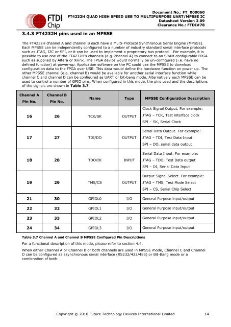
3.4.3 <strong>FT4232H</strong> pins used in an MPSSE<br />
The <strong>FT4232H</strong> channel A and channel B each have a Multi-Protocol Synchronous Serial Engine (MPSSE).<br />
Each MPSSE can be independently configured to a number of industry standard serial interface protocols<br />
such as JTAG, I2C or SPI, or it can be used to implement a proprietary bus protocol. For example, it is<br />
possible to use one of the <strong>FT4232H</strong>’s channels (e.g. channel A) to connect to an SRAM configurable FPGA<br />
such as supplied by Altera or Xilinx. The FPGA device would normally be un-configured (i.e. have no<br />
defined function) at power-up. Application software on the PC could use the MPSSE to download<br />
configuration data to the FPGA over USB. This data would define the hardware function on power up. The<br />
other MPSSE channel (e.g. channel B) would be available for another serial interface function while<br />
channel C and channel D can be configured as UART or bit-bang mode. Alternatively each MPSSE can be<br />
used to control a number of GPIO pins. When configured in this mode, the pins used and the descriptions<br />
of the signals are shown in Table 3.7<br />
Channel A<br />
Pin No.<br />
Channel B<br />
Pin No.<br />
Name Type MPSSE Configuration Description<br />
Clock Signal Output. For example:<br />
16 26 TCK/SK OUTPUT<br />
JTAG – TCK, Test interface clock<br />
SPI – SK, Serial Clock<br />
Serial Data Output. For example:<br />
17 27 TDI/DO OUTPUT<br />
JTAG – TDI, Test Data Input<br />
SPI – DO, serial data output<br />
Serial Data Input. For example:<br />
18 28 TDO/DI INPUT<br />
JTAG – TDO, Test Data output<br />
SPI – DI, Serial Data Input<br />
Output Signal Select. For example:<br />
19 29 TMS/CS OUTPUT<br />
JTAG – TMS, Test Mode Select<br />
SPI – CS, Serial Chip Select<br />
21 30 GPIOL0 I/O General Purpose input/output<br />
22 32 GPIOL1 I/O General Purpose input/output<br />
23 33 GPIOL2 I/O General Purpose input/output<br />
24 34 GPIOL3 I/O General Purpose input/output<br />
Table 3.7 Channel A and Channel B MPSSE Configured Pin Descriptions<br />
For a functional description of this mode, please refer to section 4.4.<br />
When either Channel A or Channel B or both channels are used in MPSSE mode, Channel C and Channel<br />
D can be configured as asynchronous serial interface (RS232/422/485) or Bit-Bang mode or a<br />
combination of both.<br />
Copyright © 2010 <strong>Future</strong> <strong>Technology</strong> <strong>Devices</strong> <strong>International</strong> Limited 14