
You also want an ePaper? Increase the reach of your titles
YUMPU automatically turns print PDFs into web optimized ePapers that Google loves.
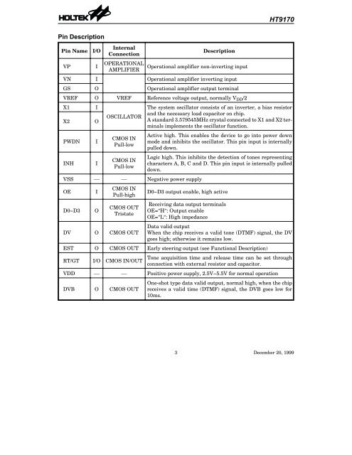
<strong>HT9170</strong><br />
Pin Description<br />
Pin Name<br />
I/O<br />
Internal<br />
Connection<br />
Description<br />
VP I<br />
OPERATIONAL<br />
AMPLIFIER<br />
Operational amplifier non-inverting input<br />
VN I Operational amplifier inverting input<br />
GS O Operational amplifier output terminal<br />
VREF O VREF Reference voltage output, normally V DD /2<br />
X1<br />
X2<br />
PWDN<br />
INH<br />
I<br />
O<br />
I<br />
I<br />
OSCILLATOR<br />
CMOS IN<br />
Pull-low<br />
CMOS IN<br />
Pull-low<br />
VSS Negative power supply<br />
OE<br />
D0~D3<br />
I<br />
O<br />
CMOS IN<br />
Pull-high<br />
CMOS OUT<br />
Tristate<br />
The system oscillator consists of an inverter, a bias resistor<br />
and the necessary load capacitor on chip.<br />
A standard 3.579545MHz crystal connected to X1 and X2 terminals<br />
implements the oscillator function.<br />
Active high. This enables the device to go into power down<br />
mode and inhibits the oscillator. This pin input is internally<br />
pulled down.<br />
Logic high. This inhibits the detection of tones representing<br />
characters A, B, C and D. This pin input is internally pulled<br />
down.<br />
D0~D3 output enable, high active<br />
Receiving data output terminals<br />
OE=H: Output enable<br />
OE=L: High impedance<br />
DV O CMOS OUT<br />
Data valid output<br />
When the chip receives a valid tone (<strong>DTMF</strong>) signal, the DV<br />
goes high; otherwise it remains low.<br />
EST O CMOS OUT Early steering output (see Functional Description)<br />
RT/GT I/O CMOS IN/OUT<br />
Tone acquisition time and release time can be set through<br />
connection with external resistor and capacitor.<br />
VDD Positive power supply, 2.5V~5.5V for normal operation<br />
DVB O CMOS OUT<br />
One-shot type data valid output, normal high, when the chip<br />
receives a valid time (<strong>DTMF</strong>) signal, the DVB goes low for<br />
10ms.<br />
3 December 20, 1999