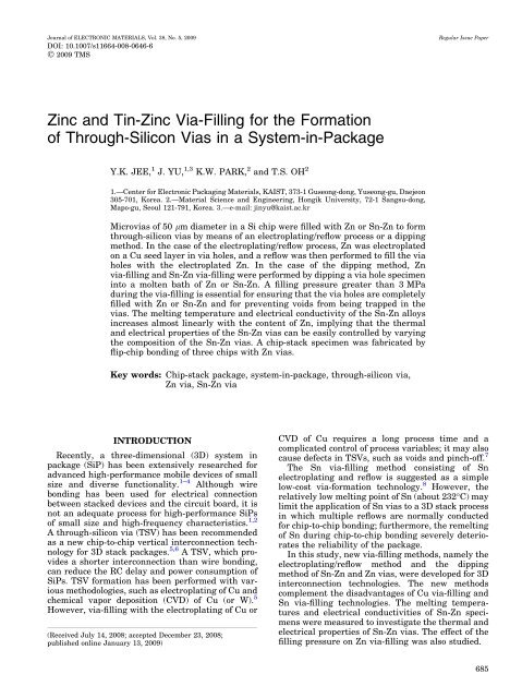
Zinc and Tin-Zinc Via-Filling for the Formation of Through ... - KAIST
Zinc and Tin-Zinc Via-Filling for the Formation of Through ... - KAIST
Zinc and Tin-Zinc Via-Filling for the Formation of Through ... - KAIST

You also want an ePaper? Increase the reach of your titles
YUMPU automatically turns print PDFs into web optimized ePapers that Google loves.
Journal <strong>of</strong> ELECTRONIC MATERIALS, Vol. 38, No. 5, 2009<br />
DOI: 10.1007/s11664-008-0646-6<br />
Ó 2009 TMS<br />
Regular Issue Paper<br />
<strong>Zinc</strong> <strong>and</strong> <strong>Tin</strong>-<strong>Zinc</strong> <strong>Via</strong>-<strong>Filling</strong> <strong>for</strong> <strong>the</strong> <strong>Formation</strong><br />
<strong>of</strong> <strong>Through</strong>-Silicon <strong>Via</strong>s in a System-in-Package<br />
Y.K. JEE, 1 J. YU, 1,3 K.W. PARK, 2 <strong>and</strong> T.S. OH 2<br />
1.—Center <strong>for</strong> Electronic Packaging Materials, <strong>KAIST</strong>, 373-1 Guseong-dong, Yuseong-gu, Daejeon<br />
305-701, Korea. 2.—Material Science <strong>and</strong> Engineering, Hongik University, 72-1 Sangsu-dong,<br />
Mapo-gu, Seoul 121-791, Korea. 3.—e-mail: jinyu@kaist.ac.kr<br />
Microvias <strong>of</strong> 50 lm diameter in a Si chip were filled with Zn or Sn-Zn to <strong>for</strong>m<br />
through-silicon vias by means <strong>of</strong> an electroplating/reflow process or a dipping<br />
method. In <strong>the</strong> case <strong>of</strong> <strong>the</strong> electroplating/reflow process, Zn was electroplated<br />
on a Cu seed layer in via holes, <strong>and</strong> a reflow was <strong>the</strong>n per<strong>for</strong>med to fill <strong>the</strong> via<br />
holes with <strong>the</strong> electroplated Zn. In <strong>the</strong> case <strong>of</strong> <strong>the</strong> dipping method, Zn<br />
via-filling <strong>and</strong> Sn-Zn via-filling were per<strong>for</strong>med by dipping a via hole specimen<br />
into a molten bath <strong>of</strong> Zn or Sn-Zn. A filling pressure greater than 3 MPa<br />
during <strong>the</strong> via-filling is essential <strong>for</strong> ensuring that <strong>the</strong> via holes are completely<br />
filled with Zn or Sn-Zn <strong>and</strong> <strong>for</strong> preventing voids from being trapped in <strong>the</strong><br />
vias. The melting temperature <strong>and</strong> electrical conductivity <strong>of</strong> <strong>the</strong> Sn-Zn alloys<br />
increases almost linearly with <strong>the</strong> content <strong>of</strong> Zn, implying that <strong>the</strong> <strong>the</strong>rmal<br />
<strong>and</strong> electrical properties <strong>of</strong> <strong>the</strong> Sn-Zn vias can be easily controlled by varying<br />
<strong>the</strong> composition <strong>of</strong> <strong>the</strong> Sn-Zn vias. A chip-stack specimen was fabricated by<br />
flip-chip bonding <strong>of</strong> three chips with Zn vias.<br />
Key words: Chip-stack package, system-in-package, through-silicon via,<br />
Zn via, Sn-Zn via<br />
INTRODUCTION<br />
Recently, a three-dimensional (3D) system in<br />
package (SiP) has been extensively researched <strong>for</strong><br />
advanced high-per<strong>for</strong>mance mobile devices <strong>of</strong> small<br />
size <strong>and</strong> diverse functionality. 1–4 Although wire<br />
bonding has been used <strong>for</strong> electrical connection<br />
between stacked devices <strong>and</strong> <strong>the</strong> circuit board, it is<br />
not an adequate process <strong>for</strong> high-per<strong>for</strong>mance SiPs<br />
<strong>of</strong> small size <strong>and</strong> high-frequency characteristics. 1,2<br />
A through-silicon via (TSV) has been recommended<br />
as a new chip-to-chip vertical interconnection technology<br />
<strong>for</strong> 3D stack packages. 5,6 A TSV, which provides<br />
a shorter interconnection than wire bonding,<br />
can reduce <strong>the</strong> RC delay <strong>and</strong> power consumption <strong>of</strong><br />
SiPs. TSV <strong>for</strong>mation has been per<strong>for</strong>med with various<br />
methodologies, such as electroplating <strong>of</strong> Cu <strong>and</strong><br />
chemical vapor deposition (CVD) <strong>of</strong> Cu (or W). 5<br />
However, via-filling with <strong>the</strong> electroplating <strong>of</strong> Cu or<br />
(Received July 14, 2008; accepted December 23, 2008;<br />
published online January 13, 2009)<br />
CVD <strong>of</strong> Cu requires a long process time <strong>and</strong> a<br />
complicated control <strong>of</strong> process variables; it may also<br />
cause defects in TSVs, such as voids <strong>and</strong> pinch-<strong>of</strong>f. 7<br />
The Sn via-filling method consisting <strong>of</strong> Sn<br />
electroplating <strong>and</strong> reflow is suggested as a simple<br />
low-cost via-<strong>for</strong>mation technology. 8 However, <strong>the</strong><br />
relatively low melting point <strong>of</strong> Sn (about 232°C) may<br />
limit <strong>the</strong> application <strong>of</strong> Sn vias to a 3D stack process<br />
in which multiple reflows are normally conducted<br />
<strong>for</strong> chip-to-chip bonding; fur<strong>the</strong>rmore, <strong>the</strong> remelting<br />
<strong>of</strong> Sn during chip-to-chip bonding severely deteriorates<br />
<strong>the</strong> reliability <strong>of</strong> <strong>the</strong> package.<br />
In this study, new via-filling methods, namely <strong>the</strong><br />
electroplating/reflow method <strong>and</strong> <strong>the</strong> dipping<br />
method <strong>of</strong> Sn-Zn <strong>and</strong> Zn vias, were developed <strong>for</strong> 3D<br />
interconnection technologies. The new methods<br />
complement <strong>the</strong> disadvantages <strong>of</strong> Cu via-filling <strong>and</strong><br />
Sn via-filling technologies. The melting temperatures<br />
<strong>and</strong> electrical conductivities <strong>of</strong> Sn-Zn specimens<br />
were measured to investigate <strong>the</strong> <strong>the</strong>rmal <strong>and</strong><br />
electrical properties <strong>of</strong> Sn-Zn vias. The effect <strong>of</strong> <strong>the</strong><br />
filling pressure on Zn via-filling was also studied.<br />
685
686<br />
Jee, Yu, Park, <strong>and</strong> Oh<br />
EXPERIMENTAL PROCEDURE<br />
<strong>Via</strong> holes <strong>of</strong> 50 lm diameter, 150 lm depth, <strong>and</strong><br />
150 lm pitch were <strong>for</strong>med on a 550-lm-thick p-type<br />
(100) Si wafer by using deep reactive-ion etching.<br />
On <strong>the</strong> surface <strong>of</strong> <strong>the</strong> Si wafer <strong>and</strong> via holes, a SiO 2<br />
layer <strong>of</strong> 0.3 lm thickness was deposited by means <strong>of</strong><br />
<strong>the</strong>rmal oxidation as an insulation layer. Subsequently,<br />
Ta/Cu (270 nm/0.5 lm thick) films were<br />
<strong>for</strong>med on <strong>the</strong> wall <strong>and</strong> bottom <strong>of</strong> <strong>the</strong> via holes by<br />
means <strong>of</strong> ionized metal plasma sputtering.<br />
Schematic illustrations <strong>of</strong> Zn via-filling by means<br />
<strong>of</strong> a combined electroplating <strong>and</strong> reflow method are<br />
shown in Fig. 1a. The via holes were partially filled<br />
with Zn by <strong>the</strong> electroplating <strong>of</strong> Zn in a Zn bath <strong>of</strong><br />
zinc chloride (60 g/L), potassium chloride (150 g/L),<br />
boric acid (28 g/L), Unizinc ACZ 552 (humectant,<br />
40 mL/L), <strong>and</strong> Unizinc ACZ 554 (brightener, 2 mL/L).<br />
The electroplating current density was varied<br />
from 5 mA/cm 2 to 20 mA/cm 2 <strong>and</strong> <strong>the</strong> plating time<br />
was changed in a range <strong>of</strong> 60 min to 120 min to<br />
investigate how <strong>the</strong> electroplating conditions affect<br />
<strong>the</strong> Zn via-filling. After <strong>the</strong> electroplating <strong>of</strong> Zn,<br />
<strong>the</strong> specimen was put in an autoclave <strong>and</strong> maintained<br />
at 430°C, which is 10°C higher than <strong>the</strong><br />
melting point <strong>of</strong> Zn (about 421°C) <strong>for</strong> complete<br />
melting <strong>of</strong> <strong>the</strong> Zn, under a pressure <strong>of</strong> 0 MPa to<br />
3 MPa <strong>for</strong> 60 s.<br />
<strong>Via</strong>-filling was also conducted by dipping a via<br />
hole specimen into a bath <strong>of</strong> molten Sn-xZn<br />
(x = 20 wt.%, 30 wt.%, <strong>and</strong> 100 wt.%) as shown in<br />
Fig. 1b. Granules <strong>of</strong> high-purity (99.99%) Sn <strong>and</strong> Zn<br />
were charged in a crucible <strong>and</strong> melted at 430°C to<br />
<strong>for</strong>m <strong>the</strong> molten Sn-xZn, <strong>and</strong> <strong>the</strong> relative amounts <strong>of</strong><br />
<strong>the</strong> Sn <strong>and</strong> Zn granules were weighed to <strong>the</strong><br />
appropriate amounts be<strong>for</strong>e being charged in <strong>the</strong><br />
crucible. A via hole specimen was fixed at <strong>the</strong> holder<br />
<strong>and</strong> immersed in <strong>the</strong> Sn-xZn crucible under a certain<br />
pressure (0 MPa to 4 MPa) controlled by N 2<br />
gas. Finally, <strong>the</strong> specimen was pulled out <strong>of</strong> <strong>the</strong> bath<br />
<strong>and</strong> cooled under <strong>the</strong> N 2 gas pressure.<br />
After <strong>the</strong> via-filling process, chip stacking was<br />
conducted as shown in Fig. 2. Chemical mechanical<br />
Fig. 1. Schematic illustrations <strong>of</strong> via-filling using (a) <strong>the</strong> electroplating/reflow process, <strong>and</strong> (b) <strong>the</strong> dipping process.
<strong>Zinc</strong> <strong>and</strong> <strong>Tin</strong>-<strong>Zinc</strong> <strong>Via</strong>-<strong>Filling</strong> <strong>for</strong> <strong>the</strong> <strong>Formation</strong> <strong>of</strong> <strong>Through</strong>-Silicon <strong>Via</strong>s in a System-in-Package 687<br />
Fig. 2. The process flow <strong>of</strong> chip stacking <strong>for</strong> 3D interconnection.<br />
polishing <strong>and</strong> backside grinding were per<strong>for</strong>med on<br />
<strong>the</strong> Si wafer until <strong>the</strong> wafer was 100 lm thick. The<br />
interconnections between chips were <strong>for</strong>med by <strong>the</strong><br />
fabrication <strong>of</strong> Cu/Sn bumps <strong>of</strong> 70 lm diameter above<br />
<strong>the</strong> Zn vias. The fabrication <strong>of</strong> <strong>the</strong> bumps involved a<br />
process <strong>of</strong> electroplating 10-lm-thick Cu <strong>and</strong> 2-lmthick<br />
Sn after <strong>the</strong> deposition <strong>of</strong> a Ti/Cu (10 nm/<br />
100 nm thick) seed layer. For <strong>the</strong> fabrication <strong>of</strong> a<br />
stacked package, three chips with Zn vias were<br />
aligned one over ano<strong>the</strong>r on an alumina substrate at<br />
250°C with 100 N <strong>for</strong> 2 min after <strong>the</strong> dispensation <strong>of</strong><br />
a nonconductive adhesive.<br />
The liquidus temperatures <strong>of</strong> <strong>the</strong> Sn-xZn<br />
(x = 0 wt.% to 100 wt.%) alloys were measured by<br />
means <strong>of</strong> differential scanning calorimetry, <strong>and</strong> <strong>the</strong><br />
electrical conductivities <strong>of</strong> <strong>the</strong> Sn-xZn alloys were<br />
also evaluated at room temperature with <strong>the</strong> aid <strong>of</strong> a<br />
four-point probe (Suss PM5 probe station) with bulk<br />
Sn-Zn specimens (10 mm 9 10 mm 9 5 mm).<br />
Microstructural analysis was conducted by means<br />
<strong>of</strong> scanning electron microscopy (SEM) after crosssectioning<br />
<strong>the</strong> Si wafers with <strong>the</strong> Sn-xZn vias <strong>and</strong><br />
<strong>the</strong> stacked package specimens. The compositions <strong>of</strong><br />
<strong>the</strong> phases <strong>for</strong>med in <strong>the</strong> Sn-xZn vias <strong>and</strong> <strong>the</strong> Cu-Sn<br />
bumps were identified by means <strong>of</strong> energy-dispersive<br />
spectroscopy.<br />
RESULTS AND DISCUSSION<br />
The liquidus temperatures <strong>and</strong> <strong>the</strong> electrical <strong>and</strong><br />
<strong>the</strong>rmal conductivities <strong>of</strong> <strong>the</strong> Sn-Zn alloys are presented<br />
in Table I. It can be seen that variations in<br />
<strong>the</strong> liquidus temperatures <strong>of</strong> <strong>the</strong> Sn-Zn specimens<br />
are very consistent with <strong>the</strong> reported data. 9 The<br />
electrical conductivities <strong>of</strong> Sn-Zn specimens<br />
increase with <strong>the</strong> amount <strong>of</strong> Zn, a phenomenon<br />
attributed to <strong>the</strong> fact that <strong>the</strong> electrical conductivity<br />
<strong>of</strong> Zn (0.169 (lXcm) 1 ) is higher than that <strong>of</strong> Sn<br />
(0.082 (lXcm) 1 ). The <strong>the</strong>rmal conductivities <strong>of</strong><br />
<strong>the</strong> studied Sn-Zn alloys, which were obtained from<br />
<strong>the</strong> data <strong>of</strong> <strong>the</strong> electrical conductivities <strong>of</strong> <strong>the</strong>se alloys<br />
by using <strong>the</strong> Wiedemann–Franz law <strong>and</strong> <strong>the</strong><br />
Lorenz number (2.45 9 10 8 WX/K 2 ), 10 also increased<br />
with <strong>the</strong> content <strong>of</strong> Zn. Because <strong>the</strong> <strong>the</strong>rmal<br />
conductivity <strong>of</strong> Si is 148 W/m K, 10 <strong>the</strong> Sn-Zn vias <strong>of</strong><br />
high Zn content have <strong>the</strong> advantages <strong>of</strong> a low<br />
<strong>the</strong>rmal expansion mismatch with Si <strong>and</strong> a high<br />
heat transfer capacity. However, <strong>the</strong> Sn-Zn vias <strong>of</strong><br />
high Zn content have high liquidus temperatures<br />
<strong>and</strong> may have a drawback in terms <strong>of</strong> <strong>the</strong> via-filling<br />
process. Thus, <strong>the</strong> optimum composition <strong>of</strong> Sn-Zn<br />
vias should be determined by a trade-<strong>of</strong>f between<br />
<strong>the</strong>se two aspects.<br />
Table I. Physical Properties <strong>of</strong> <strong>the</strong> Sn-Zn Alloys with Various Zn Contents<br />
Zn Content in Sn-Zn<br />
Alloy (wt.%)<br />
Liquidus<br />
Temperature (°C)<br />
Electrical Conductivity<br />
(1/lX cm) at Room Temperature<br />
Thermal Conductivity<br />
(W/m K) at Room Temperature<br />
0 232.1 8.5 ± 0.1 62.5 ± 0.9<br />
10 208 9.2 ± 0.2 67.6 ± 1.4<br />
20 232 10.5 ± 0.16 77.2 ± 1.1<br />
40 307 11.2 ± 0.2 82.3 ± 1.3<br />
60 345 12.3 ± 0.2 90.4 ± 1.1<br />
80 370 14.0 ± 0.2 102.9 ± 1.5<br />
100 420 17.2 ± 0.2 126.4 ± 1.5
688<br />
Jee, Yu, Park, <strong>and</strong> Oh<br />
Fig. 4. Optical micrographs <strong>of</strong> Zn vias filled by electroplating<br />
(5 mA/cm 2 , 120 min) <strong>and</strong> reflow (430°C, 1 min): (a) without a filling<br />
pressure <strong>and</strong> (b) with a filling pressure <strong>of</strong> 3 MPa.<br />
Fig. 3. SEM micrographs <strong>of</strong> <strong>the</strong> Zn layers electroplated into via holes<br />
at (a) 20 mA/cm 2 <strong>for</strong> 60 min <strong>and</strong> (b) 5 mA/cm 2 <strong>for</strong> 120 min.<br />
SEM micrographs <strong>of</strong> <strong>the</strong> Zn layer electroplated<br />
into <strong>the</strong> via holes at a current density <strong>of</strong> 20 mA/cm 2<br />
<strong>for</strong> 60 min are shown in Fig. 3. A pinch-<strong>of</strong>f can be<br />
observed near <strong>the</strong> via mouth, as illustrated in<br />
Fig. 3a, because <strong>the</strong> plating rate was higher, with a<br />
faster charge <strong>and</strong> mass transfer rate, near <strong>the</strong> via<br />
mouth than at <strong>the</strong> via bottom. 7 With such a pinch<strong>of</strong>f<br />
<strong>for</strong>mation, it would be difficult to fill <strong>the</strong> via holes<br />
with Zn even with a reflow process because <strong>the</strong><br />
blocking area (pinch-<strong>of</strong>f) hinders <strong>the</strong> flow <strong>of</strong> molten<br />
Zn into <strong>the</strong> via holes during <strong>the</strong> reflow process. The<br />
electroplated pinch-<strong>of</strong>f was eliminated by fixing <strong>the</strong><br />
current density <strong>and</strong> duration <strong>of</strong> <strong>the</strong> Zn electroplating<br />
at 5 mA/cm 2 <strong>and</strong> 120 min, respectively, <strong>and</strong> by<br />
uni<strong>for</strong>mly electroplating <strong>the</strong> Zn layer over <strong>the</strong> Cu<br />
layer as shown in Fig. 3b instead <strong>of</strong> <strong>for</strong>ming a pinch<strong>of</strong>f<br />
near <strong>the</strong> via mouth. The probability <strong>of</strong> <strong>the</strong> pinch<strong>of</strong>f<br />
<strong>for</strong>mation becomes lower when <strong>the</strong> density <strong>of</strong> <strong>the</strong><br />
electroplating current decreases due to <strong>the</strong> reduced<br />
current crowding at <strong>the</strong> via mouth <strong>and</strong> <strong>the</strong> less<br />
significant mass transport limitation toward <strong>the</strong> via<br />
bottom. 7 In this case, Zn flowed into <strong>the</strong> via holes<br />
smoothly during a reflow <strong>of</strong> Zn. However, <strong>the</strong> via<br />
holes cannot be completely filled solely by means <strong>of</strong><br />
<strong>the</strong> electroplating/reflow process but only when a<br />
filling pressure is applied during <strong>the</strong> reflow <strong>and</strong><br />
cooling steps <strong>of</strong> Zn.<br />
Figure 4 clearly illustrates <strong>the</strong> filling pressure<br />
effect on via-filling during a reflow <strong>of</strong> electroplated<br />
Zn. Optical microscopy was used instead <strong>of</strong> SEM so<br />
that <strong>the</strong> existence <strong>of</strong> voids in <strong>the</strong> vias could be<br />
clearly observed. Without any filling pressure,<br />
numerous voids are trapped in <strong>the</strong> Zn vias after <strong>the</strong><br />
Zn reflow process, as shown in Fig. 4a. On <strong>the</strong> o<strong>the</strong>r<br />
h<strong>and</strong>, <strong>the</strong> application <strong>of</strong> 3 MPa <strong>of</strong> pressure during<br />
<strong>the</strong> reflow process prevents <strong>the</strong> <strong>for</strong>mation <strong>of</strong> voids in<br />
<strong>the</strong> Zn vias, as illustrated in Fig. 4b. The trapping <strong>of</strong><br />
voids in <strong>the</strong> vias can be explained by a mechanism <strong>of</strong><br />
pore <strong>for</strong>mation. 11,12 During <strong>the</strong> reflow process, <strong>the</strong><br />
liquid Zn flows into <strong>the</strong> via holes <strong>and</strong> <strong>the</strong> Zn vapor<br />
acts as a barrier against <strong>the</strong> surrounding gases.<br />
None<strong>the</strong>less, <strong>the</strong> surrounding gases are diffused<br />
into <strong>the</strong> liquid Zn during <strong>the</strong> cooling process<br />
because, in accordance with <strong>the</strong> Clausius–Clapeyron<br />
relation, <strong>the</strong>re is a significant reduction in <strong>the</strong> vapor<br />
pressure <strong>of</strong> Zn. The gases <strong>the</strong>n accumulate in <strong>the</strong> Zn<br />
vias, causing <strong>the</strong> entrapment <strong>of</strong> voids. However, <strong>the</strong><br />
internal pressure <strong>of</strong> <strong>the</strong> liquid Zn increases when<br />
pressure is applied. This prevents <strong>the</strong> gases from<br />
being diffused into <strong>the</strong> liquid Zn during <strong>the</strong> solidification<br />
process <strong>and</strong>, as a result, no voids are<br />
<strong>for</strong>med. 11,12 Note also that <strong>the</strong> pressure accelerates<br />
<strong>the</strong> infiltration <strong>of</strong> Zn into <strong>the</strong> via holes.<br />
<strong>Via</strong>-filling by means <strong>of</strong> <strong>the</strong> dipping method was<br />
also examined <strong>and</strong> compared with <strong>the</strong> electroplating/reflow<br />
process. For <strong>the</strong> dipping method, <strong>the</strong><br />
composition <strong>of</strong> <strong>the</strong> Sn-Zn vias can be easily controlled<br />
just by changing <strong>the</strong> Sn-Zn bath composition.<br />
However, pressure is also essential <strong>for</strong> ensuring <strong>the</strong><br />
vias are completely filled with a Sn-Zn alloy. The<br />
effect <strong>of</strong> pressure on <strong>the</strong> Sn-Zn filling behavior was<br />
also confirmed, as shown in Fig. 6, by varying <strong>the</strong><br />
filling pressure during <strong>the</strong> dipping process. The vias<br />
remain unfilled when <strong>the</strong> applied pressure is 0 MPa<br />
to 2 MPa (Fig. 5a–d) but, as shown in Fig. 5e, <strong>the</strong>y<br />
are completely filled (without voids) when <strong>the</strong><br />
applied pressure is 4 MPa. When a via specimen is<br />
dipped into a molten Sn-Zn bath, <strong>the</strong> liquid Sn-Zn<br />
covers <strong>the</strong> entire surface <strong>of</strong> <strong>the</strong> specimen but does<br />
not flow into <strong>the</strong> via holes due to <strong>the</strong> surface tension<br />
<strong>of</strong> <strong>the</strong> liquid Sn-Zn; hence, air is trapped in <strong>the</strong> via<br />
holes. Without any filling pressure, <strong>the</strong> liquid Sn-Zn<br />
is prevented from flowing into <strong>the</strong> via holes, as<br />
shown in Fig. 5a. When <strong>the</strong> applied pressure is
<strong>Zinc</strong> <strong>and</strong> <strong>Tin</strong>-<strong>Zinc</strong> <strong>Via</strong>-<strong>Filling</strong> <strong>for</strong> <strong>the</strong> <strong>Formation</strong> <strong>of</strong> <strong>Through</strong>-Silicon <strong>Via</strong>s in a System-in-Package 689<br />
Fig. 5. Effect <strong>of</strong> filling pressure <strong>of</strong> (a) 0 MPa, (b) 0.5 MPa, (c) 1 MPa, (d) 2 MPa, <strong>and</strong> (e) 4 MPa on <strong>the</strong> occurrence <strong>of</strong> voids in Sn-30Zn vias<br />
<strong>for</strong>med by <strong>the</strong> dipping method.<br />
Unfilled volume / initial volume ratio<br />
1.0<br />
0.8<br />
0.6<br />
0.4<br />
0.2<br />
0.0<br />
0 1 2 3 4<br />
Applied pressure (MPa)<br />
Fig. 6. Unfilled volume ratio in <strong>the</strong> Sn-30Zn vias <strong>for</strong>med by <strong>the</strong> dipping<br />
process with variation <strong>of</strong> <strong>the</strong> filling pressure.<br />
increasedto2MPa,<strong>the</strong>reisanincreasein<strong>the</strong>volume<br />
ratio <strong>of</strong> <strong>the</strong> filled Sn-Zn in <strong>the</strong> via holes but <strong>the</strong> via<br />
holes are not completely filled (Fig. 5b–d). However,<br />
as shown in Fig. 5e, <strong>the</strong> via holes are completely<br />
filled with Sn-Zn when <strong>the</strong> pressure is 4 MPa. The<br />
correlation between <strong>the</strong> pressure <strong>and</strong> <strong>the</strong> filling <strong>of</strong><br />
Sn-Zn is clearly demonstrated in Fig. 6, that is, <strong>the</strong><br />
unfilled volume ratio is reduced when <strong>the</strong> applied<br />
pressure is increased during <strong>the</strong> via-filling process.<br />
Cross-sectional SEM images <strong>of</strong> <strong>the</strong> vias filled with<br />
Zn <strong>and</strong> Sn-Zn under 3 MPa are presented in Fig. 7a<br />
<strong>and</strong> b. As shown in Fig. 7a, <strong>the</strong> vias are completely<br />
filled with Zn <strong>and</strong> <strong>the</strong>re are no intermetallic compounds<br />
(IMCs) between <strong>the</strong> Zn <strong>and</strong> <strong>the</strong> seed Cu.<br />
During <strong>the</strong> filling process, <strong>the</strong> 100-nm-thick Cu seed<br />
layer was completely dissolved into <strong>the</strong> Zn liquid.<br />
The calculated amount <strong>of</strong> dissolved Cu was about<br />
0.05 wt.%, which is much less than <strong>the</strong> solubility <strong>of</strong><br />
Cu in Zn (about 2.8 wt.%); hence, no IMCs <strong>for</strong>med in<br />
<strong>the</strong> Zn vias. In Fig. 7b, <strong>the</strong> via holes are also completely<br />
filled with Sn-Zn (80 wt.%:20 wt.%). At room<br />
temperature, large platelets <strong>of</strong> Zn precipitates are<br />
dispersed in <strong>the</strong> Sn matrix due to <strong>the</strong> slight solubility<br />
<strong>of</strong> Sn in Zn <strong>and</strong> vice versa. Most <strong>of</strong> <strong>the</strong> Zn<br />
precipitation occurs at <strong>the</strong> wall <strong>of</strong> <strong>the</strong> vias, as shown<br />
in Fig. 7b, possibly due to <strong>the</strong> heterogeneous nucleation<br />
<strong>of</strong> Zn during <strong>the</strong> cooling process at <strong>the</strong> via wall<br />
<strong>of</strong> high surface energy. As mentioned, <strong>the</strong> relative<br />
quantities <strong>of</strong> Sn <strong>and</strong> Zn can be varied by controlling<br />
<strong>the</strong> weight <strong>of</strong> <strong>the</strong> Sn <strong>and</strong> Zn elements in <strong>the</strong> molten<br />
Sn-Zn bath. This type <strong>of</strong> control can yield desirable<br />
via properties, particularly with regard to <strong>the</strong> melting<br />
point <strong>and</strong> coefficient <strong>of</strong> <strong>the</strong>rmal expansion, as<br />
well as <strong>the</strong> <strong>the</strong>rmal <strong>and</strong> electrical conductivities.<br />
After <strong>the</strong> via-filling process, three-chip stacking<br />
was conducted by flip-chip bonding <strong>of</strong> planar-type<br />
Cu/Sn bumps at 250°C <strong>for</strong> 120 s under 100 N, as<br />
shown in Fig. 8a. A nonconductive adhesive was<br />
applied to each chip be<strong>for</strong>e <strong>the</strong> flip-chip bonding. As<br />
illustrated in Fig. 8b, <strong>the</strong> chip-stacked interface was<br />
composed <strong>of</strong> Cu 3 Sn/Cu 6 Sn 5 /Cu 3 Sn layers. In <strong>the</strong><br />
case <strong>of</strong> <strong>the</strong> Cu/Sn bump joints, <strong>the</strong> <strong>for</strong>mation <strong>of</strong><br />
Kirkendall voids raises <strong>the</strong> issue <strong>of</strong> mechanical<br />
reliability during iso<strong>the</strong>rmal aging treatment. The<br />
addition <strong>of</strong> Zn to Sn reportedly suppresses <strong>the</strong> <strong>for</strong>mation<br />
<strong>of</strong> Kirkendall voids due to <strong>the</strong> accumulation<br />
<strong>of</strong> Zn at <strong>the</strong> IMC/Cu interface <strong>and</strong> consequently<br />
increases <strong>the</strong> reliability <strong>of</strong> <strong>the</strong> bump joints. 13 The<br />
Sn-Zn bumps may improve <strong>the</strong> mechanical reliability<br />
<strong>of</strong> <strong>the</strong> bump joints <strong>of</strong> <strong>the</strong> chip-stack specimens.<br />
CONCLUSION<br />
The use <strong>of</strong> electroplating/reflow <strong>and</strong> dipping<br />
methods in Zn <strong>and</strong> Sn-Zn via-filling processes <strong>for</strong><br />
TSVs <strong>of</strong>fers wider process windows <strong>for</strong> chip-stack<br />
packages. The application <strong>of</strong> a current density <strong>of</strong><br />
5 mA/cm 2 <strong>for</strong> 120 min restrained <strong>the</strong> pinch-<strong>of</strong>f near
690<br />
Jee, Yu, Park, <strong>and</strong> Oh<br />
Fig. 7. Cross-sectional SEM micrographs <strong>of</strong> (a) Zn <strong>and</strong> (b) Sn-20Zn vias filled by <strong>the</strong> dipping process with an applied filling pressure <strong>of</strong> 3 MPa.<br />
specimens, chip stacking was successfully conducted<br />
by using a flip-chip bonding process.<br />
Fig. 8. Cross-sectional SEM micrographs <strong>of</strong> (a) a three-chip-stacked<br />
specimen with Zn vias <strong>and</strong> (b) a Cu-Sn bump joint.<br />
<strong>the</strong> via mouth during <strong>the</strong> electroplating <strong>of</strong> Zn,<br />
enabling <strong>the</strong> electroplated Zn to flow into <strong>the</strong> via holes<br />
during <strong>the</strong> subsequent reflow process. <strong>Via</strong>-filling<br />
can be successfully achieved by dipping a via hole<br />
specimen into a molten Sn-Zn bath. In both cases,<br />
a pressure <strong>of</strong> 3 MPa or more should be applied<br />
during <strong>the</strong> filling <strong>and</strong> cooling steps. With <strong>the</strong> Zn via<br />
ACKNOWLEDGEMENT<br />
This work was supported by <strong>the</strong> Center <strong>for</strong> Electronic<br />
Packaging Materials (ERC) <strong>of</strong> MOST/KOSEF<br />
(Grant #R11-2000-085-08001-0).<br />
REFERENCES<br />
1. S.F. Al-Sarawi, D. Abbott, <strong>and</strong> P. Franzon, IEEE Trans.<br />
Comput. 21, 2 (1998).<br />
2. R.E. Terrill, Proceedings <strong>of</strong> <strong>the</strong> International Conference on<br />
Multichip Modules, Denver, CO, 1995, p. 7.<br />
3. S. Sheng, A. Ch<strong>and</strong>rakasan, <strong>and</strong> R.W. Brodersen, IEEE<br />
Commun. Mag. 30, 64 (1992). doi:10.1109/35.210358.<br />
4. R. Crowley, Technical Report, Techsearch Int. Inc. Austin,<br />
TX, 1993, p. 159.<br />
5. K. Takahashi, H. Terao, Y. Tomita, Y. Yamaji, M. Hoshino,<br />
T. Sato, T. Morifuji, M. Sunohara, <strong>and</strong> M. Bonkohara, Jpn.<br />
J. Appl. Phys. 40, 3032 (2001). doi:10.1143/JJAP.40.3032.<br />
6. P. Ramm, D. Bollmann, R. Braun, R. Buchner, U. Cao-Minh,<br />
M. Engelhardt, G. Errmann, <strong>and</strong> W. Weber, Microelectron.<br />
Eng. 37, 39 (1997). doi:10.1016/S0167-9317(97)00092-0.<br />
7. B. Kim, C. Sharbono, T. Ritzdorf, <strong>and</strong> D. Schmauch,<br />
Proceedings <strong>of</strong> <strong>the</strong> Electronics Components Technology<br />
Conference, San Diego, CA, 2006, p. 838.<br />
8. D.M. Jang, C. Ryu, K.Y. Lee, B.H. Cho, J. Kim, T.S. Oh,<br />
W.J. Lee, <strong>and</strong> J. Yu, Proceedings <strong>of</strong> <strong>the</strong> Electronics Components<br />
Technology Conference, Reno, NV, 2007, p. 847.<br />
9. M. Hansen, Constitution <strong>of</strong> Binary Alloys (New York:<br />
McGraw-Hill, 1958), p. 1217.<br />
10. C. Kittel, Introduction to Solid State Physics (New York:<br />
Wiley, 1996), p. 168.<br />
11. A.K. Gupta, B.K. Saxena, S.N. Tiwari, <strong>and</strong> S.L. Malhotra,<br />
J. Mater. Sci. 27, 853 (1992). doi:10.1007/BF01197634.<br />
12. A.F.H. Kaplan, M. Mizutani, S. Katayama, <strong>and</strong> A. Matsunawa,<br />
J. Phys. D Appl. Phys. 35, 1218 (2002).<br />
13. Y.K. Jee, Y.H. Ko, <strong>and</strong> J. Yu, J. Mater. Res. 22, 1879 (2007).<br />
doi:10.1557/jmr.2007.0234.