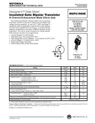
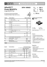
NTE7142 Integrated Circuit +5VâPowered ... - Datasheets
NTE7142 Integrated Circuit +5VâPowered ... - Datasheets
NTE7142 Integrated Circuit +5VâPowered ... - Datasheets

Create successful ePaper yourself
Turn your PDF publications into a flip-book with our unique Google optimized e-Paper software.
<strong>NTE7142</strong><br />
<strong>Integrated</strong> <strong>Circuit</strong><br />
+5V–Powered, Multichannel RS–232 Driver/Receiver<br />
Description:<br />
The <strong>NTE7142</strong> is a multichannel RS–232 driver/receiver in a 16–Lead DIP type package intended for<br />
all EIA/TIA–232E and V.28/V.24 communications interfaces, particularly applications where ±12V is<br />
not available.<br />
Features:<br />
Operate From Single +5V Power Supply<br />
Meet All EIA/TIA–232E and V.28 Specifications<br />
Multiple Drivers and Receivers<br />
3–State Driver and Receiver Outputs<br />
Applications:<br />
Portable Computers<br />
Low–Power Modems<br />
Interface Translation<br />
Battery–Powered RS–232 Systems<br />
Multidrop RS–232 Networks<br />
Absolute Maximum Ratings: (Note 1)<br />
Supply Voltage, V CC . . . . . . . . . . . . . . . . . . . . . . . . . . . . . . . . . . . . . . . . . . . . . . . . . . . . . . . . –0.3V to +6V<br />
Input Voltage, T IN . . . . . . . . . . . . . . . . . . . . . . . . . . . . . . . . . . . . . . . . . . . . . . . . . . . –0.3V to (V CC –0.3V)<br />
Input Voltage, R IN . . . . . . . . . . . . . . . . . . . . . . . . . . . . . . . . . . . . . . . . . . . . . . . . . . . . . . . . . . . . . . . . . ±30V<br />
Output Voltage (Note 2), T OUT . . . . . . . . . . . . . . . . . . . . . . . . . . . . . . . . . . . . . . . . . . . . . . . . . . . . . . ±15V<br />
Output Voltage, R OUT . . . . . . . . . . . . . . . . . . . . . . . . . . . . . . . . . . . . . . . . . . . . . . . . –0.3V to (V CC +0.3V)<br />
Driver/Receiver Output Short <strong>Circuit</strong>ed to GND . . . . . . . . . . . . . . . . . . . . . . . . . . . . . . . . . . Continuous<br />
Continuous Power Dissipation (T A = +70°C), P D . . . . . . . . . . . . . . . . . . . . . . . . . . . . . . . . . . . . . 842mW<br />
Dreate Above +70°C . . . . . . . . . . . . . . . . . . . . . . . . . . . . . . . . . . . . . . . . . . . . . . . . . . 10.53mW/°C<br />
Operating Temperature Range, T opr . . . . . . . . . . . . . . . . . . . . . . . . . . . . . . . . . . . . . . . . . . . 0° to +70°C<br />
Storage Temperature Range, T stg . . . . . . . . . . . . . . . . . . . . . . . . . . . . . . . . . . . . . . . . . . –65° to +160°C<br />
Lead Temperature (During Soldering, 10sec), T L . . . . . . . . . . . . . . . . . . . . . . . . . . . . . . . . . . . . +300°C<br />
Note 1. Stresses beyond those listed under “Absolute Maximum Ratings” may cause permanent<br />
damage to the device. These are stress ratings only, and functional operation of the device<br />
at these or any other conditions beyond those indicated in the operational section of the<br />
specifications is not implied. Exposure to absolute maximum rating conditions for extended<br />
periods may affect device reliability.<br />
Note 2. Input voltage measured with T OUT in high–impedance state, V CC = 0V.
Electrical Characteristics: (V CC = +5V ±10%, T A = 0° to +70°C, C1–C4 = 0.1µF unless otherwise<br />
specified)<br />
Parameter Test Conditions Min Typ Max Unit<br />
RS–232 Transmitter<br />
Output Voltage Swing All transmitter output loaded with 3kΩ to GND ±5 ±8 – V<br />
Input Logic Threshold Low – 1.4 0.85 V<br />
Input Logic Threshold High 2.0 1.4 – V<br />
Logic Pull–Up/Input Current Normal operation – 5 40 µA<br />
Output Leakage Current V CC = 0V, V OUT = ±15V – ±0.01 ±10 µA<br />
Data Rate Normal operation – 200 116 kb/s<br />
Transmitter Output Resistance V CC = V+ = V– = 0V, V OUT = ±2V 300 10M – Ω<br />
Output Short–<strong>Circuit</strong> Current V OUT = 0V ±7 ±22 – mA<br />
RS–232 Receiver<br />
RS–232 Input Voltage Operating<br />
Range<br />
– – ±30 V<br />
RS–232 Input Threshold Low V CC = 5V, R2 IN 0.8 1.3 – V<br />
RS–232 Input Threshold High V CC = 5V, R2 IN – 1.8 2.4 V<br />
RS–232 Input Hysteresis V CC = 5V 0.2 0.5 1.0 V<br />
RS–232 Input Resistance 3 5 7 kΩ<br />
TTL/CMOS Output Voltage Low I OUT = 3.2mA – 0.2 0.4 V<br />
TTL/CMOS Output Voltage High I OUT = –1.0mA 3.5 V CC –0.2 – V<br />
TTL/CMOS Output Short–<strong>Circuit</strong> Sourcing, V OUT = GND –2 –10 – mA<br />
Current<br />
Shrinking, V OUT = V CC 10 30 – mA<br />
TTL/CMOS Output Leakage Current 0V ≤ V OUT ≤ V CC – ±0.05 ±10 µA<br />
Operating Supply Voltage 4.5 – 5.5 V<br />
V CC Supply Current No load – 4 10 mA<br />
Transition Slew Rate<br />
3kΩ load, both inputs – 15 – mA<br />
C L = 50pF to 2500pF, R L = 3kΩ to 7kΩ,<br />
V CC = 5V, T A = +25°C, measured from<br />
+3V to –3V or –3V to +3V<br />
6 12 30 V/µs<br />
Transmitter Propagation Delay t PHLT – 1.3 3.5 µs<br />
TTL to RS–232 (normal operation)<br />
t PLHT – 1.5 3.5 µs<br />
Receiver Propagation Delay t PHLR – 0.5 1.0 µs<br />
RS–232 to TTL (normal operation)<br />
t PLHR – 0.6 1.0 µs<br />
Transmitter + to – Propagation Delay<br />
Difference (normal operation)<br />
Receiver + to – Propagation Delay<br />
Difference (normal operation)<br />
t PHLT – t PLHT – 300 – ns<br />
t PHLR – t PLHR – 100 – ns
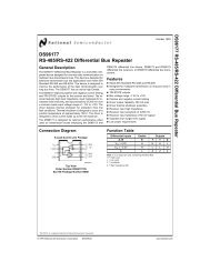
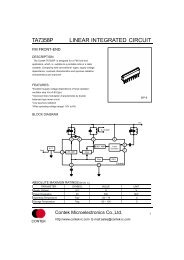
Pin Connection Diagram<br />
Capacitor 1 (+) 1<br />
V+ (+10V) 2<br />
Capacitor 1 (–) 3<br />
Capacitor 2 (+) 4<br />
Capacitor 2 (–) 5<br />
V– (–10V) 6<br />
RS–232 Output 2 7<br />
RS–232 Input 2 8<br />
16<br />
15<br />
14<br />
13<br />
12<br />
11<br />
10<br />
9<br />
V CC<br />
GND<br />
RS–232 Output 1<br />
RS–232 Input 1<br />
TTL/CMOS Out 1<br />
TTL/CMOS In 1<br />
TTL/CMOS In 2<br />
TTL/CMOS Out 2<br />
16 9<br />
1 8<br />
.765 (19.43)<br />
Max<br />
.325 (8.26)<br />
Max<br />
.180 (4.57)<br />
Max<br />
.100 (2.54)<br />
.115 (2.92) Min<br />
.700 (17.78)