cSI PHOTOVOLTAIC SOLUTIONS - Manz
cSI PHOTOVOLTAIC SOLUTIONS - Manz
cSI PHOTOVOLTAIC SOLUTIONS - Manz

You also want an ePaper? Increase the reach of your titles
YUMPU automatically turns print PDFs into web optimized ePapers that Google loves.
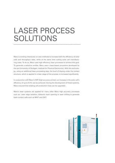
LASER PROCESS<br />
<strong>SOLUTIONS</strong><br />
<strong>Manz</strong> is working intensively on new methods to increase both the efficiency of solar<br />
cells and throughput rates, while at the same time cutting solar cell manufacturing<br />
costs. To do so, <strong>Manz</strong> uses high-efficiency laser processes to achieve this goal.<br />
To generate a selective emitter, <strong>Manz</strong> uses a laser-based procedure developed by<br />
the ipe (University of Stuttgart, Institute for Physical Electronics). With this technology,<br />
using an additional laser-processing step, the level of doping under the contact<br />
structure, which is applied in a later stage of the process, is increased significantly.<br />
In conjunction with <strong>Manz</strong>’s HAP (high accuracy printer), an increase in the solar cell’s<br />
efficiency of up to 0.5% can be achieved. During the development of these systems,<br />
<strong>Manz</strong> ensured that existing cell production lines can be upgraded.<br />
<strong>Manz</strong>’s laser systems are applied for many other <strong>Manz</strong> high accuracy processes<br />
such as: Laser edge isolation, dielectric layer opening or laser drilling to generate<br />
back-contact cells such as MWT and EWT.<br />
Laser Edge Isolation Selective Emitter<br />
LASER EDGE ISOLATION<br />
Edge isolation by laser grooving<br />
High throughput of up to 2,400 wafer/h<br />
Safe wafer handling and lowest breakage rates<br />
Loading/Unloading from/into <strong>Manz</strong> Box/Cassette or alternative carrier<br />
Modular design – available as inline or stand-alone system<br />
Combination of high performance laser process with high precision machine<br />
allows a minimum “dead area” (≤ 100 µm)<br />
SELECTIVE EMITTER<br />
High throughput of up to 2,400 wafer/h<br />
Safe wafer handling – lowest breakage rates<br />
Increase of cell efficiency up to 0.5% in combination with high ohmic emitter<br />
and <strong>Manz</strong> HAP (high accuracy printing)<br />
Loading/Unloading from/into <strong>Manz</strong> Box/Cassette or alternative carrier<br />
Modular design – available as inline or stand-alone system<br />
17<br />
Minimum dead area<br />
of ≤ 100 µm<br />
Lowest breakage rates<br />
Increase cell efficiency up to 0.5%