STMicroelectronics L7806CV datasheet: pdf - Octopart
STMicroelectronics L7806CV datasheet: pdf - Octopart
STMicroelectronics L7806CV datasheet: pdf - Octopart

You also want an ePaper? Increase the reach of your titles
YUMPU automatically turns print PDFs into web optimized ePapers that Google loves.
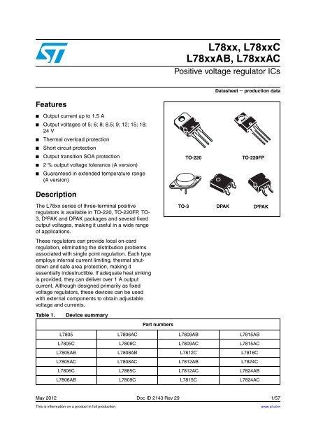
L78xx, L78xxC<br />
L78xxAB, L78xxAC<br />
Positive voltage regulator ICs<br />
Datasheet − production data<br />
Features<br />
■<br />
Output current up to 1.5 A<br />
■ Output voltages of 5; 6; 8; 8.5; 9; 12; 15; 18;<br />
24 V<br />
■<br />
Thermal overload protection<br />
■<br />
Short circuit protection<br />
■<br />
■<br />
Output transition SOA protection<br />
2 % output voltage tolerance (A version)<br />
TO-220<br />
TO-220FP<br />
■<br />
Guaranteed in extended temperature range<br />
(A version)<br />
Description<br />
The L78xx series of three-terminal positive<br />
regulators is available in TO-220, TO-220FP, TO-<br />
3, D²PAK and DPAK packages and several fixed<br />
output voltages, making it useful in a wide range<br />
of applications.<br />
TO-3<br />
DPAK<br />
D²PAK<br />
These regulators can provide local on-card<br />
regulation, eliminating the distribution problems<br />
associated with single point regulation. Each type<br />
employs internal current limiting, thermal shutdown<br />
and safe area protection, making it<br />
essentially indestructible. If adequate heat sinking<br />
is provided, they can deliver over 1 A output<br />
current. Although designed primarily as fixed<br />
voltage regulators, these devices can be used<br />
with external components to obtain adjustable<br />
voltage and currents.<br />
Table 1.<br />
Device summary<br />
Part numbers<br />
L7805 L7806AC L7809AB L7815AB<br />
L7805C L7808C L7809AC L7815AC<br />
L7805AB L7808AB L7812C L7818C<br />
L7805AC L7808AC L7812AB L7824C<br />
L7806C L7885C L7812AC L7824AB<br />
L7806AB L7809C L7815C L7824AC<br />
May 2012 Doc ID 2143 Rev 29 1/57<br />
This is information on a product in full production.<br />
www.st.com<br />
57
Contents<br />
L78xx, L78xxC, L78xxAB, L78xxAC<br />
Contents<br />
1 Diagram . . . . . . . . . . . . . . . . . . . . . . . . . . . . . . . . . . . . . . . . . . . . . . . . . . . 5<br />
2 Pin configuration . . . . . . . . . . . . . . . . . . . . . . . . . . . . . . . . . . . . . . . . . . . 6<br />
3 Maximum ratings . . . . . . . . . . . . . . . . . . . . . . . . . . . . . . . . . . . . . . . . . . . . 7<br />
4 Test circuits . . . . . . . . . . . . . . . . . . . . . . . . . . . . . . . . . . . . . . . . . . . . . . . . 8<br />
5 Electrical characteristics . . . . . . . . . . . . . . . . . . . . . . . . . . . . . . . . . . . . . 9<br />
6 Application information . . . . . . . . . . . . . . . . . . . . . . . . . . . . . . . . . . . . . 28<br />
6.1 Design consideration . . . . . . . . . . . . . . . . . . . . . . . . . . . . . . . . . . . . . . . . 28<br />
7 Typical performance . . . . . . . . . . . . . . . . . . . . . . . . . . . . . . . . . . . . . . . . 37<br />
8 Package mechanical data . . . . . . . . . . . . . . . . . . . . . . . . . . . . . . . . . . . . 39<br />
9 Order codes . . . . . . . . . . . . . . . . . . . . . . . . . . . . . . . . . . . . . . . . . . . . . . 54<br />
10 Revision history . . . . . . . . . . . . . . . . . . . . . . . . . . . . . . . . . . . . . . . . . . . 56<br />
2/57 Doc ID 2143 Rev 29
L78xx, L78xxC, L78xxAB, L78xxAC<br />
List of tables<br />
List of tables<br />
Table 1. Device summary . . . . . . . . . . . . . . . . . . . . . . . . . . . . . . . . . . . . . . . . . . . . . . . . . . . . . . . . . . 1<br />
Table 2. Absolute maximum ratings . . . . . . . . . . . . . . . . . . . . . . . . . . . . . . . . . . . . . . . . . . . . . . . . . . 7<br />
Table 3. Thermal data. . . . . . . . . . . . . . . . . . . . . . . . . . . . . . . . . . . . . . . . . . . . . . . . . . . . . . . . . . . . . 7<br />
Table 4. Electrical characteristics of L7805 . . . . . . . . . . . . . . . . . . . . . . . . . . . . . . . . . . . . . . . . . . . . 9<br />
Table 5. Electrical characteristics of L7805A . . . . . . . . . . . . . . . . . . . . . . . . . . . . . . . . . . . . . . . . . . 10<br />
Table 6. Electrical characteristics of L7806A . . . . . . . . . . . . . . . . . . . . . . . . . . . . . . . . . . . . . . . . . . 11<br />
Table 7. Electrical characteristics of L7808A . . . . . . . . . . . . . . . . . . . . . . . . . . . . . . . . . . . . . . . . . . 12<br />
Table 8. Electrical characteristics of L7809A . . . . . . . . . . . . . . . . . . . . . . . . . . . . . . . . . . . . . . . . . . 13<br />
Table 9. Electrical characteristics of L7812A . . . . . . . . . . . . . . . . . . . . . . . . . . . . . . . . . . . . . . . . . . 14<br />
Table 10. Electrical characteristics of L7815A . . . . . . . . . . . . . . . . . . . . . . . . . . . . . . . . . . . . . . . . . . 15<br />
Table 11. Electrical characteristics of L7824A . . . . . . . . . . . . . . . . . . . . . . . . . . . . . . . . . . . . . . . . . . 16<br />
Table 12. Electrical characteristics of L7805C . . . . . . . . . . . . . . . . . . . . . . . . . . . . . . . . . . . . . . . . . . 17<br />
Table 13. Electrical characteristics of L7806C . . . . . . . . . . . . . . . . . . . . . . . . . . . . . . . . . . . . . . . . . . 18<br />
Table 14. Electrical characteristics of L7808C . . . . . . . . . . . . . . . . . . . . . . . . . . . . . . . . . . . . . . . . . . 19<br />
Table 15. Electrical characteristics of L7885C . . . . . . . . . . . . . . . . . . . . . . . . . . . . . . . . . . . . . . . . . . 20<br />
Table 16. Electrical characteristics of L7809C . . . . . . . . . . . . . . . . . . . . . . . . . . . . . . . . . . . . . . . . . . 21<br />
Table 17. Electrical characteristics of L7810C . . . . . . . . . . . . . . . . . . . . . . . . . . . . . . . . . . . . . . . . . . 22<br />
Table 18. Electrical characteristics of L7812C . . . . . . . . . . . . . . . . . . . . . . . . . . . . . . . . . . . . . . . . . . 23<br />
Table 19. Electrical characteristics of L7815C . . . . . . . . . . . . . . . . . . . . . . . . . . . . . . . . . . . . . . . . . . 24<br />
Table 20. Electrical characteristics of L7818C . . . . . . . . . . . . . . . . . . . . . . . . . . . . . . . . . . . . . . . . . . 25<br />
Table 21. Electrical characteristics of L7820C . . . . . . . . . . . . . . . . . . . . . . . . . . . . . . . . . . . . . . . . . . 26<br />
Table 22. Electrical characteristics of L7824C . . . . . . . . . . . . . . . . . . . . . . . . . . . . . . . . . . . . . . . . . . 27<br />
Table 23. TO-220 mechanical data . . . . . . . . . . . . . . . . . . . . . . . . . . . . . . . . . . . . . . . . . . . . . . . . . . 39<br />
Table 24. TO-220FP mechanical data . . . . . . . . . . . . . . . . . . . . . . . . . . . . . . . . . . . . . . . . . . . . . . . . 44<br />
Table 25. TO-3 mechanical data . . . . . . . . . . . . . . . . . . . . . . . . . . . . . . . . . . . . . . . . . . . . . . . . . . . . 45<br />
Table 26. DPAK mechanical data. . . . . . . . . . . . . . . . . . . . . . . . . . . . . . . . . . . . . . . . . . . . . . . . . . . . 47<br />
Table 27. Tape and reel DPAK mechanical data . . . . . . . . . . . . . . . . . . . . . . . . . . . . . . . . . . . . . . . . 48<br />
Table 28. D²PAK mechanical data . . . . . . . . . . . . . . . . . . . . . . . . . . . . . . . . . . . . . . . . . . . . . . . . . . . 51<br />
Table 29. D²PAK footprint data. . . . . . . . . . . . . . . . . . . . . . . . . . . . . . . . . . . . . . . . . . . . . . . . . . . . . . 52<br />
Table 30. Tape and reel D²PAK mechanical data . . . . . . . . . . . . . . . . . . . . . . . . . . . . . . . . . . . . . . . 53<br />
Table 31. Order codes . . . . . . . . . . . . . . . . . . . . . . . . . . . . . . . . . . . . . . . . . . . . . . . . . . . . . . . . . . . . 54<br />
Table 32. Document revision history . . . . . . . . . . . . . . . . . . . . . . . . . . . . . . . . . . . . . . . . . . . . . . . . . 56<br />
Doc ID 2143 Rev 29 3/57
List of figures<br />
L78xx, L78xxC, L78xxAB, L78xxAC<br />
List of figures<br />
Figure 1. Block diagram . . . . . . . . . . . . . . . . . . . . . . . . . . . . . . . . . . . . . . . . . . . . . . . . . . . . . . . . . . . . 5<br />
Figure 2. Pin connections (top view) . . . . . . . . . . . . . . . . . . . . . . . . . . . . . . . . . . . . . . . . . . . . . . . . . . 6<br />
Figure 3. Schematic diagram . . . . . . . . . . . . . . . . . . . . . . . . . . . . . . . . . . . . . . . . . . . . . . . . . . . . . . . . 6<br />
Figure 4. Application circuits . . . . . . . . . . . . . . . . . . . . . . . . . . . . . . . . . . . . . . . . . . . . . . . . . . . . . . . . 7<br />
Figure 5. DC parameter . . . . . . . . . . . . . . . . . . . . . . . . . . . . . . . . . . . . . . . . . . . . . . . . . . . . . . . . . . . . 8<br />
Figure 6. Load regulation . . . . . . . . . . . . . . . . . . . . . . . . . . . . . . . . . . . . . . . . . . . . . . . . . . . . . . . . . . . 8<br />
Figure 7. Ripple rejection . . . . . . . . . . . . . . . . . . . . . . . . . . . . . . . . . . . . . . . . . . . . . . . . . . . . . . . . . . . 8<br />
Figure 8. Fixed output regulator. . . . . . . . . . . . . . . . . . . . . . . . . . . . . . . . . . . . . . . . . . . . . . . . . . . . . 28<br />
Figure 9. Current regulator. . . . . . . . . . . . . . . . . . . . . . . . . . . . . . . . . . . . . . . . . . . . . . . . . . . . . . . . . 29<br />
Figure 10. Circuit for increasing output voltage . . . . . . . . . . . . . . . . . . . . . . . . . . . . . . . . . . . . . . . . . . 29<br />
Figure 11. Adjustable output regulator (7 to 30 V) . . . . . . . . . . . . . . . . . . . . . . . . . . . . . . . . . . . . . . . . 29<br />
Figure 12. 0.5 to 10 V regulator . . . . . . . . . . . . . . . . . . . . . . . . . . . . . . . . . . . . . . . . . . . . . . . . . . . . . . 30<br />
Figure 13. High current voltage regulator . . . . . . . . . . . . . . . . . . . . . . . . . . . . . . . . . . . . . . . . . . . . . . 30<br />
Figure 14. High output current with short circuit protection . . . . . . . . . . . . . . . . . . . . . . . . . . . . . . . . . 30<br />
Figure 15. Tracking voltage regulator . . . . . . . . . . . . . . . . . . . . . . . . . . . . . . . . . . . . . . . . . . . . . . . . . 31<br />
Figure 16. Split power supply (± 15 V - 1 A) . . . . . . . . . . . . . . . . . . . . . . . . . . . . . . . . . . . . . . . . . . . . 31<br />
Figure 17. Negative output voltage circuit . . . . . . . . . . . . . . . . . . . . . . . . . . . . . . . . . . . . . . . . . . . . . . 32<br />
Figure 18. Switching regulator . . . . . . . . . . . . . . . . . . . . . . . . . . . . . . . . . . . . . . . . . . . . . . . . . . . . . . . 32<br />
Figure 19. High input voltage circuit (configuration 1) . . . . . . . . . . . . . . . . . . . . . . . . . . . . . . . . . . . . . 32<br />
Figure 20. High input voltage circuit (configuration 2) . . . . . . . . . . . . . . . . . . . . . . . . . . . . . . . . . . . . . 33<br />
Figure 21. High output voltage regulator . . . . . . . . . . . . . . . . . . . . . . . . . . . . . . . . . . . . . . . . . . . . . . . 33<br />
Figure 22. High input and output voltage . . . . . . . . . . . . . . . . . . . . . . . . . . . . . . . . . . . . . . . . . . . . . . . 33<br />
Figure 23. Reducing power dissipation with dropping resistor. . . . . . . . . . . . . . . . . . . . . . . . . . . . . . . 34<br />
Figure 24. Remote shutdown. . . . . . . . . . . . . . . . . . . . . . . . . . . . . . . . . . . . . . . . . . . . . . . . . . . . . . . . 34<br />
Figure 25. Power AM modulator (unity voltage gain, I O £ 0.5). . . . . . . . . . . . . . . . . . . . . . . . . . . . . . . 34<br />
Figure 26. Adjustable output voltage with temperature compensation . . . . . . . . . . . . . . . . . . . . . . . . 35<br />
Figure 27. Light controllers (V O(min) = V XX + V BE ) . . . . . . . . . . . . . . . . . . . . . . . . . . . . . . . . . . . . . . . . 35<br />
Figure 28. Protection against input short-circuit with high capacitance loads . . . . . . . . . . . . . . . . . . . 36<br />
Figure 29. Dropout voltage vs. junction temperature . . . . . . . . . . . . . . . . . . . . . . . . . . . . . . . . . . . . . . 37<br />
Figure 30. Peak output current vs. input/output differential voltage. . . . . . . . . . . . . . . . . . . . . . . . . . . 37<br />
Figure 31. Supply voltage rejection vs. frequency . . . . . . . . . . . . . . . . . . . . . . . . . . . . . . . . . . . . . . . . 37<br />
Figure 32. Output voltage vs. junction temperature . . . . . . . . . . . . . . . . . . . . . . . . . . . . . . . . . . . . . . . 37<br />
Figure 33. Output impedance vs. frequency . . . . . . . . . . . . . . . . . . . . . . . . . . . . . . . . . . . . . . . . . . . . 37<br />
Figure 34. Quiescent current vs. junction temp. . . . . . . . . . . . . . . . . . . . . . . . . . . . . . . . . . . . . . . . . . 37<br />
Figure 35. Load transient response . . . . . . . . . . . . . . . . . . . . . . . . . . . . . . . . . . . . . . . . . . . . . . . . . . . 38<br />
Figure 36. Line transient response . . . . . . . . . . . . . . . . . . . . . . . . . . . . . . . . . . . . . . . . . . . . . . . . . . . 38<br />
Figure 37. Quiescent current vs. input voltage . . . . . . . . . . . . . . . . . . . . . . . . . . . . . . . . . . . . . . . . . . 38<br />
Figure 38. Drawing dimension TO-220 (type STD-ST Dual Gauge) . . . . . . . . . . . . . . . . . . . . . . . . . . 40<br />
Figure 39. Drawing dimension TO-220 (type STD-ST Single Gauge) . . . . . . . . . . . . . . . . . . . . . . . . . 41<br />
Figure 40. Drawing dimension tube for TO-220 Dual Gauge (mm.) . . . . . . . . . . . . . . . . . . . . . . . . . . 42<br />
Figure 41. Drawing dimension tube for TO-220 Single Gauge (mm.) . . . . . . . . . . . . . . . . . . . . . . . . . 42<br />
Figure 42. Drawing dimension TO-220FP . . . . . . . . . . . . . . . . . . . . . . . . . . . . . . . . . . . . . . . . . . . . . . 43<br />
Figure 43. Drawing dimension TO-3 . . . . . . . . . . . . . . . . . . . . . . . . . . . . . . . . . . . . . . . . . . . . . . . . . . 45<br />
Figure 44. Drawing dimension DPAK . . . . . . . . . . . . . . . . . . . . . . . . . . . . . . . . . . . . . . . . . . . . . . . . . 46<br />
Figure 45. Drawing dimension tape and reel for DPAK . . . . . . . . . . . . . . . . . . . . . . . . . . . . . . . . . . . . 48<br />
Figure 46. Drawing dimension D²PAK (type STD-ST) . . . . . . . . . . . . . . . . . . . . . . . . . . . . . . . . . . . . . 49<br />
Figure 47. Drawing dimension D²PAK (type WOOSEOK-Subcon.). . . . . . . . . . . . . . . . . . . . . . . . . . . 50<br />
Figure 48. D²PAK footprint recommended data. . . . . . . . . . . . . . . . . . . . . . . . . . . . . . . . . . . . . . . . . . 52<br />
Figure 49. Drawing dimension tape and reel for D²PAK . . . . . . . . . . . . . . . . . . . . . . . . . . . . . . . . . . . 53<br />
4/57 Doc ID 2143 Rev 29
L78xx, L78xxC, L78xxAB, L78xxAC<br />
Diagram<br />
1 Diagram<br />
Figure 1.<br />
Block diagram<br />
Doc ID 2143 Rev 29 5/57
Pin configuration<br />
L78xx, L78xxC, L78xxAB, L78xxAC<br />
2 Pin configuration<br />
Figure 2.<br />
Pin connections (top view)<br />
TO-220<br />
TO-220FP<br />
D²PAK (Any Type)<br />
DPAK<br />
TO-3<br />
Figure 3.<br />
Schematic diagram<br />
6/57 Doc ID 2143 Rev 29
L78xx, L78xxC, L78xxAB, L78xxAC<br />
Maximum ratings<br />
3 Maximum ratings<br />
Table 2. Absolute maximum ratings<br />
Symbol Parameter Value Unit<br />
V I DC input voltage<br />
for V O = 5 to 18 V 35<br />
for V O = 20, 24 V 40<br />
V<br />
I O Output current Internally limited<br />
P D Power dissipation Internally limited<br />
T STG Storage temperature range -65 to 150 °C<br />
for L78xx -55 to 150<br />
T OP Operating junction temperature range for L78xxC, L78xxAC 0 to 125<br />
°C<br />
for L78xxAB -40 to 125<br />
Note:<br />
Absolute maximum ratings are those values beyond which damage to the device may occur.<br />
Functional operation under these condition is not implied.<br />
Table 3. Thermal data<br />
Symbol Parameter D²PAK DPAK TO-220 TO-220FP TO-3 Unit<br />
R thJC Thermal resistance junction-case 3 8 5 5 4 °C/W<br />
R thJA Thermal resistance junction-ambient 62.5 100 50 60 35 °C/W<br />
Figure 4.<br />
Application circuits<br />
Doc ID 2143 Rev 29 7/57
Test circuits<br />
L78xx, L78xxC, L78xxAB, L78xxAC<br />
4 Test circuits<br />
Figure 5.<br />
DC parameter<br />
Figure 6.<br />
Load regulation<br />
Figure 7.<br />
Ripple rejection<br />
8/57 Doc ID 2143 Rev 29
L78xx, L78xxC, L78xxAB, L78xxAC<br />
Electrical characteristics<br />
5 Electrical characteristics<br />
Table 4.<br />
Refer to the test circuits, T J = -55 to 150 °C, V I = 10 V, I O = 500 mA, C I = 0.33 µF,<br />
C O = 0.1 µF unless otherwise specified.<br />
Electrical characteristics of L7805<br />
Symbol Parameter Test conditions Min. Typ. Max. Unit<br />
V O Output voltage T J = 25°C 4.8 5 5.2 V<br />
V O Output voltage I O = 5 mA to 1 A, V I = 8 to 20 V 4.65 5 5.35 V<br />
ΔV O<br />
(1)<br />
ΔV O<br />
(1)<br />
Line regulation<br />
Load regulation<br />
V I = 7 to 25 V, T J = 25°C 3 50<br />
V I = 8 to 12 V, T J = 25°C 1 25<br />
I O = 5 mA to 1.5 A, T J = 25°C 100<br />
I O = 250 to 750 mA, T J = 25°C 25<br />
I d Quiescent current T J = 25°C 6 mA<br />
ΔI d<br />
Quiescent current change<br />
I O = 5 mA to 1 A 0.5<br />
V I = 8 to 25 V 0.8<br />
ΔV O /ΔT Output voltage drift I O = 5 mA 0.6 mV/°C<br />
eN Output noise voltage B =10 Hz to 100 kHz, T J = 25°C 40 µV/V O<br />
SVR Supply voltage rejection V I = 8 to 18 V, f = 120 Hz 68 dB<br />
V d Dropout voltage I O = 1 A, T J = 25°C 2 2.5 V<br />
R O Output resistance f = 1 kHz 17 mΩ<br />
I sc Short circuit current V I = 35 V, T J = 25°C 0.75 1.2 A<br />
I scp Short circuit peak current T J = 25°C 1.3 2.2 3.3 A<br />
1. Load and line regulation are specified at constant junction temperature. Changes in V O due to heating effects must be<br />
taken into account separately. Pulse testing with low duty cycle is used.<br />
mV<br />
mV<br />
mA<br />
Doc ID 2143 Rev 29 9/57
Electrical characteristics<br />
L78xx, L78xxC, L78xxAB, L78xxAC<br />
Table 5.<br />
V I = 10 V, I O = 1 A, T J = 0 to 125 °C (L7805AC), T J = -40 to 125 °C (L7805AB), unless<br />
otherwise specified.<br />
Electrical characteristics of L7805A<br />
Symbol Parameter Test conditions Min. Typ. Max. Unit<br />
V O Output voltage T J = 25°C 4.9 5 5.1 V<br />
V O Output voltage I O = 5 mA to 1 A, V I = 7.5 to 18 V 4.8 5 5.2 V<br />
V O Output voltage I O = 1 A, V I = 18 to 20 V, T J = 25°C 4.8 5 5.2 V<br />
ΔV O<br />
(1)<br />
ΔV O<br />
(1)<br />
I q<br />
ΔI q<br />
Line regulation<br />
Load regulation<br />
Quiescent current<br />
Quiescent current change<br />
V I = 7.5 to 25 V, I O = 500 mA, T J = 25°C 7 50 mV<br />
V I = 8 to 12 V 10 50 mV<br />
V I = 8 to 12 V, T J = 25°C 2 25 mV<br />
V I = 7.3 to 20 V, T J = 25°C 7 50 mV<br />
I O = 5 mA to 1 A 25 100 mV<br />
I O = 5 mA to 1.5 A, T J = 25°C 30 100 V<br />
I O = 250 to 750 mA 8 50 V<br />
T J = 25°C 4.3 6 mA<br />
6 mA<br />
V I = 8 to 23 V, I O = 500 mA 0.8 mA<br />
V I = 7.5 to 20 V, T J = 25°C 0.8 mA<br />
I O = 5 mA to 1 A 0.5 mA<br />
SVR Supply voltage rejection V I = 8 to 18 V, f = 120 Hz, I O = 500 mA 68 dB<br />
V d Dropout voltage I O = 1 A, T J = 25°C 2 V<br />
eN Output noise voltage T A = 25°C, B =10 Hz to 100 kHz 10 µV/V O<br />
R O Output resistance f = 1 kHz 17 mΩ<br />
I sc Short circuit current V I = 35 V, T A = 25°C 0.2 A<br />
I scp Short circuit peak current T J = 25°C 2.2 A<br />
ΔV O /ΔT Output voltage drift -1.1 mV/°C<br />
1. Load and line regulation are specified at constant junction temperature. Changes in V O due to heating effects must be<br />
taken into account separately. Pulse testing with low duty cycle is used.<br />
10/57 Doc ID 2143 Rev 29
L78xx, L78xxC, L78xxAB, L78xxAC<br />
Electrical characteristics<br />
Table 6.<br />
V I = 11 V, I O = 1 A, T J = 0 to 125 °C (L7806AC), T J = -40 to 125 °C (L7806AB), unless<br />
otherwise specified.<br />
Electrical characteristics of L7806A<br />
Symbol Parameter Test conditions Min. Typ. Max. Unit<br />
V O Output voltage T J = 25°C 5.88 6 6.12 V<br />
V O Output voltage I O = 5 mA to 1 A, V I = 8.6 to 19 V 5.76 6 6.24 V<br />
V O Output voltage I O = 1 A, V I = 19 to 21 V, T J = 25°C 5.76 6 6.24 V<br />
ΔV O<br />
(1)<br />
ΔV O<br />
(1)<br />
I q<br />
ΔI q<br />
Line regulation<br />
Load regulation<br />
Quiescent current<br />
Quiescent current change<br />
V I = 8.6 to 25 V, I O = 500 mA, T J = 25°C 9 60 mV<br />
V I = 9 to 13 V 11 60 mV<br />
V I = 9 to 13 V, T J = 25°C 3 30 mV<br />
V I = 8.3 to 21 V, T J = 25°C 9 60 mV<br />
I O = 5 mA to 1 A 25 100 mV<br />
I O = 5 mA to 1.5 A, T J = 25°C 30 100 V<br />
I O = 250 to 750 mA 10 50 V<br />
T J = 25°C 4.3 6 mA<br />
6 mA<br />
V I = 9 to 24 V, I O = 500 mA 0.8 mA<br />
V I = 8.6 to 21 V, T J = 25°C 0.8 mA<br />
I O = 5 mA to 1 A 0.5 mA<br />
SVR Supply voltage rejection V I = 9 to 19 V, f = 120 Hz, I O = 500 mA 65 dB<br />
V d Dropout voltage I O = 1 A, T J = 25°C 2 V<br />
eN Output noise voltage T A = 25°C, B =10 Hz to 100 kHz 10 µV/V O<br />
R O Output resistance f = 1 kHz 17 mΩ<br />
I sc Short circuit current V I = 35 V, T A = 25°C 0.2 A<br />
I scp Short circuit peak current T J = 25°C 2.2 A<br />
ΔV O /ΔT Output voltage drift -0.8 mV/°C<br />
1. Load and line regulation are specified at constant junction temperature. Changes in V O due to heating effects must be<br />
taken into account separately. Pulse testing with low duty cycle is used.<br />
Doc ID 2143 Rev 29 11/57
Electrical characteristics<br />
L78xx, L78xxC, L78xxAB, L78xxAC<br />
Table 7.<br />
V I = 14 V, I O = 1 A, T J = 0 to 125 °C (L7808AC), T J = -40 to 125 °C (L7808AB), unless<br />
otherwise specified.<br />
Electrical characteristics of L7808A<br />
Symbol Parameter Test conditions Min. Typ. Max. Unit<br />
V O Output voltage T J = 25°C 7.84 8 8.16 V<br />
V O Output voltage I O = 5 mA to 1 A, V I = 10.6 to 21 V 7.7 8 8.3 V<br />
V O Output voltage I O = 1 A, V I = 21 to 23 V, T J = 25°C 7.7 8 8.3 V<br />
V I = 10.6 to 25 V, I O = 500 mA,<br />
T J = 25°C<br />
12 80 mV<br />
ΔV O<br />
(1)<br />
ΔV O<br />
(1)<br />
I q<br />
ΔI q<br />
Line regulation<br />
Load regulation<br />
Quiescent current<br />
Quiescent current change<br />
V I = 11 to 17 V 15 80 mV<br />
V I = 11 to 17 V, T J = 25°C 5 40 mV<br />
V I = 10.4 to 23 V, T J = 25°C 12 80 mV<br />
I O = 5 mA to 1 A 25 100 mV<br />
I O = 5 mA to 1.5 A, T J = 25°C 30 100 V<br />
I O = 250 to 750 mA 10 50 V<br />
T J = 25°C 4.3 6 mA<br />
6 mA<br />
V I = 11 to 23 V, I O = 500 mA 0.8 mA<br />
V I = 10.6 to 23 V, T J = 25°C 0.8 mA<br />
I O = 5 mA to 1 A 0.5 mA<br />
SVR Supply voltage rejection<br />
V I = 11.5 to 21.5 V, f = 120 Hz,<br />
I O = 500 mA<br />
62 dB<br />
V d Dropout voltage I O = 1 A, T J = 25°C 2 V<br />
eN Output noise voltage T A = 25°C, B =10 Hz to 100 kHz 10 µV/V O<br />
R O Output resistance f = 1 kHz 18 mΩ<br />
I sc Short circuit current V I = 35 V, T A = 25°C 0.2 A<br />
I scp Short circuit peak current T J = 25°C 2.2 A<br />
ΔV O /ΔT Output voltage drift -0.8 mV/°C<br />
1. Load and line regulation are specified at constant junction temperature. Changes in V O due to heating effects must be<br />
taken into account separately. Pulse testing with low duty cycle is used.<br />
12/57 Doc ID 2143 Rev 29
L78xx, L78xxC, L78xxAB, L78xxAC<br />
Electrical characteristics<br />
Table 8.<br />
V I = 15 V, I O = 1 A, T J = 0 to 125 °C (L7809AC), T J = -40 to 125 °C (L7809AB), unless<br />
otherwise specified.<br />
Electrical characteristics of L7809A<br />
Symbol Parameter Test conditions Min. Typ. Max. Unit<br />
V O Output voltage T J = 25°C 8.82 9 9.18 V<br />
V O Output voltage I O = 5 mA to 1 A, V I = 10.6 to 22 V 8.65 9 9.35 V<br />
V O Output voltage I O = 1 A, V I = 22 to 24 V, T J = 25°C 8.65 9 9.35 V<br />
V I = 10.6 to 25 V, I O = 500 mA,<br />
T J = 25°C<br />
12 90 mV<br />
ΔV O<br />
(1)<br />
ΔV O<br />
(1)<br />
I q<br />
ΔI q<br />
Line regulation<br />
Load regulation<br />
Quiescent current<br />
Quiescent current change<br />
V I = 11 to 17 V 15 90 mV<br />
V I = 11 to 17 V, T J = 25°C 5 45 mV<br />
V I = 11.4 to 23 V, T J = 25°C 12 90 mV<br />
I O = 5 mA to 1 A 25 100 mV<br />
I O = 5 mA to 1.5 A, T J = 25°C 30 100 V<br />
I O = 250 to 750 mA 10 50 V<br />
T J = 25°C 4.3 6 mA<br />
6 mA<br />
V I = 11 to 25 V, I O = 500 mA 0.8 mA<br />
V I = 10.6 to 23 V, T J = 25°C 0.8 mA<br />
I O = 5 mA to 1 A 0.5 mA<br />
SVR Supply voltage rejection<br />
V I = 11.5 to 21.5 V, f = 120 Hz,<br />
I O = 500 mA<br />
61 dB<br />
V d Dropout voltage I O = 1 A, T J = 25°C 2 V<br />
eN Output noise voltage T A = 25°C, B =10 Hz to 100 kHz 10 µV/V O<br />
R O Output resistance f = 1 kHz 18 mΩ<br />
I sc Short circuit current V I = 35 V, T A = 25°C 0.2 A<br />
I scp Short circuit peak current T J = 25°C 2.2 A<br />
ΔV O /ΔT Output voltage drift -0.8 mV/°C<br />
1. Load and line regulation are specified at constant junction temperature. Changes in V O due to heating effects must be<br />
taken into account separately. Pulse testing with low duty cycle is used.<br />
Doc ID 2143 Rev 29 13/57
Electrical characteristics<br />
L78xx, L78xxC, L78xxAB, L78xxAC<br />
Table 9.<br />
V I = 19 V, I O = 1 A, T J = 0 to 125 °C (L7812AC), T J = -40 to 125 °C (L7812AB), unless<br />
otherwise specified.<br />
Electrical characteristics of L7812A<br />
Symbol Parameter Test conditions Min. Typ. Max. Unit<br />
V O Output voltage T J = 25°C 11.75 12 12.25 V<br />
V O Output voltage I O = 5 mA to 1 A, V I = 14.8 to 25 V 11.5 12 12.5 V<br />
V O Output voltage I O = 1 A, V I = 25 to 27 V, T J = 25°C 11.5 12 12.5 V<br />
V I = 14.8 to 30 V, I O = 500 mA,<br />
T J = 25°C<br />
13 120 mV<br />
ΔV O<br />
(1)<br />
ΔV O<br />
(1)<br />
I q<br />
ΔI q<br />
Line regulation<br />
Load regulation<br />
Quiescent current<br />
Quiescent current change<br />
V I = 16 to 12 V 16 120 mV<br />
V I = 16 to 12 V, T J = 25°C 6 60 mV<br />
V I = 14.5 to 27 V, T J = 25°C 13 120 mV<br />
I O = 5 mA to 1 A 25 100 mV<br />
I O = 5 mA to 1.5 A, T J = 25°C 30 100 V<br />
I O = 250 to 750 mA 10 50 V<br />
T J = 25°C 4.4 6 mA<br />
6 mA<br />
V I = 15 to 30 V, I O = 500 mA 0.8 mA<br />
V I = 14.8 to 27 V, T J = 25°C 0.8 mA<br />
I O = 5 mA to 1 A 0.5 mA<br />
SVR Supply voltage rejection V I = 15 to 25 V, f = 120 Hz, I O = 500 mA 60 dB<br />
V d Dropout voltage I O = 1 A, T J = 25°C 2 V<br />
eN Output noise voltage T A = 25°C, B = 10 Hz to 100 kHz 10 µV/V O<br />
R O Output resistance f = 1 kHz 18 mΩ<br />
I sc Short circuit current V I = 35 V, T A = 25°C 0.2 A<br />
I scp Short circuit peak current T J = 25°C 2.2 A<br />
ΔV O /ΔT Output voltage drift -1 mV/°C<br />
1. Load and line regulation are specified at constant junction temperature. Changes in V O due to heating effects must be<br />
taken into account separately. Pulse testing with low duty cycle is used.<br />
14/57 Doc ID 2143 Rev 29
L78xx, L78xxC, L78xxAB, L78xxAC<br />
Electrical characteristics<br />
Table 10.<br />
V I = 23 V, I O = 1 A, T J = 0 to 125 °C (L7815AC), T J = -40 to 125 °C (L7815AB), unless<br />
otherwise specified.<br />
Electrical characteristics of L7815A<br />
Symbol Parameter Test conditions Min. Typ. Max. Unit<br />
V O Output voltage T J = 25°C 14.7 15 15.3 V<br />
V O Output voltage I O = 5 mA to 1 A, V I = 17.9 to 28 V 14.4 15 15.6 V<br />
V O Output voltage I O = 1 A, V I = 28 to 30 V, T J = 25°C 14.4 15 15.6 V<br />
V I = 17.9 to 30 V, I O = 500 mA,<br />
T J = 25°C<br />
13 150 mV<br />
ΔV O<br />
(1)<br />
ΔV O<br />
(1)<br />
I q<br />
ΔI q<br />
Line regulation<br />
Load regulation<br />
Quiescent current<br />
Quiescent current change<br />
V I = 20 to 26 V 16 150 mV<br />
V I = 20 to 26 V, T J = 25°C 6 75 mV<br />
V I = 17.5 to 30 V, T J = 25°C 13 150 mV<br />
I O = 5 mA to 1 A 25 100 mV<br />
I O = 5 mA to 1.5 A, T J = 25°C 30 100 V<br />
I O = 250 to 750 mA 10 50 V<br />
T J = 25°C 4.4 6 mA<br />
6 mA<br />
V I = 17.5 to 30 V, I O = 500 mA 0.8 mA<br />
V I = 17.5 to 30 V, T J = 25°C 0.8 mA<br />
I O = 5 mA to 1 A 0.5 mA<br />
SVR Supply voltage rejection<br />
V I = 18.5 to 28.5 V, f = 120 Hz,<br />
I O = 500 mA<br />
58 dB<br />
V d Dropout voltage I O = 1 A, T J = 25°C 2 V<br />
eN Output noise voltage T A = 25°C, B = 10Hz to 100 kHz 10 µV/V O<br />
R O Output resistance f = 1 kHz 19 mΩ<br />
I sc Short circuit current V I = 35 V, T A = 25°C 0.2 A<br />
I scp Short circuit peak current T J = 25°C 2.2 A<br />
ΔV O /ΔT Output voltage drift -1 mV/°C<br />
1. Load and line regulation are specified at constant junction temperature. Changes in V O due to heating effects must be<br />
taken into account separately. Pulse testing with low duty cycle is used.<br />
Doc ID 2143 Rev 29 15/57
Electrical characteristics<br />
L78xx, L78xxC, L78xxAB, L78xxAC<br />
Table 11.<br />
V I = 33 V, I O = 1 A, T J = 0 to 125 °C (L7824AC), T J = -40 to 125 °C (L7824AB), unless<br />
otherwise specified.<br />
Electrical characteristics of L7824A<br />
Symbol Parameter Test conditions Min. Typ. Max. Unit<br />
V O Output voltage T J = 25°C 23.5 24 24.5 V<br />
V O Output voltage I O = 5 mA to 1 A, V I = 27.3 to 37 V 23 24 25 V<br />
V O Output voltage I O = 1 A, V I = 37 to 38 V, T J = 25°C 23 24 25 V<br />
ΔV O<br />
(1)<br />
ΔV O<br />
(1)<br />
I q<br />
ΔI q<br />
Line regulation<br />
Load regulation<br />
Quiescent current<br />
Quiescent current change<br />
V I = 27 to 38 V, I O = 500 mA, T J = 25°C 31 240 mV<br />
V I = 30 to 36 V 35 200 mV<br />
V I = 30 to 36 V, T J = 25°C 14 120 mV<br />
V I = 26.7 to 38 V, T J = 25°C 31 240 mV<br />
I O = 5 mA to 1 A 25 100 mV<br />
I O = 5 mA to 1.5 A, T J = 25°C 30 100 V<br />
I O = 250 to 750 mA 10 50 V<br />
T J = 25°C 4.6 6 mA<br />
6 mA<br />
V I = 27.3 to 38 V, I O = 500 mA 0.8 mA<br />
V I = 27.3 to 38 V, T J = 25°C 0.8 mA<br />
I O = 5 mA to 1 A 0.5 mA<br />
SVR Supply voltage rejection V I = 28 to 38 V, f = 120 Hz, I O = 500 mA 54 dB<br />
V d Dropout voltage I O = 1 A, T J = 25°C 2 V<br />
eN Output noise voltage T A = 25°C, B = 10 Hz to 100 kHz 10 µV/V O<br />
R O Output resistance f = 1 kHz 20 mΩ<br />
I sc Short circuit current V I = 35 V, T A = 25°C 0.2 A<br />
I scp Short circuit peak current T J = 25°C 2.2 A<br />
ΔV O /ΔT Output voltage drift -1.5 mV/°C<br />
1. Load and line regulation are specified at constant junction temperature. Changes in V O due to heating effects must be<br />
taken into account separately. Pulse testing with low duty cycle is used.<br />
16/57 Doc ID 2143 Rev 29
L78xx, L78xxC, L78xxAB, L78xxAC<br />
Electrical characteristics<br />
Table 12.<br />
Refer to the test circuits, T J = 0 to 125 °C, V I = 10 V, I O = 500 mA, C I = 0.33 µF, C O = 0.1 µF<br />
unless otherwise specified.<br />
Electrical characteristics of L7805C<br />
Symbol Parameter Test conditions Min. Typ. Max. Unit<br />
V O Output voltage T J = 25°C 4.8 5 5.2 V<br />
V O Output voltage I O = 5 mA to 1 A, V I = 7 to 18 V 4.75 5 5.25 V<br />
V O Output voltage I O = 1 A, V I = 18 to 20V, T J = 25°C 4.75 5 5.25 V<br />
ΔV O<br />
(1)<br />
ΔV O<br />
(1)<br />
Line regulation<br />
Load regulation<br />
V I = 7 to 25 V, T J = 25°C 3 100<br />
V I = 8 to 12 V, T J = 25°C 1 50<br />
I O = 5 mA to 1.5 A, T J = 25°C 100<br />
I O = 250 to 750 mA, T J = 25°C 50<br />
I d Quiescent current T J = 25°C 8 mA<br />
ΔI d<br />
Quiescent current change<br />
I O = 5 mA to 1 A 0.5<br />
V I = 7 to 23 V 0.8<br />
ΔV O /ΔT Output voltage drift I O = 5 mA -1.1 mV/°C<br />
eN Output noise voltage B = 10 Hz to 100 kHz, T J = 25°C 40 µV/V O<br />
SVR Supply voltage rejection V I = 8 to 18 V, f = 120 Hz 62 dB<br />
V d Dropout voltage I O = 1 A, T J = 25°C 2 V<br />
R O Output resistance f = 1 kHz 17 mΩ<br />
I sc Short circuit current V I = 35 V, T J = 25°C 0.75 A<br />
I scp Short circuit peak current T J = 25°C 2.2 A<br />
1. Load and line regulation are specified at constant junction temperature. Changes in V O due to heating effects must be<br />
taken into account separately. Pulse testing with low duty cycle is used.<br />
mV<br />
mV<br />
mA<br />
Doc ID 2143 Rev 29 17/57
Electrical characteristics<br />
L78xx, L78xxC, L78xxAB, L78xxAC<br />
Table 13.<br />
Refer to the test circuits, T J = 0 to 125 °C, V I = 11 V, I O = 500 mA, C I = 0.33 µF, C O = 0.1 µF<br />
unless otherwise specified.<br />
Electrical characteristics of L7806C<br />
Symbol Parameter Test conditions Min. Typ. Max. Unit<br />
V O Output voltage T J = 25°C 5.75 6 6.25 V<br />
V O Output voltage I O = 5 mA to 1 A, V I = 8 to 19 V 5.7 6 6.3 V<br />
V O Output voltage I O = 1 A, V I = 19 to 21 V, T J = 25°C 5.7 6 6.3 V<br />
ΔV O<br />
(1)<br />
ΔV O<br />
(1)<br />
Line regulation<br />
Load regulation<br />
V I = 8 to 25 V, T J = 25°C 120<br />
V I = 9 to 13 V, T J = 25°C 60<br />
I O = 5 mA to 1.5 A, T J = 25°C 120<br />
I O = 250 to 750 mA, T J = 25°C 60<br />
I d Quiescent current T J = 25°C 8 mA<br />
ΔI d<br />
Quiescent current change<br />
I O = 5 mA to 1 A 0.5<br />
V I = 8 to 24 V 1.3<br />
ΔV O /ΔT Output voltage drift I O = 5 mA -0.8 mV/°C<br />
eN Output noise voltage B = 10 Hz to 100 kHz, T J = 25°C 45 µV/V O<br />
SVR Supply voltage rejection V I = 9 to 19 V, f = 120 Hz 59 dB<br />
V d Dropout voltage I O = 1 A, T J = 25°C 2 V<br />
R O Output resistance f = 1 kHz 19 mΩ<br />
I sc Short circuit current V I = 35 V, T J = 25°C 0.55 A<br />
I scp Short circuit peak current T J = 25°C 2.2 A<br />
1. Load and line regulation are specified at constant junction temperature. Changes in V O due to heating effects must be<br />
taken into account separately. Pulse testing with low duty cycle is used.<br />
mV<br />
mV<br />
mA<br />
18/57 Doc ID 2143 Rev 29
L78xx, L78xxC, L78xxAB, L78xxAC<br />
Electrical characteristics<br />
Table 14.<br />
Refer to the test circuits, T J = 0 to 125 °C, V I = 14 V, I O = 500 mA, C I = 0.33 µF, C O = 0.1 µF<br />
unless otherwise specified.<br />
Electrical characteristics of L7808C<br />
Symbol Parameter Test conditions Min. Typ. Max. Unit<br />
V O Output voltage T J = 25°C 7.7 8 8.3 V<br />
V O Output voltage I O = 5 mA to 1 A, V I = 10.5 to 21 V 7.6 8 8.4 V<br />
V O Output voltage I O = 1 A, V I = 21 to 25 V, T J = 25°C 7.6 8 8.4 V<br />
ΔV O<br />
(1)<br />
ΔV O<br />
(1)<br />
Line regulation<br />
Load regulation<br />
V I = 10.5 to 25 V, T J = 25°C 160<br />
V I = 11 to 17 V, T J = 25°C 80<br />
I O = 5 mA to 1.5 A, T J = 25°C 160<br />
I O = 250 to 750 mA, T J = 25°C 80<br />
I d Quiescent current T J = 25°C 8 mA<br />
ΔI d<br />
Quiescent current change<br />
I O = 5 mA to 1 A 0.5<br />
V I = 10.5 to 25 V 1<br />
ΔV O /ΔT Output voltage drift I O = 5 mA -0.8 mV/°C<br />
eN Output noise voltage B = 10 Hz to 100 kHz, T J = 25°C 52 µV/V O<br />
SVR Supply voltage rejection V I = 11.5 to 21.5 V, f = 120 Hz 56 dB<br />
V d Dropout voltage I O = 1 A, T J = 25°C 2 V<br />
R O Output resistance f = 1 kHz 16 mΩ<br />
I sc Short circuit current V I = 35 V, T J = 25°C 0.45 A<br />
I scp Short circuit peak current T J = 25°C 2.2 A<br />
1. Load and line regulation are specified at constant junction temperature. Changes in V O due to heating effects must be<br />
taken into account separately. Pulse testing with low duty cycle is used.<br />
mV<br />
mV<br />
mA<br />
Doc ID 2143 Rev 29 19/57
Electrical characteristics<br />
L78xx, L78xxC, L78xxAB, L78xxAC<br />
Table 15.<br />
Refer to the test circuits, T J = 0 to 125 °C, V I = 14.5 V, I O = 500 mA, C I = 0.33 µF,<br />
C O = 0.1 µF unless otherwise specified.<br />
Electrical characteristics of L7885C<br />
Symbol Parameter Test conditions Min. Typ. Max. Unit<br />
V O Output voltage T J = 25°C 8.2 8.5 8.8 V<br />
V O Output voltage I O = 5 mA to 1 A, V I = 11 to 21.5 V 8.1 8.5 8.9 V<br />
V O Output voltage I O = 1 A, V I = 21.5 to 26 V, T J = 25°C 8.1 8.5 8.9 V<br />
ΔV O<br />
(1)<br />
ΔV O<br />
(1)<br />
Line regulation<br />
Load regulation<br />
V I = 11 to 27 V, T J = 25°C 160<br />
V I = 11.5 to 17.5 V, T J = 25°C 80<br />
I O = 5 mA to 1.5 A, T J = 25°C 160<br />
I O = 250 to 750 mA, T J = 25°C 80<br />
I d Quiescent current T J = 25°C 8 mA<br />
ΔI d<br />
Quiescent current change<br />
I O = 5 mA to 1 A 0.5<br />
V I = 11 to 26 V 1<br />
ΔV O /ΔT Output voltage drift I O = 5 mA -0.8 mV/°C<br />
eN Output noise voltage B = 10 Hz to 100 kHz, T J = 25°C 55 µV/V O<br />
SVR Supply voltage rejection V I = 12 to 22 V, f = 120 Hz 56 dB<br />
V d Dropout voltage I O = 1 A, T J = 25°C 2 V<br />
R O Output resistance f = 1 kHz 16 mΩ<br />
I sc Short circuit current V I = 35 V, T J = 25°C 0.45 A<br />
I scp Short circuit peak current T J = 25°C 2.2 A<br />
1. Load and line regulation are specified at constant junction temperature. Changes in V O due to heating effects must be<br />
taken into account separately. Pulse testing with low duty cycle is used.<br />
mV<br />
mV<br />
mA<br />
20/57 Doc ID 2143 Rev 29
L78xx, L78xxC, L78xxAB, L78xxAC<br />
Electrical characteristics<br />
Table 16.<br />
Refer to the test circuits, T J = 0 to 125 °C, V I = 15 V, I O = 500 mA, C I = 0.33 µF, C O = 0.1 µF<br />
unless otherwise specified.<br />
Electrical characteristics of L7809C<br />
Symbol Parameter Test conditions Min. Typ. Max. Unit<br />
V O Output voltage T J = 25°C 8.64 9 9.36 V<br />
V O Output voltage I O = 5 mA to 1 A, V I = 11.5 to 22 V 8.55 9 9.45 V<br />
V O Output voltage I O = 1 A, V I = 22 to 26 V, T J = 25°C 8.55 9 9.45 V<br />
ΔV O<br />
(1)<br />
ΔV O<br />
(1)<br />
Line regulation<br />
Load regulation<br />
V I = 11.5 to 26 V, T J = 25°C 180<br />
V I = 12 to 18 V, T J = 25°C 90<br />
I O = 5 mA to 1.5 A, T J = 25°C 180<br />
I O = 250 to 750 mA, T J = 25°C 90<br />
I d Quiescent current T J = 25°C 8 mA<br />
ΔI d<br />
Quiescent current change<br />
I O = 5 mA to 1 A 0.5<br />
V I = 11.5 to 26 V 1<br />
ΔV O /ΔT Output voltage drift I O = 5 mA -1 mV/°C<br />
eN Output noise voltage B = 10 Hz to 100 kHz, T J = 25°C 70 µV/V O<br />
SVR Supply voltage rejection V I = 12 to 23 V, f = 120 Hz 55 dB<br />
V d Dropout voltage I O = 1 A, T J = 25°C 2 V<br />
R O Output resistance f = 1 kHz 17 mΩ<br />
I sc Short circuit current V I = 35 V, T J = 25°C 0.40 A<br />
I scp Short circuit peak current T J = 25°C 2.2 A<br />
1. Load and line regulation are specified at constant junction temperature. Changes in V O due to heating effects must be<br />
taken into account separately. Pulse testing with low duty cycle is used.<br />
mV<br />
mV<br />
mA<br />
Doc ID 2143 Rev 29 21/57
Electrical characteristics<br />
L78xx, L78xxC, L78xxAB, L78xxAC<br />
Table 17.<br />
Refer to the test circuits, T J = 0 to 125 °C, V I = 15 V, I O = 500 mA, C I = 0.33 µF, C O = 0.1 µF<br />
unless otherwise specified.<br />
Electrical characteristics of L7810C<br />
Symbol Parameter Test conditions Min. Typ. Max. Unit<br />
V O Output voltage T J = 25°C 9.6 10 10.4 V<br />
V O Output voltage I O = 5 mA to 1 A, V I = 12.5 to 23 V 9.5 10 10.5 V<br />
V O Output voltage I O = 1 A, V I = 23 to 26 V, T J = 25°C 9.5 10 10.5 V<br />
ΔV O<br />
(1)<br />
ΔV O<br />
(1)<br />
Line regulation<br />
Load regulation<br />
V I = 12.5 to 26 V, T J = 25°C 200<br />
V I = 13.5 to 19 V, T J = 25°C 100<br />
I O = 5 mA to 1.5 A, T J = 25°C 200<br />
I O = 250 to 750 mA, T J = 25°C 100<br />
I d Quiescent current T J = 25°C 8 mA<br />
ΔI d<br />
Quiescent current change<br />
I O = 5 mA to 1 A 0.5<br />
V I = 12.5 to 26 V 1<br />
ΔV O /ΔT Output voltage drift I O = 5 mA -1 mV/°C<br />
eN Output noise voltage B = 10 Hz to 100 kHz, T J = 25°C 70 µV/V O<br />
SVR Supply voltage rejection V I = 13 to 23 V, f = 120 Hz 55 dB<br />
V d Dropout voltage I O = 1 A, T J = 25°C 2 V<br />
R O Output resistance f = 1 kHz 17 mΩ<br />
I sc Short circuit current V I = 35 V, T J = 25°C 0.40 A<br />
I scp Short circuit peak current T J = 25°C 2.2 A<br />
1. Load and line regulation are specified at constant junction temperature. Changes in V O due to heating effects must be<br />
taken into account separately. Pulse testing with low duty cycle is used.<br />
mV<br />
mV<br />
mA<br />
22/57 Doc ID 2143 Rev 29
L78xx, L78xxC, L78xxAB, L78xxAC<br />
Electrical characteristics<br />
Table 18.<br />
Refer to the test circuits, T J = 0 to 125 °C, V I = 19 V, I O = 500 mA, C I = 0.33 µF, C O = 0.1 µF<br />
unless otherwise specified.<br />
Electrical characteristics of L7812C<br />
Symbol Parameter Test conditions Min. Typ. Max. Unit<br />
V O Output voltage T J = 25°C 11.5 12 12.5 V<br />
V O Output voltage I O = 5 mA to 1 A, V I = 14.5 to 25 V 11.4 12 12.6 V<br />
V O Output voltage I O = 1 A, V I = 25 to 27 V, T J = 25°C 11.4 12 12.6 V<br />
ΔV O<br />
(1)<br />
ΔV O<br />
(1)<br />
Line regulation<br />
Load regulation<br />
V I = 14.5 to 30 V, T J = 25°C 240<br />
V I = 16 to 22 V, T J = 25°C 120<br />
I O = 5 mA to 1.5 A, T J = 25°C 240<br />
I O = 250 to 750 mA, T J = 25°C 120<br />
I d Quiescent current T J = 25°C 8 mA<br />
ΔI d<br />
Quiescent current change<br />
I O = 5 mA to 1 A 0.5<br />
V I = 14.5 to 30 V 1<br />
ΔV O /ΔT Output voltage drift I O = 5 mA -1 mV/°C<br />
eN Output noise voltage B = 10 Hz to 100 kHz, T J = 25°C 75 µV/V O<br />
SVR Supply voltage rejection V I = 15 to 25 V, f = 120 Hz 55 dB<br />
V d Dropout voltage I O = 1 A, T J = 25°C 2 V<br />
R O Output resistance f = 1 kHz 18 mΩ<br />
I sc Short circuit current V I = 35 V, T J = 25°C 0.35 A<br />
I scp Short circuit peak current T J = 25°C 2.2 A<br />
1. Load and line regulation are specified at constant junction temperature. Changes in V O due to heating effects must be<br />
taken into account separately. Pulse testing with low duty cycle is used.<br />
mV<br />
mV<br />
mA<br />
Doc ID 2143 Rev 29 23/57
Electrical characteristics<br />
L78xx, L78xxC, L78xxAB, L78xxAC<br />
Table 19.<br />
Refer to the test circuits, T J = 0 to 125 °C, V I = 23 V, I O = 500 mA, C I = 0.33 µF, C O = 0.1 µF<br />
unless otherwise specified.<br />
Electrical characteristics of L7815C<br />
Symbol Parameter Test conditions Min. Typ. Max. Unit<br />
V O Output voltage T J = 25°C 14.5 15 15.6 V<br />
V O Output voltage I O = 5 mA to 1 A, V I = 17.5 to 28 V 14.25 15 15.75 V<br />
V O Output voltage I O = 1 A, V I = 28 to 30 V, T J = 25°C 14.25 15 15.75 V<br />
ΔV O<br />
(1)<br />
ΔV O<br />
(1)<br />
Line regulation<br />
Load regulation<br />
V I = 17.5 to 30 V, T J = 25°C 300<br />
V I = 20 to 26 V, T J = 25°C 150<br />
I O = 5 mA to 1.5 A, T J = 25°C 300<br />
I O = 250 to 750 mA, T J = 25°C 150<br />
I d Quiescent current T J = 25°C 8 mA<br />
ΔI d<br />
Quiescent current change<br />
I O = 5 mA to 1A 0.5<br />
V I = 17.5 to 30 V 1<br />
ΔV O /ΔT Output voltage drift I O = 5 mA -1 mV/°C<br />
eN Output noise voltage B = 10 Hz to 100kHz, T J = 25°C 90 µV/V O<br />
SVR Supply voltage rejection V I = 18.5 to 28.5 V, f = 120 Hz 54 dB<br />
V d Dropout voltage I O = 1 A, T J = 25°C 2 V<br />
R O Output resistance f = 1 kHz 19 mΩ<br />
I sc Short circuit current V I = 35 V, T J = 25°C 0.23 A<br />
I scp Short circuit peak current T J = 25°C 2.2 A<br />
1. Load and line regulation are specified at constant junction temperature. Changes in V O due to heating effects must be<br />
taken into account separately. Pulse testing with low duty cycle is used.<br />
mV<br />
mV<br />
mA<br />
24/57 Doc ID 2143 Rev 29
L78xx, L78xxC, L78xxAB, L78xxAC<br />
Electrical characteristics<br />
Table 20.<br />
Refer to the test circuits, T J = 0 to 125 °C, V I = 26 V, I O = 500 mA, C I = 0.33 µF, C O = 0.1 µF<br />
unless otherwise specified.<br />
Electrical characteristics of L7818C<br />
Symbol Parameter Test conditions Min. Typ. Max. Unit<br />
V O Output voltage T J = 25°C 17.3 18 18.7 V<br />
V O Output voltage I O = 5 mA to 1 A, V I = 21 to 31 V 17.1 18 18.9 V<br />
V O Output voltage I O = 1 A, V I = 31 to 33 V, T J = 25°C 17.1 18 18.9 V<br />
ΔV O<br />
(1)<br />
ΔV O<br />
(1)<br />
Line regulation<br />
Load regulation<br />
V I = 21 to 33 V, T J = 25°C 360<br />
V I = 24 to 30 V, T J = 25°C 180<br />
I O = 5 mA to 1.5 A, T J = 25°C 360<br />
I O = 250 to 750 mA, T J = 25°C 180<br />
I d Quiescent current T J = 25°C 8 mA<br />
ΔI d<br />
Quiescent current change<br />
I O = 5 mA to 1 A 0.5<br />
V I = 21 to 33 V 1<br />
ΔV O /ΔT Output voltage drift I O = 5 mA -1 mV/°C<br />
eN Output noise voltage B = 10 Hz to 100 kHz, T J = 25°C 110 µV/V O<br />
SVR Supply voltage rejection V I = 22 to 32 V, f = 120 Hz 53 dB<br />
V d Dropout voltage I O = 1 A, T J = 25°C 2 V<br />
R O Output resistance f = 1 kHz 22 mΩ<br />
I sc Short circuit current V I = 35 V, T J = 25°C 0.20 A<br />
I scp Short circuit peak current T J = 25°C 2.1 A<br />
1. Load and line regulation are specified at constant junction temperature. Changes in V O due to heating effects must be<br />
taken into account separately. Pulse testing with low duty cycle is used.<br />
mV<br />
mV<br />
mA<br />
Doc ID 2143 Rev 29 25/57
Electrical characteristics<br />
L78xx, L78xxC, L78xxAB, L78xxAC<br />
Table 21.<br />
Refer to the test circuits, T J = 0 to 125 °C, V I = 28 V, I O = 500 mA, C I = 0.33 µF, C O = 0.1 µF<br />
unless otherwise specified.<br />
Electrical characteristics of L7820C<br />
Symbol Parameter Test conditions Min. Typ. Max. Unit<br />
V O Output voltage T J = 25°C 19.2 20 20.8 V<br />
V O Output voltage I O = 5 mA to 1 A, V I = 23 to 33 V 19 20 21 V<br />
V O Output voltage I O = 1 A, V I = 33 to 35 V, T J = 25°C 19 20 21 V<br />
ΔV O<br />
(1)<br />
ΔV O<br />
(1)<br />
Line regulation<br />
Load regulation<br />
V I = 22.5 to 35 V, T J = 25°C 400<br />
V I = 26 to 32 V, T J = 25°C 200<br />
I O = 5 mA to 1.5 A, T J = 25°C 400<br />
I O = 250 to 750 mA, T J = 25°C 200<br />
I d Quiescent current T J = 25°C 8 mA<br />
ΔI d<br />
Quiescent current change<br />
I O = 5 mA to 1 A 0.5<br />
V I = 23 to 35 V 1<br />
ΔV O /ΔT Output voltage drift I O = 5 mA -1 mV/°C<br />
eN Output noise voltage B = 10 Hz to 100 kHz, T J = 25°C 150 µV/V O<br />
SVR Supply voltage rejection V I = 24 to 35 V, f = 120 Hz 52 dB<br />
V d Dropout voltage I O = 1 A, T J = 25°C 2 V<br />
R O Output resistance f = 1 kHz 24 mΩ<br />
I sc Short circuit current V I = 35 V, T J = 25°C 0.18 A<br />
I scp Short circuit peak current T J = 25°C 2.1 A<br />
1. Load and line regulation are specified at constant junction temperature. Changes in V O due to heating effects must be<br />
taken into account separately. Pulse testing with low duty cycle is used.<br />
mV<br />
mV<br />
mA<br />
26/57 Doc ID 2143 Rev 29
L78xx, L78xxC, L78xxAB, L78xxAC<br />
Electrical characteristics<br />
Table 22.<br />
Refer to the test circuits, T J = 0 to 125 °C, V I = 33 V, I O = 500 mA, C I = 0.33 µF, C O = 0.1 µF<br />
unless otherwise specified.<br />
Electrical characteristics of L7824C<br />
Symbol Parameter Test conditions Min. Typ. Max. Unit<br />
V O Output voltage T J = 25°C 23 24 25 V<br />
V O Output voltage I O = 5 mA to 1 A, V I = 27 to 37 V 22.8 24 25.2 V<br />
V O Output voltage I O = 1 A, V I = 37 to 38 V, T J = 25°C 22.8 24 25.2 V<br />
ΔV O<br />
(1)<br />
ΔV O<br />
(1)<br />
Line regulation<br />
Load regulation<br />
V I = 27 to 38 V, T J = 25°C 480<br />
V I = 30 to 36 V, T J = 25°C 240<br />
I O = 5 mA to 1.5 A, T J = 25°C 480<br />
I O = 250 to 750 mA, T J = 25°C 240<br />
I d Quiescent current T J = 25°C 8 mA<br />
ΔI d<br />
Quiescent current change<br />
I O = 5 mA to 1 A 0.5<br />
V I = 27 to 38 V 1<br />
ΔV O /ΔT Output voltage drift I O = 5 mA -1.5 mV/°C<br />
eN Output noise voltage B = 10 Hz to 100 kHz, T J = 25°C 170 µV/V O<br />
SVR Supply voltage rejection V I = 28 to 38 V, f = 120 Hz 50 dB<br />
V d Dropout voltage I O = 1 A, T J = 25°C 2 V<br />
R O Output resistance f = 1 kHz 28 mΩ<br />
I sc Short circuit current V I = 35 V, T J = 25°C 0.15 A<br />
I scp Short circuit peak current T J = 25°C 2.1 A<br />
1. Load and line regulation are specified at constant junction temperature. Changes in V O due to heating effects must be<br />
taken into account separately. Pulse testing with low duty cycle is used.<br />
mV<br />
mV<br />
mA<br />
Doc ID 2143 Rev 29 27/57
Application information<br />
L78xx, L78xxC, L78xxAB, L78xxAC<br />
6 Application information<br />
6.1 Design consideration<br />
The L78xx Series of fixed voltage regulators are designed with thermal overload protection<br />
that shuts down the circuit when subjected to an excessive power overload condition,<br />
internal short-circuit protection that limits the maximum current the circuit will pass, and<br />
output transistor safe-area compensation that reduces the output short-circuit current as the<br />
voltage across the pass transistor is increased. In many low current applications,<br />
compensation capacitors are not required. However, it is recommended that the regulator<br />
input be bypassed with capacitor if the regulator is connected to the power supply filter with<br />
long lengths, or if the output load capacitance is large. An input bypass capacitor should be<br />
selected to provide good high frequency characteristics to insure stable operation under all<br />
load conditions. A 0.33 µF or larger tantalum, mylar or other capacitor having low internal<br />
impedance at high frequencies should be chosen. The bypass capacitor should be mounted<br />
with the shortest possible leads directly across the regulators input terminals. Normally<br />
good construction techniques should be used to minimize ground loops and lead resistance<br />
drops since the regulator has no external sense lead.<br />
The addition of an operational amplifier allows adjustment to higher or intermediate values<br />
while retaining regulation characteristics. The minimum voltage obtained with the<br />
arrangement is 2 V greater than the regulator voltage.<br />
The circuit of Figure 13 can be modified to provide supply protection against short circuit by<br />
adding a short circuit sense resistor, RSC, and an additional PNP transistor. The current<br />
sensing PNP must be able to handle the short circuit current of the three terminal regulator<br />
Therefore a four ampere plastic power transistor is specified.<br />
Figure 8.<br />
Fixed output regulator<br />
1. To specify an output voltage, substitute voltage value for "XX".<br />
2. Although no output capacitor is need for stability, it does improve transient response.<br />
3. Required if regulator is locate an appreciable distance from power supply filter.<br />
28/57 Doc ID 2143 Rev 29
L78xx, L78xxC, L78xxAB, L78xxAC<br />
Application information<br />
Figure 9.<br />
Current regulator<br />
I O = V XX /R 1 +I d<br />
Figure 10.<br />
Circuit for increasing output voltage<br />
I R1 ≥ 5 I d<br />
V O = V XX (1+R 2 /R 1 )+I d R 2<br />
Figure 11. Adjustable output regulator (7 to 30 V)<br />
Doc ID 2143 Rev 29 29/57
Application information<br />
L78xx, L78xxC, L78xxAB, L78xxAC<br />
Figure 12.<br />
0.5 to 10 V regulator<br />
V O =V XX R 4 /R 1<br />
Figure 13.<br />
High current voltage regulator<br />
V BEQ1<br />
R 1 = ______________<br />
I REQ -(I Q1 /b Q1 )<br />
V<br />
I O = I REG + Q 1 (I REG ______) BEQ1<br />
R 1<br />
Figure 14.<br />
High output current with short circuit protection<br />
R SC =V BEQ2 /I SC<br />
30/57 Doc ID 2143 Rev 29
L78xx, L78xxC, L78xxAB, L78xxAC<br />
Application information<br />
Figure 15.<br />
Tracking voltage regulator<br />
Figure 16. Split power supply (± 15 V - 1 A)<br />
* Against potential latch-up problems.<br />
Doc ID 2143 Rev 29 31/57
Application information<br />
L78xx, L78xxC, L78xxAB, L78xxAC<br />
Figure 17.<br />
Negative output voltage circuit<br />
Figure 18.<br />
Switching regulator<br />
Figure 19. High input voltage circuit (configuration 1)<br />
V IN = V I - (V Z + V BE )<br />
32/57 Doc ID 2143 Rev 29
L78xx, L78xxC, L78xxAB, L78xxAC<br />
Application information<br />
Figure 20. High input voltage circuit (configuration 2)<br />
Figure 21.<br />
High output voltage regulator<br />
Figure 22.<br />
High input and output voltage<br />
V O = V XX + V Z1<br />
Doc ID 2143 Rev 29 33/57
Application information<br />
L78xx, L78xxC, L78xxAB, L78xxAC<br />
Figure 23.<br />
Reducing power dissipation with dropping resistor<br />
V I(min) -V XX -V DROP(max)<br />
R = ____________________<br />
I O(max) +I d(max)<br />
Figure 24.<br />
Remote shutdown<br />
Figure 25. Power AM modulator (unity voltage gain, I O ≤ 0.5)<br />
Note:<br />
The circuit performs well up to 100 kHz.<br />
34/57 Doc ID 2143 Rev 29
L78xx, L78xxC, L78xxAB, L78xxAC<br />
Application information<br />
Figure 26.<br />
Adjustable output voltage with temperature compensation<br />
V O = V XX (1+R 2 /R 1 ) + V BE<br />
Note:<br />
Q 2 is connected as a diode in order to compensate the variation of the Q 1 V BE with the<br />
temperature. C allows a slow rise time of the V O .<br />
Figure 27. Light controllers (V O(min) = V XX + V BE )<br />
V O falls when the light goes up<br />
V O rises when the light goes up<br />
Doc ID 2143 Rev 29 35/57
Application information<br />
L78xx, L78xxC, L78xxAB, L78xxAC<br />
Figure 28.<br />
Protection against input short-circuit with high capacitance loads<br />
Note:<br />
Application with high capacitance loads and an output voltage greater than 6 volts need an<br />
external diode (see Figure 23 on page 34) to protect the device against input short circuit. In<br />
this case the input voltage falls rapidly while the output voltage decrease slowly. The<br />
capacitance discharges by means of the base-emitter junction of the series pass transistor<br />
in the regulator. If the energy is sufficiently high, the transistor may be destroyed. The<br />
external diode by-passes the current from the IC to ground.<br />
36/57 Doc ID 2143 Rev 29
L78xx, L78xxC, L78xxAB, L78xxAC<br />
Typical performance<br />
7 Typical performance<br />
Figure 29.<br />
Dropout voltage vs. junction<br />
temperature<br />
Figure 30.<br />
Peak output current vs.<br />
input/output differential voltage<br />
Figure 31.<br />
Supply voltage rejection vs.<br />
frequency<br />
Figure 32.<br />
Output voltage vs. junction<br />
temperature<br />
Figure 33. Output impedance vs. frequency Figure 34. Quiescent current vs. junction<br />
temp.<br />
Doc ID 2143 Rev 29 37/57
Typical performance<br />
L78xx, L78xxC, L78xxAB, L78xxAC<br />
Figure 35. Load transient response Figure 36. Line transient response<br />
Figure 37.<br />
Quiescent current vs. input voltage<br />
38/57 Doc ID 2143 Rev 29
L78xx, L78xxC, L78xxAB, L78xxAC<br />
Package mechanical data<br />
8 Package mechanical data<br />
In order to meet environmental requirements, ST offers these devices in different grades of<br />
ECOPACK ® packages, depending on their level of environmental compliance. ECOPACK ®<br />
specifications, grade definitions and product status are available at: www.st.com.<br />
ECOPACK ® is an ST trademark.<br />
Table 23.<br />
Dim.<br />
TO-220 mechanical data<br />
Type STD - ST Dual Gauge<br />
mm.<br />
Type STD - ST Single Gauge<br />
mm.<br />
Min. Typ. Max. Min. Typ. Max.<br />
A 4.40 4.60 4.40 4.60<br />
b 0.61 0.88 0.61 0.88<br />
b1 1.14 1.70 1.14 1.70<br />
c 0.48 0.70 0.48 0.70<br />
D 15.25 15.75 15.25 15.75<br />
D1 1.27<br />
E 10.00 10.40 10.00 10.40<br />
e 2.40 2.70 2.40 2.70<br />
e1 4.95 5.15 4.95 5.15<br />
F 1.23 1.32 0.51 0.60<br />
H1 6.20 6.60 6.20 6.60<br />
J1 2.40 2.72 2.40 2.72<br />
L 13.00 14.00 13.00 14.00<br />
L1 3.50 3.93 3.50 3.93<br />
L20 16.40 16.40<br />
L30 28.90 28.90<br />
∅P 3.75 3.85 3.75 3.85<br />
Q 2.65 2.95 2.65 2.95<br />
In spite of some difference in tolerances, the packages are compatible.<br />
Doc ID 2143 Rev 29 39/57
Package mechanical data<br />
L78xx, L78xxC, L78xxAB, L78xxAC<br />
Figure 38.<br />
Drawing dimension TO-220 (type STD-ST Dual Gauge)<br />
0015988_S<br />
Note: 1 Maximum resin gate protrusion: 0.5 mm.<br />
2 Resin gate position is accepted in each of the two positions shown on the drawing, or their<br />
symmetrical.<br />
40/57 Doc ID 2143 Rev 29
L78xx, L78xxC, L78xxAB, L78xxAC<br />
Package mechanical data<br />
Figure 39.<br />
Drawing dimension TO-220 (type STD-ST Single Gauge)<br />
8174627_B<br />
Doc ID 2143 Rev 29 41/57
Package mechanical data<br />
L78xx, L78xxC, L78xxAB, L78xxAC<br />
Figure 40.<br />
Drawing dimension tube for TO-220 Dual Gauge (mm.)<br />
Figure 41.<br />
Drawing dimension tube for TO-220 Single Gauge (mm.)<br />
42/57 Doc ID 2143 Rev 29
L78xx, L78xxC, L78xxAB, L78xxAC<br />
Package mechanical data<br />
Figure 42.<br />
Drawing dimension TO-220FP<br />
7012510A-H<br />
Doc ID 2143 Rev 29 43/57
Package mechanical data<br />
L78xx, L78xxC, L78xxAB, L78xxAC<br />
Table 24.<br />
Dim.<br />
TO-220FP mechanical data<br />
mm.<br />
inch.<br />
Min. Typ. Max. Min. Typ. Max.<br />
A 4.40 4.60 0.173 0.181<br />
B 2.5 2.7 0.098 0.106<br />
D 2.5 2.75 0.098 0.108<br />
E 0.45 0.70 0.017 0.027<br />
F 0.75 1 0.030 0.039<br />
F1 1.15 1.50 0.045 0.059<br />
F2 1.15 1.50 0.045 0.059<br />
G 4.95 5.2 0.194 0.204<br />
G1 2.4 2.7 0.094 0.106<br />
H 10.0 10.40 0.393 0.409<br />
L2 16 0.630<br />
L3 28.6 30.6 1.126 1.204<br />
L4 9.8 10.6 0.385 0.417<br />
L5 2.9 3.6 0.114 0.142<br />
L6 15.9 16.4 0.626 0.645<br />
L7 9 9.3 0.354 0.366<br />
DIA. 3 3.2 0.118 0.126<br />
44/57 Doc ID 2143 Rev 29
L78xx, L78xxC, L78xxAB, L78xxAC<br />
Package mechanical data<br />
Figure 43.<br />
Drawing dimension TO-3<br />
P<br />
G<br />
A<br />
D<br />
C<br />
U<br />
V<br />
B<br />
E<br />
N<br />
O<br />
R<br />
P003C/C<br />
Table 25.<br />
Dim.<br />
TO-3 mechanical data<br />
mm.<br />
inch.<br />
Min. Typ. Max. Min. Typ. Max.<br />
A 11.85 0.466<br />
B 0.96 1.05 1.10 0.037 0.041 0.043<br />
C 1.70 0.066<br />
D 8.7 0.342<br />
E 20.0 0.787<br />
G 10.9 0.429<br />
N 16.9 0.665<br />
P 26.2 1.031<br />
R 3.88 4.09 0.152 0.161<br />
U 39.5 1.555<br />
V 30.10 1.185<br />
Doc ID 2143 Rev 29 45/57
Package mechanical data<br />
L78xx, L78xxC, L78xxAB, L78xxAC<br />
Figure 44.<br />
Drawing dimension DPAK<br />
0068772-F<br />
46/57 Doc ID 2143 Rev 29
L78xx, L78xxC, L78xxAB, L78xxAC<br />
Package mechanical data<br />
Table 26.<br />
Dim.<br />
DPAK mechanical data<br />
mm.<br />
inch.<br />
Min. Typ. Max. Min. Typ. Max.<br />
A 2.2 2.4 0.086 0.094<br />
A1 0.9 1.1 0.035 0.043<br />
A2 0.03 0.23 0.001 0.009<br />
B 0.64 0.9 0.025 0.035<br />
b4 5.2 5.4 0.204 0.212<br />
C 0.45 0.6 0.017 0.023<br />
C2 0.48 0.6 0.019 0.023<br />
D 6 6.2 0.236 0.244<br />
D1 5.1 0.200<br />
E 6.4 6.6 0.252 0.260<br />
E1 4.7 0.185<br />
e 2.28 0.090<br />
e1 4.4 4.6 0.173 0.181<br />
H 9.35 10.1 0.368 0.397<br />
L 1 0.039<br />
(L1) 2.8 0.110<br />
L2 0.8 0.031<br />
L4 0.6 1 0.023 0.039<br />
R 0.2 0.008<br />
V2 0° 8° 0° 8°<br />
Doc ID 2143 Rev 29 47/57
Package mechanical data<br />
L78xx, L78xxC, L78xxAB, L78xxAC<br />
Figure 45.<br />
Drawing dimension tape and reel for DPAK<br />
Table 27.<br />
Dim.<br />
Tape and reel DPAK mechanical data<br />
mm.<br />
inch.<br />
Min. Typ. Max. Min. Typ. Max.<br />
A 330 12.992<br />
C 12.8 13.0 13.2 0.504 0.512 0.519<br />
D 20.2 0.795<br />
N 60 2.362<br />
T 22.4 0.882<br />
Ao 6.80 6.90 7.00 0.268 0.272 0.2.76<br />
Bo 10.40 10.50 10.60 0.409 0.413 0.417<br />
Ko 2.55 2.65 2.75 0.100 0.104 0.105<br />
Po 3.9 4.0 4.1 0.153 0.157 0.161<br />
P 7.9 8.0 8.1 0.311 0.315 0.319<br />
48/57 Doc ID 2143 Rev 29
L78xx, L78xxC, L78xxAB, L78xxAC<br />
Package mechanical data<br />
Figure 46.<br />
Drawing dimension D²PAK (type STD-ST)<br />
0079457/L<br />
Doc ID 2143 Rev 29 49/57
Package mechanical data<br />
L78xx, L78xxC, L78xxAB, L78xxAC<br />
Figure 47.<br />
Drawing dimension D²PAK (type WOOSEOK-Subcon.)<br />
0079457/L<br />
50/57 Doc ID 2143 Rev 29
L78xx, L78xxC, L78xxAB, L78xxAC<br />
Package mechanical data<br />
Table 28.<br />
Dim.<br />
D²PAK mechanical data<br />
Type STD-ST<br />
mm.<br />
Type WOOSEOK-Subcon.<br />
mm.<br />
Min. Typ. Max. Min. Typ. Max.<br />
A 4.40 4.60 4.30 4.70<br />
A1 0.03 0.23 0 0.20<br />
b 0.70 0.93 0.70 0.90<br />
b2 1.14 1.70 1.17 1.37<br />
c 0.45 0.60 0.45 0.50 0.60<br />
c2 1.23 1.36 1.25 1.30 1.40<br />
D 8.95 9.35 9 9.20 9.40<br />
D1 7.50 7.50<br />
E 10 10.40 9.80 10.20<br />
E1 8.50 7.50<br />
e 2.54 2.54<br />
e1 4.88 5.28 5.08<br />
H 15 15.85 15 15.30 15.60<br />
J1 2.49 2.69 2.20 2.60<br />
L 2.29 2.79 1.79 2.79<br />
L1 1.27 1.40 1 1.40<br />
L2 1.30 1.75 1.20 1.60<br />
R 0.4 0.30<br />
V2 0° 8° 0° 3°<br />
Note:<br />
The D²PAK package coming from the subcontractor Wooseok is fully compatible with the<br />
ST's package suggested footprint.<br />
Doc ID 2143 Rev 29 51/57
Package mechanical data<br />
L78xx, L78xxC, L78xxAB, L78xxAC<br />
Figure 48.<br />
D²PAK footprint recommended data<br />
Table 29.<br />
D²PAK footprint data<br />
Values<br />
Dim. mm. inch.<br />
A 12.20 0.480<br />
B 9.75 0.384<br />
C 16.90 0.665<br />
D 3.50 0.138<br />
E 1.60 0.063<br />
F 2.54 0.100<br />
G 5.08 0.200<br />
52/57 Doc ID 2143 Rev 29
L78xx, L78xxC, L78xxAB, L78xxAC<br />
Package mechanical data<br />
Table 30.<br />
Dim.<br />
Tape and reel D²PAK mechanical data<br />
mm.<br />
inch.<br />
Min. Typ. Max. Min. Typ. Max.<br />
A 180 7.086<br />
C 12.8 13.0 13.2 0.504 0.512 0.519<br />
D 20.2 0.795<br />
N 60 2.362<br />
T 14.4 0.567<br />
Ao 10.50 10.6 10.70 0.413 0.417 0.421<br />
Bo 15.70 15.80 15.90 0.618 0.622 0.626<br />
Ko 4.80 4.90 5.00 0.189 0.193 0.197<br />
Po 3.9 4.0 4.1 0.153 0.157 0.161<br />
P 11.9 12.0 12.1 0.468 0.472 0.476<br />
Figure 49.<br />
Drawing dimension tape and reel for D²PAK<br />
Doc ID 2143 Rev 29 53/57
Order codes<br />
L78xx, L78xxC, L78xxAB, L78xxAC<br />
9 Order codes<br />
Table 31.<br />
Part<br />
numbers<br />
Order codes<br />
Order codes<br />
TO-220 DPAK D²PAK TO-220FP TO-3<br />
Output<br />
voltages<br />
L7805 L7805T 5 V<br />
L7805C<br />
L7805AB<br />
L7805AC<br />
L7806C<br />
L7806AB<br />
L7806AC<br />
L7808C<br />
L7808AB<br />
L7805CV L7805CDT-TR L7805CD2T-TR L7805CP L7805CT 5 V<br />
L7805CV-DG (1)<br />
5 V<br />
L7805ABV L7805ABD2T-TR L7805ABP 5 V<br />
L7805ABV-DG (1)<br />
5 V<br />
L7805ACV L7805ACD2T-TR L7805ACP 5 V<br />
L7805ACV-DG (1)<br />
5 V<br />
<strong>L7806CV</strong> L7806CD2T-TR L7806CT 6 V<br />
<strong>L7806CV</strong>-DG (1)<br />
6 V<br />
L7806ABV L7806ABD2T-TR 6 V<br />
L7806ABV-DG (1)<br />
6 V<br />
L7806ACV<br />
6 V<br />
L7806ACV-DG (1)<br />
6 V<br />
L7808CV L7808CD2T-TR 8 V<br />
L7808CV-DG (1)<br />
8 V<br />
L7808ABV L7808ABD2T-TR 8 V<br />
L7808ABV-DG (1)<br />
8 V<br />
L7808AC L7808ACV 8 V<br />
L7808ACV-DG (1)<br />
8 V<br />
L7885C L7885CV L7885CD2T-TR (2) L7885CP (2) L7885CT (2) 8.5 V<br />
L7809C<br />
L7809CV L7809CD2T-TR L7809CP 9 V<br />
L7809CV-DG (1)<br />
9 V<br />
L7809AB L7809ABV L7809ABD2T-TR 9 V<br />
L7809AC L7809ACV 9 V<br />
L7812C<br />
L7812CV L7812CD2T-TR L7812CP L7812CT 12 V<br />
L7812CV-DG (1)<br />
12 V<br />
L7812AB<br />
L7812ABV L7812ABD2T-TR 12 V<br />
L7812ABV-DG (1)<br />
12 V<br />
L7812AC<br />
L7812ACV L7812ACD2T-TR 12 V<br />
L7812ACV-DG (1)<br />
12 V<br />
54/57 Doc ID 2143 Rev 29
L78xx, L78xxC, L78xxAB, L78xxAC<br />
Order codes<br />
Table 31.<br />
Part<br />
numbers<br />
Order codes<br />
Order codes<br />
TO-220 DPAK D²PAK TO-220FP TO-3<br />
Output<br />
voltages<br />
L7815C<br />
L7815AB<br />
L7815AC<br />
L7818C<br />
L7824C<br />
L7824AB<br />
L7824AC<br />
L7815CV L7815CD2T-TR L7815CP L7815CT 15 V<br />
L7815CV-DG (1)<br />
15 V<br />
L7815ABV L7815ABD2T-TR 15 V<br />
L7815ABV-DG (1)<br />
15 V<br />
L7815ACV L7815ACD2T-TR 15 V<br />
L7815ACV-DG (1)<br />
15 V<br />
L7818CV L7818CD2T-TR (2) L7818CT 18 V<br />
L7818CV-DG (1)<br />
18 V<br />
L7824CV L7824CD2T-TR L7824CP L7824CT 24 V<br />
L7824CV-DG (1)<br />
24 V<br />
L7824ABV<br />
24 V<br />
L7824ABV-DG (1)<br />
24 V<br />
L7824ACV<br />
24 V<br />
L7824ACV-DG (1)<br />
24 V<br />
1. TO-220 Dual Gauge frame.<br />
2. Available on request.<br />
Doc ID 2143 Rev 29 55/57
Revision history<br />
L78xx, L78xxC, L78xxAB, L78xxAC<br />
10 Revision history<br />
Table 32.<br />
Document revision history<br />
Date Revision Changes<br />
21-Jun-2004 12 Document updating.<br />
03-Aug-2006 13 Order codes has been updated and new template.<br />
19-Jan-2007 14 D²PAK mechanical data has been updated and add footprint data.<br />
31-May-2007 15 Order codes has been updated.<br />
29-Aug-2007 16 Added Table 1 in cover page.<br />
11-Dec-2007 17 Modified: Table 31.<br />
06-Feb-2008 18<br />
18-Mar-2008 19<br />
26-Jan-2010 20<br />
Added: TO-220 mechanical data Figure 38 on page 40 , Figure 39 on page 41,<br />
and Table 23 on page 39. Modified: Table 31 on page 54.<br />
Added: Table 26: DPAK mechanical data on page 47, Table 27: Tape and reel<br />
DPAK mechanical data on page 48. Modified: Table 31 on page 54.<br />
Modified Table 1 on page 1 and Table 23 on page 39, added: Figure 38 on<br />
page 40 and Figure 39 on page 41, Figure 40 on page 42 and Figure 41 on<br />
page 42.<br />
04-Mar-2010 21 Added notes Figure 38 on page 40.<br />
08-Sep-2010 22 Modified Table 31 on page 54.<br />
23-Nov-2010 23 Added: T J = 25 °C test condition in ΔV O on Table 5, 6, 7, 8, 9, 10 and Table 11.<br />
16-Sep-2011 24 Modified title on page 1.<br />
30-Nov-2011 25<br />
08-Feb-2012 26<br />
Added: order codes L7805CV-DG, <strong>L7806CV</strong>-DG, L7808ABV-DG, L7812CV-<br />
DG and L7815CV-DG Table 31 on page 54.<br />
Added: order codes L7805ACV-DG, L7805ABV-DG, L7806ABV-DG, L7808CV-<br />
DG, L7809CV-DG, L7812ACV-DG, L7818CV-DG, L7824CV-DG Table 31 on<br />
page 54.<br />
27-Mar-2012 27 Added: order codes L7812ABV-DG, L7815ABV-DG Table 31 on page 54.<br />
27-Apr-2012 28<br />
10-May-2012 29<br />
Modified: V I = 10.4 to 23 V ==> V I = 11.4 to 23 V test conditon value<br />
Line regulation Table 8 on page 13.<br />
Added: order codes L7806ACV-DG, L7808ACV-DG, L7815ACV-DG,<br />
L7824ABV-DG and L7824ACV-DG Table 31 on page 54.<br />
56/57 Doc ID 2143 Rev 29
L78xx, L78xxC, L78xxAB, L78xxAC<br />
Please Read Carefully:<br />
Information in this document is provided solely in connection with ST products. <strong>STMicroelectronics</strong> NV and its subsidiaries (“ST”) reserve the<br />
right to make changes, corrections, modifications or improvements, to this document, and the products and services described herein at any<br />
time, without notice.<br />
All ST products are sold pursuant to ST’s terms and conditions of sale.<br />
Purchasers are solely responsible for the choice, selection and use of the ST products and services described herein, and ST assumes no<br />
liability whatsoever relating to the choice, selection or use of the ST products and services described herein.<br />
No license, express or implied, by estoppel or otherwise, to any intellectual property rights is granted under this document. If any part of this<br />
document refers to any third party products or services it shall not be deemed a license grant by ST for the use of such third party products<br />
or services, or any intellectual property contained therein or considered as a warranty covering the use in any manner whatsoever of such<br />
third party products or services or any intellectual property contained therein.<br />
UNLESS OTHERWISE SET FORTH IN ST’S TERMS AND CONDITIONS OF SALE ST DISCLAIMS ANY EXPRESS OR IMPLIED<br />
WARRANTY WITH RESPECT TO THE USE AND/OR SALE OF ST PRODUCTS INCLUDING WITHOUT LIMITATION IMPLIED<br />
WARRANTIES OF MERCHANTABILITY, FITNESS FOR A PARTICULAR PURPOSE (AND THEIR EQUIVALENTS UNDER THE LAWS<br />
OF ANY JURISDICTION), OR INFRINGEMENT OF ANY PATENT, COPYRIGHT OR OTHER INTELLECTUAL PROPERTY RIGHT.<br />
UNLESS EXPRESSLY APPROVED IN WRITING BY TWO AUTHORIZED ST REPRESENTATIVES, ST PRODUCTS ARE NOT<br />
RECOMMENDED, AUTHORIZED OR WARRANTED FOR USE IN MILITARY, AIR CRAFT, SPACE, LIFE SAVING, OR LIFE SUSTAINING<br />
APPLICATIONS, NOR IN PRODUCTS OR SYSTEMS WHERE FAILURE OR MALFUNCTION MAY RESULT IN PERSONAL INJURY,<br />
DEATH, OR SEVERE PROPERTY OR ENVIRONMENTAL DAMAGE. ST PRODUCTS WHICH ARE NOT SPECIFIED AS "AUTOMOTIVE<br />
GRADE" MAY ONLY BE USED IN AUTOMOTIVE APPLICATIONS AT USER’S OWN RISK.<br />
Resale of ST products with provisions different from the statements and/or technical features set forth in this document shall immediately void<br />
any warranty granted by ST for the ST product or service described herein and shall not create or extend in any manner whatsoever, any<br />
liability of ST.<br />
ST and the ST logo are trademarks or registered trademarks of ST in various countries.<br />
Information in this document supersedes and replaces all information previously supplied.<br />
The ST logo is a registered trademark of <strong>STMicroelectronics</strong>. All other names are the property of their respective owners.<br />
© 2012 <strong>STMicroelectronics</strong> - All rights reserved<br />
<strong>STMicroelectronics</strong> group of companies<br />
Australia - Belgium - Brazil - Canada - China - Czech Republic - Finland - France - Germany - Hong Kong - India - Israel - Italy - Japan -<br />
Malaysia - Malta - Morocco - Philippines - Singapore - Spain - Sweden - Switzerland - United Kingdom - United States of America<br />
www.st.com<br />
Doc ID 2143 Rev 29 57/57