DETECTOR READOUT OVERVIEW 12/08/2003 The 90 GHz array ...
DETECTOR READOUT OVERVIEW 12/08/2003 The 90 GHz array ...
DETECTOR READOUT OVERVIEW 12/08/2003 The 90 GHz array ...

You also want an ePaper? Increase the reach of your titles
YUMPU automatically turns print PDFs into web optimized ePapers that Google loves.
<strong>DETECTOR</strong> <strong>READOUT</strong> <strong>OVERVIEW</strong> <strong>12</strong>/<strong>08</strong>/<strong>2003</strong><br />
<strong>The</strong> <strong>90</strong> <strong>GHz</strong> <strong>array</strong> will have 64 detectors whose resistance is inversely proportional to the<br />
amount of light falling on them. Accurate resistance measurements normally require 4<br />
wires per resistor. With 64 detectors this is impractical. Instead time division<br />
multiplexing developed by NIST and Goddard will be used.<br />
Time division multiplexing works by grouping the detectors into n groups with m<br />
bolometers per group. A single bolometer is read from each group at a time and the<br />
controlling electronics cycles through all m bolometers in the group. Each group requires<br />
4 pairs of wires to read it out and m pairs of control wires are used to switch which<br />
bolometer is being read. As the control wires can be common to all groups (which are<br />
often referred to as columns) only 4n + m pairs of wires are needed to read out an <strong>array</strong>.<br />
With an 8 by 8 multiplexing system such as we intend to use this is 40 wires instead of<br />
256.<br />
Multiplexing Electronics Overview<br />
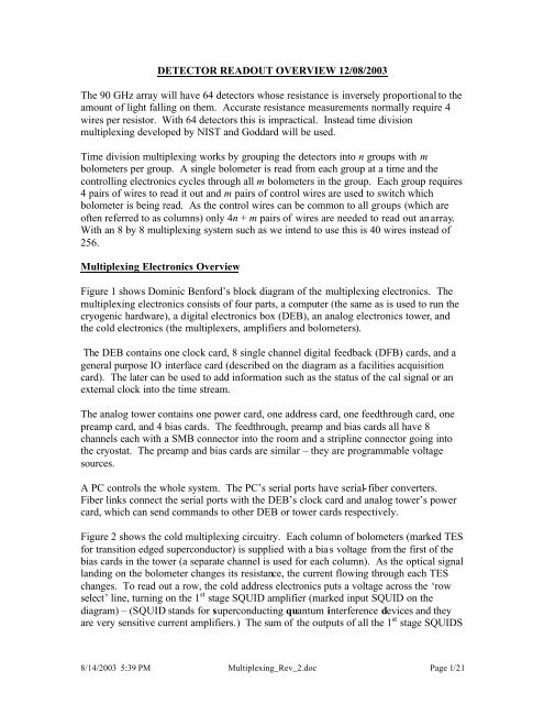
Figure 1 shows Dominic Benford’s block diagram of the multiplexing electronics. <strong>The</strong><br />
multiplexing electronics consists of four parts, a computer (the same as is used to run the<br />
cryogenic hardware), a digital electronics box (DEB), an analog electronics tower, and<br />
the cold electronics (the multiplexers, amplifiers and bolometers).<br />
<strong>The</strong> DEB contains one clock card, 8 single channel digital feedback (DFB) cards, and a<br />
general purpose IO interface card (described on the diagram as a facilities acquisition<br />
card). <strong>The</strong> later can be used to add information such as the status of the cal signal or an<br />
external clock into the time stream.<br />
<strong>The</strong> analog tower contains one power card, one address card, one feedthrough card, one<br />
preamp card, and 4 bias cards. <strong>The</strong> feedthrough, preamp and bias cards all have 8<br />
channels each with a SMB connector into the room and a stripline connector going into<br />
the cryostat. <strong>The</strong> preamp and bias cards are similar – they are programmable voltage<br />
sources.<br />
A PC controls the whole system. <strong>The</strong> PC’s serial ports have serial-fiber converters.<br />
Fiber links connect the serial ports with the DEB’s clock card and analog tower’s power<br />
card, which can send commands to other DEB or tower cards respectively.<br />
Figure 2 shows the cold multiplexing circuitry. Each column of bolometers (marked TES<br />
for transition edged superconductor) is supplied with a bias voltage from the first of the<br />
bias cards in the tower (a separate channel is used for each column). As the optical signal<br />
landing on the bolometer changes its resistance, the current flowing through each TES<br />
changes. To read out a row, the cold address electronics puts a voltage across the ‘row<br />
select’ line, turning on the 1 st stage SQUID amplifier (marked input SQUID on the<br />
diagram) – (SQUID stands for superconducting quantum interference devices and they<br />
are very sensitive current amplifiers.) <strong>The</strong> sum of the outputs of all the 1 st stage SQUIDS<br />
8/14/<strong>2003</strong> 5:39 PM Multiplexing_Rev_2.doc Page 1/21
in each column is fed into another 2 stages of SQUID amplifiers before passing out of the<br />
cryostat via the preamp card. <strong>The</strong> preamp card also provides biasing (power) for the 3 rd<br />
stage of amplification (which is often referred to as the series <strong>array</strong>). Biasing for the 2 nd<br />
stage of amplification is provided by the second of the bias cards. Each channel from the<br />
preamp card goes to a separate DFB card in the digital electronics box where the signal is<br />
digitized.<br />
Although SQUIDs are very sensitive their response is also periodic. To avoid problems<br />
associated with this the NIST/Goddard electronics uses a feedback system to keep the<br />
output from the preamplifier constant. Using a digital PI algorithm, the DFB cards output<br />
a voltage that gets feed back all the way to the input of the 1 st stage SQUID (via the<br />
feedthrough card) and cancel out any changes in the signal from the bolometer. <strong>The</strong><br />
output from the electronics to the computer (via fiber optic) is the size of this voltage. As<br />
the system multiplexes, the DFB cards have to change this feedback signal in sync with<br />
the switching of the ‘row select’ lines. <strong>The</strong> clock and address cards keep everything in<br />
sync.<br />
As the 2 nd and 3 rd stage SQUIDS also have periodic outputs it is important to set up the<br />
<strong>array</strong> correctly so that they are functioning on the most responsive parts of their curves.<br />
<strong>The</strong> region of the response curve they are operating at is adjusted by applying a voltage to<br />
the 2 nd and 3 rd stage feedback connections (see figure 2). <strong>The</strong>se voltages are provided by<br />
the third and fourth bias cards in the tower. To find the correct values, the DFB cards are<br />
used to apply a triangle wave to the 1 st stage circuits. <strong>The</strong> feedback/bias values that give<br />
the maximum signal can then be found. A method for carrying this out automatically is<br />
currently under investigation. (see below)<br />
<strong>The</strong> rest of this document describes each of the components of the detector read out<br />
system, version 2.1. On the GBT we expect to be using version 3.0 which is an update to<br />
the firmware running the DFB boards. Further details are given in the section on the<br />
DFB. All other components will stay the same and the methods for talking to the boards<br />
will not change. For more information on time division multiplexing, see Benford et al.<br />
Multiplexed Readout of Superconducting Bolometers. International Journal of Infrared<br />
and Millimeter Waves. 21:(<strong>12</strong>) 1<strong>90</strong>9-1916.<br />
<strong>The</strong> PC<br />
<strong>The</strong> heart of the system is a PC running Red Hat Linux version 7.3 with the bigphysarea<br />
patch and the kernel updated to version 2.4.20. <strong>The</strong>se patches are necessary to allow a<br />
custom input card to use large physical areas of memory. <strong>The</strong> PC controls the cryogenics<br />
system via a GPIB card (see cryogenics_system_overview_2 document). <strong>The</strong> PC also<br />
contains 3 serial ports which are used to control the multiplexing electronics, as well as a<br />
PCI Fiber DIO card to read the multiplexed data. <strong>The</strong> PCI Fiber card streams data from<br />
up to 16 fiber links (8 used, 8 unused), each one coming from a digital feedback card.<br />
Serial ports<br />
<strong>The</strong> PC contains three serial ports, COM0, COM2, and COM3:<br />
8/14/<strong>2003</strong> 5:39 PM Multiplexing_Rev_2.doc Page 2/21
COM0 connects to the digital electronics box’s clock card.<br />
COM2 connects to the analog electronics tower’s power card.<br />
COM3 connects to a relay box and is used for calibration purposes which are not relevant<br />
here.<br />
COM0 and COM2 use serial to fiber converters to transmit data over optical fiber in<br />
simplex mode.<br />
<strong>The</strong> Analog Towe r<br />
Addresses of cards in the analog tower are burned into the PROMs. Because of this,<br />
obtaining replacement cards is more difficult once each card in the system is assigned its<br />
permanent address. <strong>The</strong>refore, until we have a working setup we will not assign cards<br />
(with their permanent addresses) to specific functions.<br />
Data written over COM2 to the analog tower consists of a 9-bit address, 3-bit subaddress,<br />
and a 16-bit data value. <strong>The</strong>se 28 bits are packaged with 4 framing bits to produce 4<br />
bytes, which are sent in the following fashion:<br />
MSB<br />
LSB<br />
b 7 b 6 b 5 b 4 b 3 b 2 b 1 b 0<br />
0 d 6 d 5 d 4 d 3 d 2 d 1 d 0 Byte 1<br />
0 d 13 d <strong>12</strong> d 11 d 10 d 9 d 8 d 7 Byte 2<br />
0 a 1 a 0 sa 2 sa 1 sa 0 d 15 d 14 Byte 3<br />
1 a 8 a 7 a 6 a 5 a 4 a 3 a 2 Byte 4<br />
Where the 9 bit address is reperesented as:<br />
a 8 a 7 a 6 a 5 a 4 a 3 a 2 a 1 a 0<br />
<strong>The</strong> 3 bit subaddress value is represented as:<br />
sa 2 sa 1 sa 0<br />
And the 16 bit data value is represented as:<br />
d 15 d 14 d 13 d <strong>12</strong> d 11 d 10 d 9 d 8 d 7 d 6 d 5 d 4 d 3 d 2 d 1 d 0<br />
Within each byte, the LSB (least significant bit) is sent first. Within each packet, Byte 1<br />
is sent first.<br />
Note that the MSB (most significant bit) of each byte sent over the serial port is a framing<br />
bit, with a 1 indicating the last byte of a transfer. Also note that communication is one<br />
way; there is no way for the PC to check that valid data has been received.<br />
<strong>The</strong> exact meanings of address, subaddress, and value depend on the card being written<br />
to.<br />
1) DACs – bias and preamp cards<br />
8/14/<strong>2003</strong> 5:39 PM Multiplexing_Rev_2.doc Page 3/21
Each of the DAC (digital to analog converter) cards (bias and preamp cards) contain 8<br />
programmable voltage sources to properly biases various stages of amplification or<br />
provide the correct feedback voltage. In addition, the preamp card (which is connected to<br />
the 3rd SQUID stage) outputs an amplified version of its input to the SMB connectors,<br />
which gets routed to the DEB for sampling. <strong>The</strong> bias card’s SMB connectors function as<br />
additional inputs which can be added to the DAC output, or used to monitor the voltage<br />
at the DAC output.<br />
<strong>The</strong> meanings of the address, subaddress, and value fields are as follows:<br />
Address<br />
Subaddress<br />
Data<br />
9 bits for the destination card address<br />
Each DAC card has 8 channels indexed by these 3 bits<br />
A 16 bit DAC value corresponding to a voltage<br />
range of 0 (0x000) to 2.5 V (0xFFFF)<br />
2) Address card<br />
<strong>The</strong> meanings of the address, subaddress, and value fields are as follows:<br />
Address represents the destination card address<br />
Subaddress chooses one of several functions, which determines the meaning of data<br />
Subaddress (binary) Function Data High Bit Low Bit<br />
000 Program ILUT LUT_ADDRESS d15 d10<br />
PGM_DATA d8 d4<br />
001 Set Vref 14-bit DAC value d15 d2<br />
010 Set ILUT parameters ILUT_DELTA d15 d10<br />
ILUT_START d8 d3<br />
011 Start enable All 1s for on, 0s for off d15 d0<br />
100 Set NSTEP NSTEP d7 d0<br />
101 Enable address driver All 1s for on, 0s for off d15 d0<br />
<strong>The</strong> address card contains a look up table (LUT) of 64 entries (address 0 to 63). Each<br />
entry contains a 5 bit word. <strong>The</strong> values stored are unsigned decimals. <strong>The</strong> values, which<br />
can range from 0 to 31, represent rows of SQUIDs. Upon reset, the system’s LUT<br />
defaults to 0 through 31 for entries 0 through 31, and 0 for the remaining 32 entries. <strong>The</strong><br />
user can choose to create a new LUT if desired.<br />
<strong>The</strong> LUT determines which row of SQUIDs is accessed at any given time. <strong>The</strong> address<br />
card starts at ILUT_START, and progresses through the LUT, incrementing by<br />
ILUT_DELTA, addressing the row that has its number stored in the LUT. <strong>The</strong> card<br />
goes back to the start of the LUT after (NSTEP+1) rows have been addressed.<br />
“Addressing the row” means that the address card physically applies a voltage (Vref) to<br />
the bias line for that row.<br />
For the Penn Array we wish to address rows 0 through 7, so the default LUT is correct.<br />
<strong>The</strong> other parameters should be set as:<br />
ILUT_START = 0<br />
8/14/<strong>2003</strong> 5:39 PM Multiplexing_Rev_2.doc Page 4/21
ILUT_DELTA = 1<br />
NSTEP = 7<br />
<strong>The</strong> LUT can be changed using the PGM_DATA and LUT_ADDRESS fields. <strong>The</strong><br />
value stored in PGM_DATA is stored at the LUT address pointed to by<br />
LUT_ADDRESS. So, if one wanted to change LUT entry 5 (address 4) with the value<br />
25, one would program the card with the following data:<br />
LUT_ADDRESS = “00100”<br />
PGM_DATA = “11001”<br />
Summary of parameters on address card:<br />
• LUT_ADDRESS is a pointer to where in the LUT the data in PGM_DATA<br />
should be stored.<br />
• Vref is the bias voltage used to ‘turn on’ 1 of 32 SQUID rows.\<br />
• ILUT_DELTA is the amount by which the index is incremented.<br />
• ILUT_START is the address to start indexing at.<br />
• Start_enable enables/disables the Address Card to begin generating address data<br />
at its output.<br />
• NSTEP is the number of transitions to make before going back to ILUT_START<br />
(also NSTEP = #rows – 1)<br />
• Enable address driver allows the user to disable the Address Driver. It will not<br />
be used regularly.<br />
<strong>The</strong> following sequence of bytes should be written to the analog tower to properly<br />
configure the address card for the Penn Array.<br />
a8..a0 should be substitured with the address of the address card<br />
x = don’t care<br />
MSB<br />
LSB<br />
b 7 b 6 b 5 b 4 b 3 b 2 b 1 b 0<br />
0 0 0 0 0 x x x Byte 1 First 4 bytes set ILUT_DELTA<br />
0 0 0 0 1 x 0 0 Byte 2 and ILUT_START.<br />
0 a 1 a 0 0 1 0 0 0 Byte 3<br />
1 a 8 a 7 a 6 a 5 a 4 a 3 a 2 Byte 4<br />
0 0 0 0 0 1 1 1 Byte 5 Next 4 bytes set NSTEP = 7<br />
0 x x x x x x 0 Byte 6<br />
0 a 1 a 0 1 0 0 x x Byte 7<br />
1 a 8 a 7 a 6 a 5 a 4 a 3 a 2 Byte 8<br />
Vref must also be written, but this value has not yet been determined<br />
After that:<br />
0 1 1 1 1 1 1 1 Byte 13 Start_enable<br />
0 1 1 1 1 1 1 1 Byte 14<br />
0 a 1 a 0 0 1 1 1 1 Byte 15<br />
1 a 8 a 7 a 6 a 5 a 4 a 3 a 2 Byte 16<br />
8/14/<strong>2003</strong> 5:39 PM Multiplexing_Rev_2.doc Page 5/21
<strong>The</strong> Digital Electronics Box<br />
Each card in the DEB has an 8 bit DIP switch for setting the card address. <strong>The</strong> address<br />
assignments are shown below.<br />
Card Address<br />
Clock 0<br />
DFB 1 1<br />
DFB 2 2<br />
DFB 3 3<br />
DFB 4 4<br />
DFB 5 5<br />
DFB 6 6<br />
DFB 7 7<br />
DFB 8 8<br />
Data written over COM0 to the DEB consists of a 7-bit address, 3-bit register address,<br />
and a 25-bit data value. Each card has a unique 7-bit address, and each card may have up<br />
to 8 registers, which are indexed using the respective fields. <strong>The</strong> 25 bit data value is<br />
stored in the given register on the given card.<br />
<strong>The</strong>se 35 bits are packaged with 5 framing bits to produce 5 bytes, which are sent in the<br />
following fashion:<br />
MSB<br />
LSB<br />
b 7 b 6 b 5 b 4 b 3 b 2 b 1 b 0<br />
d 6 d 5 d 4 d 3 d 2 d 1 d 0 0 Byte 1<br />
d 13 d <strong>12</strong> d 11 d 10 d 9 d 8 d 7 0 Byte 2<br />
d 20 d 19 d 18 d 17 d 16 d 15 d 14 0 Byte 3<br />
r 2 r 1 r 0 d 24 d 23 d 22 d 21 0 Byte 4<br />
a 6 a 5 a 4 a 3 a 2 a 1 a 0 1 Byte 5<br />
Where the 7 bit address is reperesented as:<br />
a 6 a 5 a 4 a 3 a 2 a 1 a 0<br />
<strong>The</strong> 3 bit register address is represented as:<br />
r 2 r 1 r 0<br />
And the 25 bit data value is represented as:<br />
d 24 d 23 d 22 d 21 d 20 d 19 d 18 d 17 d 16 d 15 d 14 d 13 d <strong>12</strong> d 11 d 10 d 9 d 8 d 7 d 6 d 5 d 4 d 3 d 2 d 1 d 0<br />
Within each byte, the LSB is sent first, and within each packet, Byte 1 is sent first.<br />
Note that the LSB of each byte sent over the serial port is a framing bit, with a 1<br />
indicating the last byte of a transfer. This is in contrast to the analog tower<br />
communications protocol, which uses the MSB for framing. Also, note that<br />
communication is one way; there is no way for the PC to check that valid data has been<br />
received.<br />
8/14/<strong>2003</strong> 5:39 PM Multiplexing_Rev_2.doc Page 6/21
1) Clock card<br />
<strong>The</strong> time division multiplexing system uses 4 clock signals. CLK is the master clock<br />
signal, running at 50 MHz. LSYNC is essentially a row clock; it pulses after a full row of<br />
SQUIDs has been read, telling the address card to switch to the next row. FRM pulses<br />
once the last row has finished (a frame is one cycle through all the rows). ADR_CK runs<br />
at twice the rate of LSYNC and is used by the address cards.<br />
<strong>The</strong> clock card is responsible for CLK and FRM. <strong>The</strong> DFB cards make their own copy of<br />
LSYNC. <strong>The</strong> frequency of FRM is equal to (50 MHz / clock_divider).<br />
<strong>The</strong> clock card contains 2 25-bit registers, described in the table below.<br />
address field High Bit Low Bit<br />
1 stop 24 24<br />
start 23 23<br />
2 clock_divider 24 0<br />
Field names and definitions:<br />
• STOP and START bits are used at the very start of turning the system on to first<br />
make sure the card is started. If the card does not start correctly (as evidenced by<br />
the yellow light on the card not blinking), STOP must be sent, followed by<br />
START again. <strong>The</strong>re is no way to check from the system if it started correctly.<br />
We do not know yet if this will be a problem for us.<br />
• clock_divider determines the frequency of the FRM clock. This frequency is<br />
equal to 50 MHz divided by the number stored in clock_divider<br />
Other important info:<br />
• <strong>The</strong> 25 bits of Register 1 consists of only 2 meaningful bits.<br />
• <strong>The</strong>re is no register 0.<br />
2) Digital Feedback Card<br />
Each DFB card uses an ADC to sample the SA output. A proportional/integral (PI)<br />
control algorithm is implemented by digital electronics, and the output is converted back<br />
to an analog voltage through a DAC. <strong>The</strong> DAC output is connected to the bias line of the<br />
first stage of SQUIDs.<br />
<strong>The</strong> DFB cards are also responsible for sending all the multiplexed data to the PC for<br />
storage on hard disk. This is accomplished through direct fiber links to the PCI Fiber<br />
card.<br />
<strong>The</strong> DFB cards also contain a programmable triangle wave generator. When active, the<br />
DAC outputs a triangle wave to the SQUID feedback, which is used to observe the full<br />
8/14/<strong>2003</strong> 5:39 PM Multiplexing_Rev_2.doc Page 7/21
esponse of the SQUIDs to different feedback levels. By monitoring the output, the<br />
optimal feedback level can be determined. <strong>The</strong> cycles per step can be changed to<br />
determine the frequency of the wave, and the number of steps and step size to determine<br />
the height and resolution of the wave. <strong>The</strong> value of the wave changes at a frequency of<br />
(2*CyclesperStep*line rate), and it changes NumSteps times, giving the triangle wave<br />
itself a frequency of (2*CyclesperStep*line rate / (NumSteps+1)). For example, if the<br />
line rate is 1 MHz, CyclesperStep is 1, NumSteps is 3, and StepSize is 1, then you will<br />
have a 500 kHz triangle wave ranging between 8 and 0 in steps of 1.<br />
<strong>The</strong> digital feedback card contains 8 registers. <strong>The</strong> register structure is shown below.<br />
address size addrsize field name High Bit Low Bit Arrayed Signed<br />
0 25 3 2*lsync_clock_divider d24 d0 Yes No<br />
1 25 3 ADC _offset / lockpoint d15 d0 Yes No<br />
2 25 3 Triangle Disable d16 d16 Yes No<br />
DAC_offset d15 d0 Yes No<br />
3 25 3 FB on/off d24 d24 Yes No<br />
pval d19 d10 Yes Yes<br />
ival d9 d0 Yes Yes<br />
4 25 3 triangle cycles/step d23 d20 No No<br />
triangle # of steps d19 d16 No No<br />
tri_step_size d15 d0 No No<br />
5 25 3 START_EN d7 d7 No No<br />
Row number d6 d1 No No<br />
send_mode d0 d0 No No<br />
6 25 3 #samples d19 d0 No No<br />
7 25 3 global_reset d24 d24 No No<br />
NSTEP d14 d8 No No<br />
settling time d7 d0 No No<br />
Field names and definitions:<br />
• 2*LSYNC_CLOCK_Divider will be used for a user-programmable clock divider<br />
to generate LSYNC and ADR_CK pulses. As mentioned earlier, the DFB cards<br />
generate their own LSYNC clocks and its frequency is (50 MHz /<br />
lsync_clock_divider). ADR_CK runs at twice the rate of LSYNC and is used by<br />
the address cards.<br />
• ADC offset/lockpoint – the DFB card attempts to lock the output at the ADC<br />
lockpoint.<br />
• Triangle Disable turns off the triangle wave generator<br />
• DAC offset – offset applied to DFB card’s DAC (for both feedback and triangle<br />
wave purposes)<br />
• FB on/off – single bit indicating whether or not the feedback algorithm is enabled<br />
• Pval – proportional gain for DFB PI control algorithm<br />
• Ival – integral gain for DFB PI control algorithm<br />
• Triangle cycles per step – Value of triangle wave will change at a frequency of<br />
2*CyclesperStep * line rate<br />
8/14/<strong>2003</strong> 5:39 PM Multiplexing_Rev_2.doc Page 8/21
• triangle # of steps – Number of times to count up values of the triangle wave.<br />
• triangle step size – Size of step being incremented<br />
• START_EN – enables addressing by address card<br />
• Row number determines which row the <strong>array</strong>ed registers will apply to. See below<br />
for more info on <strong>array</strong>ed registers.<br />
• send_mode – chooses between 2 different modes for streaming data to PCI card<br />
(see section on PCI Data Streaming for more information)<br />
o Mode 0: D2A[13..0], OVERFLOW, FRAME, ERROR[15..0]<br />
o Mode 1: ERROR[15..0], FRAME, OVERFLOW, D2A[13..0]<br />
• # of samples – number of samples over which to average when calculating error<br />
signal – higher number means slower, but more accurate, response<br />
• Global reset – starts the muxing over at the first row<br />
• NSTEP – number of row transitions per frame, i.e. the number of rows being<br />
MUXed = NSTEP+1<br />
• Settling_time – number of clock cycles to wait, and let input settle, before<br />
sampling input to calculate feedback<br />
Important items:<br />
• pval and ival are signed numbers, in 10-bit 2’s complement notation<br />
• Registers 0-3 are considered “Arrayed registers”. Each DFB card controls a<br />
column, and thus must have room for different DAC offsets, P/I values, etc., for<br />
each of the rows it accesses. To write an <strong>array</strong>ed value to a specific row, first set<br />
the row number (register 5) and then write any necessary <strong>array</strong>ed registers. On<br />
the Penn Array, each DFB card will carry 8 different values for each of the fields<br />
in registers 0-3.<br />
• Registers 4-7 are considered “Non-<strong>array</strong>ed registers” in that each DFB card has<br />
only one set of values for these.<br />
As of 14/8/<strong>2003</strong> we expect to be updating the firmware in these cards. Changes include<br />
• <strong>The</strong> PI feedback algorithm – a different equation & parameters will be used.<br />
• Additional choices of waveform output (sine, sawtooth…..)<br />
• Including clock pulses/frame numbers in the output data.<br />
• Other additions to the output data.<br />
<strong>The</strong> method of communication will be the same but some of the values to be passed will<br />
have to change.<br />
3) Interface Card<br />
<strong>The</strong> interface card interfaces the DEB to other systems. It provides the address card with<br />
a 2*LSYNC clock, as well as the FRM sync signal. It also has 4 general purpose analog<br />
inputs and 4 general purpose digital inputs. <strong>The</strong>se inputs would come from an external<br />
system, on a separate ground plane. <strong>The</strong> data on these lines is synchronized with the<br />
Mark III data stream and sent into the PCI card.<br />
8/14/<strong>2003</strong> 5:39 PM Multiplexing_Rev_2.doc Page 9/21
Register Field High Bit Low Bit<br />
1 2*LSYNC_CLOCK divider 24 0<br />
2 Enable ADC #1 24 24<br />
ADC #1 Ch. 0 conversion time 23 17<br />
ADC #1 Ch. 1 conversion time 16 10<br />
3 Enable ADC #2 24 24<br />
ADC #2 Ch. 0 conversion time 23 17<br />
ADC #2 Ch. 1 conversion time 16 10<br />
4 Status Dump enable 24 24<br />
<strong>The</strong> ADC used in the Interface Card is the Analog Devices AD7732. <strong>The</strong><br />
firmware will automatically configure it for a ±5V input range, No Chopping, and 24-bit<br />
Continuous Conversion Mode. <strong>The</strong>se parameters are not user-configurable at this time.<br />
Sampling Rate for all four channels will be user-configurable. To calculate the sampling<br />
rate, use the following formula, where FW is the 7-bit Conversion Time parameter:<br />
(((FW * 64) + 207) / 6.144) MHz<br />
<strong>The</strong> PCI Data Stream<br />
DFB Cards<br />
<strong>The</strong>re are 2 possible modes for streaming from the DFB cards, and they produce slightly<br />
different data structures (they only differ in bit order).<br />
• Mode 0: D2A[13..0], OVERFLOW, FRAME, ERROR[15..0]<br />
• Mode 1: ERROR[15..0], FRAME, OVERFLOW, D2A[13..0]<br />
<strong>The</strong> data is arranged from MSB to LSB, and is left-shifted out of the fiber link, so that the<br />
MSB is sent first. Exactly how the PCI card processes this is unclear right now. We<br />
know that FRAME becomes the first bit of the third byte written to the file, but the mode<br />
(0 or 1) for that situation was unknown, so either Mode 0 is written to file from right to<br />
left or Mode 1 is written LSB first.<br />
Each data packet is 32 bits:<br />
• <strong>The</strong> 14 bit D2A value represents the DAC output of the DFB card at that instant<br />
• <strong>The</strong> 16 bit ERROR signal is the difference between the ADC lockpoint and the<br />
ADC sampled input (not an error code in the sense of a mistake, but in the sense<br />
of a difference between the desired value and the actual value).<br />
• OVERFLOW is a single bit indicating whether or not the card overflowed (i.e.,<br />
parameters should be changed or data disregarded)<br />
• FRAME is a single bit indicating the start of a new frame of data<br />
Interface Card<br />
<strong>The</strong> interface card sends its digital and analog inputs to the PCI card. <strong>The</strong> bit stream<br />
consists of 2 32-bit words.<br />
8/14/<strong>2003</strong> 5:39 PM Multiplexing_Rev_2.doc Page 10/21
• Word 0: 0, FRAME, 0, 0, DIG[3..0], ADC0[23..0]<br />
• Word 1: 0, FRAME, 0, 1, DIG[3..0], ADC1[23..0]<br />
<strong>The</strong> data is arranged from MSB to LSB, and is left-shifted out of the fiber link, so that the<br />
MSB is sent first. Exactly how the PCI card processes this is unclear right now.<br />
<strong>The</strong> 64 bits are relay the following information:<br />
• FRAME is a single bit indicating that frame_sync is high<br />
• DIG[3..0] are the 4 general purpose digital inputs.<br />
• <strong>The</strong> 24 bit ADCx signals are the general purpose analog inputs.<br />
SQUID Biasing Algorithm<br />
We have been told there may be an algorithm in development that will automatically bias<br />
all of the SQUIDs properly. Until then, properly biasing the SQUIDs is a long procedure<br />
that must be repeated for each SQUID, and is not something the user should have to do<br />
each time.<br />
Currently, the procedure, in the context of the python GUIs, is as follows. Note that the<br />
following procedures work with an older version of the firmware and will not work in<br />
exactly the same way with our hardware, but this is a general idea of the necessary steps.<br />
Turning on system – muxclock.py:<br />
In the ‘sync’ tab: Issue stop command, then start command. Yellow light should blink<br />
(not go all the way up and remain on).<br />
Basic procedure for properly biasing a SQUID – use dfbmuxgui.py (for DEB<br />
communication) and SQUID2.py (for analog biases):<br />
1. Turn a triangle wave generator on and send this to the flux feedback (FB) line for<br />
the desired SQUID.<br />
2. View series <strong>array</strong> (SA) output on scope – looks nearly sinusoidal.<br />
3. Change DAC offset level to maximize amplitude without clipping. Princeton<br />
reports 40000 to be approximately correct.<br />
4. Measure DC value of point on curve with greatest slope – pretty much the center<br />
of the sinusoidish output.<br />
5. Remove the triangle wave and set the voltage on the bias card connected to the<br />
feedbackline so that the DC out is at approximately the same point as the center<br />
(biased at steepest point of curve) – this biases the SQUID correctly.<br />
<strong>The</strong>re are three stages of SQUIDs – the 1 st stage, 2 nd stage, and SA. To bias a full set of 3<br />
SQUIDs the SA should be done first, followed by the 2 nd stage and finally the 1 st stage.<br />
At this point, the DFB cards must be used to lock the feedback – use<br />
rack_addrboard.py<br />
1. Select address<br />
2. Width = 60 (we have no idea what that means, but NIST said so)<br />
8/14/<strong>2003</strong> 5:39 PM Multiplexing_Rev_2.doc Page 11/21
3. ADC high and ADC low should be approximately 14,200 – when ADC low is<br />
set low, the output gets very noisy<br />
4. On scope, we should see triangle wave and that vaguely sinusoidal shape<br />
again from the SA.<br />
5. We want to lock the feedback to the steepest point of the curve. <strong>The</strong>re are<br />
four controls to adjust: DAC offset, ADC offset, P, and I<br />
i. DAC offset should be changed first. It ranges from 0 to 16,383. Adjust<br />
until the DAC offset is at the center (steepest part) of the curve like in<br />
previous steps.<br />
ii. Next find ADC offset. This is calculated by finding voltage at center of<br />
curve (where we biased using the DAC offset), then multiply by (2 <strong>12</strong> *<br />
number of samples per detector (default to 16)) = (4,096 *<br />
samples/detector)<br />
iii. Next choose P and I values (proportional and integral values for PI<br />
controller). Princeton uses 50 and 50 as defaults. <strong>The</strong>n, attempt to lock<br />
channels (click lock, then send register).<br />
iv. If overflow light (top light on address card – can also be read in PCI data<br />
stream), lower P and I values (10 and 10 often work).<br />
v. Try lock and send again. If more trouble, increase settling time.<br />
Stream data to PCI card – pci_mux_control.py<br />
1. Fill in appropriate fields – channel #s, # of buffers, delay, etc.<br />
2. Click ‘save’ to stream data to disk<br />
PCI Fiber DIO Board Device Driver<br />
All information in this section has been obtained via reverse engineering the driver<br />
software, and has not been confirmed by anyone involved in the design of the board or<br />
driver.<br />
NIST has provided a driver for the PCI Fiber DIO board. <strong>The</strong> driver is written in C and is<br />
available as a C header file (aa.c) or a Python module (AA).<br />
Opening communication with PCI board<br />
<strong>The</strong> open() function is used to obtain a file handler for the PCI board. <strong>The</strong> “file” to open<br />
is “/dev/ab0”, and should be opened with “rwb” (read/write binary) permissions.<br />
Driver capabilities<br />
<strong>The</strong> driver contains implementations of the following standard functions:<br />
• open<br />
• poll<br />
• ioctl<br />
• release<br />
• mmap<br />
• fasync<br />
8/14/<strong>2003</strong> 5:39 PM Multiplexing_Rev_2.doc Page <strong>12</strong>/21
Of these, the only one requiring further explanation is ioctl, since the rest are standard.<br />
ioctl functions provided by driver<br />
<strong>The</strong> ioctl function is actually an interface to several other, device-specific functions. All<br />
the ioctl functions used by the NIST software are listed below, along with their meanings.<br />
Important: Some of these functions accept arguments. For all functions that require<br />
arguments, except ABIOCONFIGURE and ABIOSTART, the meaning of the argument is<br />
unclear, but the programs we have always pass 0 to the functions.<br />
• ABIOGA2PBUFFER – returns the address of the start of the buffer – accepts<br />
argument<br />
• ABIOGBUFFERSIZE – returns the size of the buffer (in kB) – accepts<br />
argument<br />
• ABIORESET – resets board and counter in the driver<br />
• ABIOCONFIGURE – writes a configuration word, passed as an argument, to<br />
the board – there is not much info on structure of configuration word – see<br />
below for more info<br />
• ABIOSTART – begins the DMA (Direct Memory Access) transfer from the<br />
board – the argument passed is some form of configuration word<br />
• ABIOSTOP – stops DMA transfer<br />
• ABIOGMWTC – returns the number of buffers left in the transfer –accepts<br />
argument<br />
• ABIOGBUFFNUMBER – returns the current buffer number – accepts<br />
argument<br />
• ABIOGCOUNTER – returns the current counter value – accepts argument<br />
<strong>The</strong> following ioctl functions exist in the driver but are not used in any of the sample<br />
software we have. Where possible, their purpose is noted. Any arguments are noted in<br />
the names.<br />
• ABIORESETADDON – resets the add-on – we don’t know what the “add-on”<br />
refers too, though<br />
• ABIOSETLATENCY(arg) – sets the PCI latency timer to the value of arg,<br />
where 0x20 ≤ arg ≤ 0xF8<br />
• ABIOSETNUMBUFFERS(arg) – sets the number of write buffers to arg<br />
• ABIOSETBUFFERSIZE(arg) – sets the size of the buffers to arg<br />
• ABIOGMCSR(arg) – prints the Bus Master Control Register information to<br />
the kernel log file<br />
• ABIOGINTCSR(arg) – prints the Interrupt Control Service Register<br />
information to the kernel log file<br />
• ABIOGINFOADDR(arg) – unknown<br />
• ABIOGP2ABUFFER(arg) – get some value from PCI card called<br />
pd_phys_read – function is unknown<br />
• ABIOGMRTC(arg) – ABIOGMWTC returns the number of buffers left to<br />
write; perhaps this returns the number left to read<br />
8/14/<strong>2003</strong> 5:39 PM Multiplexing_Rev_2.doc Page 13/21
• ABIOGNUMBUFFERS(arg) – returns the number of buffers in the transfer,<br />
in total<br />
• ABIOGCPUTIME(arg) – unknown<br />
ABIOCONFIGURE/ABIOSTART Configuration words<br />
No information is available on the precise meaning of most of the bits in the<br />
configuration words, written using ABIOCONFIGURE. However, the meaning of<br />
several complete words has been determined in context. Each configuration word is 4<br />
bytes long, and the known ones are shown below in hex, along with meanings.<br />
0x80000000 – clear FIFOs – use before stopping card<br />
(0x20000000 + channel_mask) – see next line<br />
(0x40000000 + channel_mask) – these 2 commands, used consecutively, “setup the<br />
streaming” for a given channel – the channel mask is constructed by assigning each of<br />
the 16 lowest bits in the word to represent a channel on the PCI card. For example, if<br />
bits 0, 1, and 3 are set, then the PCI card will read data from Channels 0, 1, and 3.<br />
0x80000000 + (delay * 0x10) – call immediately before issuing start command (with<br />
ABIOSTART) – the delay may range from 0 to 9 (default is 8)<br />
Note that the last 3 words above are used by ABIOSTART in one of the sample<br />
programs, the one showing how to stream from multiple channels. <strong>The</strong>re is a remote<br />
possibility that this is a mistake and they should be passed to ABIOCONFIGURE.<br />
ABIOSTART accepts one additional word:<br />
0x80000001 + (delay * 0x10) – tells PCI board to actually begin the data streaming<br />
Using ioctl<br />
ioctl is available in C, Python, and probably many other languages.<br />
ioctl in C:<br />
Header files needed:<br />
#include <br />
#include <br />
Function prototype:<br />
int ioctl(int fildes, int request, arg);<br />
fildes here is the file descriptor to the PCI board<br />
request is the name of the ioctl command, taken from the previous list<br />
arg is the optional argument that some of these functions require.<br />
8/14/<strong>2003</strong> 5:39 PM Multiplexing_Rev_2.doc Page 14/21
If an invalid request or argument are passed to ioctl, (-EINVAL) is returned. If the<br />
particular command is supposed to return something, like ABIOGBUFFERSIZE (gets<br />
the buffer size), then that value is returned.<br />
For example<br />
/* assume fd is the file handler for the PCI card */<br />
ioctl(fd, ABIOSTOP) /* stops card */<br />
bufsize = ioctl(fd, ABIOGBUFFERSIZE, 0); /* 0 is passed as an argument */<br />
Calling ioctl in Python<br />
Modules needed:<br />
import fcntl<br />
In Python, ioctl is a member of the fcntl class. Actual file descriptors may be<br />
obtained from Python’s higher level descriptors using the fileno() member function.<br />
Arguments to ioctl functions must be packed into a Python structure as an unsigned<br />
integer, which exposes the raw bit format of the data. Returned data must similarly<br />
be unpacked.<br />
For example:<br />
# assume fd is the file handler for the PCI card – to stop the card, use the following<br />
line<br />
fcntl.ioctl(fd.fileno(), AA.ABIOSTOP)<br />
# using an ioctl that requires an argument is more complicated:<br />
# First, the argument (0 in this case) must be packed into a structure in bit form<br />
arg = struct.pack(“L”, 0);<br />
# Next, call the actual ioctl – note that it is from the AA module, and must be<br />
# accessed as such (with AA. in front of it)<br />
msg = fcntl.ioctl(fd.fileno(), AA.ABIOGBUFFERSIZE, arg);<br />
# Finally the return value must be unpacked<br />
data = struct.unpack(“L”, msg);<br />
buffer_size = data[0];<br />
Other functions necessary for using driver:<br />
mmap – creates a memory map which allows us to read from an area of memory as if it<br />
were a file.<br />
mmap in C:<br />
#include <br />
void *mmap(void *addr, size_t length, int prot, int flags, int fildes, off_t offset);<br />
mmap in Python:<br />
import mmap<br />
mmap.mmap(fildes, length, flags, protection);<br />
<strong>The</strong> only important distinction between these two is the presence of the *addr<br />
argument in C. I do not know how this should be handled. Also, in Python, flags<br />
8/14/<strong>2003</strong> 5:39 PM Multiplexing_Rev_2.doc Page 15/21
and protection, along with the mmap function itself are all defined as members of<br />
the mmap class.<br />
signal – links a specific signal (interrupt) with an interrupt handler function.<br />
signal in C:<br />
#include <br />
void (*signal (int sig, void (*disp)(int)))(int);<br />
signal in Python:<br />
import signal<br />
signal.signal(sig, handler)<br />
Note that in Python signal is a member of the signal class. <strong>The</strong> PCI Fiber board<br />
asserts the SIGIO signal (signal.SIGIO in Python).<br />
fcntl – fcntl is very similar to ioctl, but contains built-in functions. It is needed to finish<br />
configuring the interrupt handler, after the signal() call.<br />
fcntl in C:<br />
#include <br />
#include <br />
#include <br />
int fcntl(int fildes, int cmd, /* arg */ ...);<br />
fcntl in Python:<br />
import fcntl, FCNTL<br />
fcntl.fcntl(fildes, cmd, arg);<br />
Like ioctl, fcntl calls the “cmd” specified on the file descriptor. Relevant fnctl<br />
commands are F_SETOWN, F_GETFL, F_SETFL. fcntl’s return value depends<br />
on the command being passed.<br />
F_SETOWN sets the ownership of a process. We use it, immediately after<br />
configuring signal() with its handler, to finish the configuration.<br />
In C:<br />
fcntl(fd, F_SETOWN, getpid()); // getpid() is a function that gets the process ID<br />
In Python:<br />
fcntl.fcntl(fd.fileno(), FCNTL.F_SETOWN, os.getpid())<br />
F_GETFL and F_SETFL get and set, respectively, the flags associated with a file<br />
descriptor.<br />
In C:<br />
flags = fcntl(fd, F_GETFL);<br />
fcntl(fd, F_SETFL, flags | FASYNC); // set flag for asynchronous notification<br />
In Python:<br />
flags = fcntl.fcntl(fd.fileno(), FCNTL.F_GETFL);<br />
fcntl(fd.fileno(), FCNTL.F_SETFL, flags | FCNTL.FASYNC);<br />
8/14/<strong>2003</strong> 5:39 PM Multiplexing_Rev_2.doc Page 16/21
Reading Data<br />
All information in this section has been obtained via reverse engineering the NIST<br />
Python software, and has not been confirmed by anyone involved in the design of the<br />
board or driver.<br />
<strong>The</strong> PCI Fiber DIO card reads data from the DFB cards via direct fiber links. Each<br />
channel on the PCI card contains a memory buffer that, when full, causes the card to<br />
issue a SIGIO interrupt. Software must initialize the card for data streaming, listen for<br />
interrupts, read the data from the card and write it to a disk file, and finally stop the<br />
streaming.<br />
General Outline<br />
1) Open a PCI device handler, memory map, and data storage file<br />
2) Prepare an interrupt handler for when the PCI card buffer is full<br />
3) Reset the board<br />
4) Setup the channels for streaming<br />
5) Start the DMA to read from the PCI card<br />
6) When buffer is full, interrupt handler is called, which reads from the right memory<br />
map location, and write this data to the data file, and repeats DMA as necessary until<br />
streaming is complete.<br />
7) When finished taking data, clear FIFOs on card and stop streaming<br />
Detailed Steps – Essentially a line by line explanation of the Python streaming script<br />
– all specific functions referred to in this section are from Python, though in most<br />
instances there is a near exact correspondence with C functions. See above for more<br />
information on necessary functions. In most cases, C functions can be obtained<br />
simply be removing the class membership operation in functions (instead of<br />
fcntl.ioctl() just use ioctl(), instead of mmap.MAP_SHARED just use<br />
MAP_SHARED).<br />
1. Open a PCI device handler, memory map, and data storage file<br />
• <strong>The</strong> PCI device handler is found at “/dev/ab0”. It should be opened with mode<br />
“rwb” (read/write binary).<br />
• <strong>The</strong> memory map file descriptor (memfd) is located at “/dev/mem”. It should be<br />
opened as a file, with os.O_RDWR as the mode (read/write).<br />
• Create a memory map (mem) to memfd using the mmap command.<br />
• Memory map size = buffer_addr + total_size.<br />
• buffer_addr is obtained from the ABIOGA2PBUFFER ioctl<br />
• buffer_size in kB is obtained from the ABIOGBUFFERSIZE ioctl<br />
• total_size = buffer_size in bytes * 2 /* purpose is somewhat<br />
unclear – we suspect that instead of 2, this number should = # of columns<br />
being MUXed*/<br />
• Flags = mmap.MAP_SHARED /* this allows other things to access the<br />
mapped memory */<br />
• Protection = mmap.PROT_READ | mmap.PROT_WRITE. /* read/write<br />
mode */<br />
8/14/<strong>2003</strong> 5:39 PM Multiplexing_Rev_2.doc Page 17/21
• Create a file handler for the data file. Name and location may vary. Open in<br />
“wb” mode (write binary)<br />
2. Prepare interrupt handler<br />
• When the PCI board’s buffers are full, it asserts a SIGIO signal, so before that we<br />
must link the SIGIO signal to our interrupt handler using the signal() function<br />
• Set ownership on these interrupts using the F_SETOWN command to the fcntl()<br />
function. <strong>The</strong> first argument should be the file descriptor for the PCI board. <strong>The</strong><br />
last argument should be os.getpid() to get the proper process ID.<br />
• Set necessary FCNTL flags for the PCI file descriptor.<br />
• Get current flags using the FCNTL.F_GETFL argument passed to fcntl()<br />
• Set the flags to the current flags ORed with FCNTL.FASYNC to allow<br />
asynchronous notification.<br />
3. Reset the board<br />
• Call the ABIORESET ioctl function.<br />
4. Setup the channels for streaming<br />
• Build the channel mask<br />
• <strong>The</strong> channel mask is a bit mask with a 1 for each channel to include in the<br />
DMA, and a 0 for each channel not to.<br />
• Example 1 – to stream just to channels 0 and 1, channelmask=0000 0011 b<br />
• Example 2 – to stream channels 0-7, channelmask=0x00ff<br />
• Call ABIOSTART ioctl with 0x20000000+channelmask as argument /* there is a<br />
remote possibility that this should actually be ABIOCONFIGURE */<br />
• Call ABIOSTART ioctl with 0x40000000+channelmask as argument /* there is a<br />
remote possibility that this should actually be ABIOCONFIGURE */<br />
5. Start the DMA to read from the PCI card<br />
• Calculate delayBits = “Delay” value (range 0-9, default 8) * 0x10<br />
• Call ABIOSTART ioctl with 0x80000001+delayBits<br />
6. Interrupt handler takes over<br />
• Get the buffer number using the ABIOGBUFFNUMBER ioctl. Pass 0 as its<br />
argument.<br />
• Position the memory map pointer at the right place.<br />
• If buffer number = 1, position memory map at buffer_addr (using seek()<br />
function)<br />
• Else, position memory map at buffer_addr + buffer_size (the required offset)<br />
• Read a chunk of data of size buffer_size from the memory map using read()<br />
• Write this data to the disk data file.<br />
• If first_buffer=TRUE (which it is initialized to):<br />
• Find “frame offset” by proceeding through the first set of streamed data<br />
and examining the frame bit (see data stream section for more info).<br />
“Frame offset” = index of the packet containing a set frame bit (e.g., if the<br />
3 rd packet of streamed data contains a set frame bit, frame offset = 3).<br />
Note that the first two packets should be skipped since “the first few<br />
words are sometimes funny”.<br />
• Set first_buffer=FALSE<br />
• Write data to disk file at offset<br />
8/14/<strong>2003</strong> 5:39 PM Multiplexing_Rev_2.doc Page 18/21
• Python command used is data_fd.write(buffer(msg, self.offset)) – the<br />
buffer() function seems to convert the data into a set of chunks of<br />
address and data, with the offset added to the address – this was the<br />
only line of Python code that I could not decipher, and I felt it better to<br />
include the original code than to make a guess and possibly lose<br />
information<br />
• buffer_written = 1<br />
• Else if buffer_written != num_buffers<br />
• Write data to disk file – no offset needed since the file pointer is in the<br />
right place<br />
• Increment buffer_written<br />
• Else<br />
• Write data to disk file using an offset – Python command is<br />
data_fd.write(buffer(msg,0,self.offset)) – the meaning of this 0 is unclear<br />
• Stop streaming (go to step 7)<br />
7. Stop streaming<br />
• Clear FIFOs using ABIOCONFIGURE ioctl. Pass 0x80000000 as the argument<br />
• Stop card using ABIOSTOP ioctl.<br />
Existing Software for SQUID biasing, multiplexing, and feedback<br />
NIST has provided us with many Python scripts that control the analog tower, digital box,<br />
and can stream data from the detectors to the hard disk. <strong>The</strong> capabilities of each are<br />
described below.<br />
AA.py – PCI card driver module<br />
addr_board_dfb.py – programs the address card in the digital box – should not be run<br />
directly, but rather imported as a module for rack_addrboard.py – note that we will be<br />
using a newer address card in the analog tower, which makes the functioning of this<br />
script questionable<br />
cardclass.py – programs the “baseline” card (from an older version of the digital box),<br />
which we do not have or need<br />
clockcard.py – sets up the clock card in the digital box – muxclock.py seems to be a<br />
more complete version<br />
dfbmuxgui.py – programs the digital feedback cards in the digital box<br />
dfbmuxgui2.py – same as dfbmuxgui.py, with the added feature of a virtual oscilloscope<br />
that allows the user to click on the scope and automatically tune the SQUIDs to a<br />
given point<br />
8/14/<strong>2003</strong> 5:39 PM Multiplexing_Rev_2.doc Page 19/21
muxclock.py – sets up the clock card in the digital box – more complete than<br />
clockcard.py<br />
params.py – contains a few variable definitions which initialize some global variables<br />
for data streaming programs<br />
pci_mux_control.py – controls data streaming from up to 16 channels over the PCI fiber<br />
card, writing the information to disk<br />
pci_writex_mux.py – reads a single buffer full of data from a single channel of the PCI<br />
fiber card, writing the information to disk<br />
pci_writex_mux_multiple.py – reads many buffers full of data from a single channel of<br />
the PCI fiber card, writing the information to disk<br />
pyserial.py – defines some functions used to transmit data over the serial port – imported<br />
as a module by squid2.py<br />
rack_addrboard.py – configures address board in digital box – like addr_board_dfb.py,<br />
might not be useful for us since we have a different version of the address card – will<br />
have to be tested once the hardware is functioning<br />
rack_baseline_mux.py – configures “baseline” card – unnecessary for us<br />
squid2.py – communicates with analog tower, setting bias voltages<br />
Nomenclature<br />
ADC – Analog to Digital Converter<br />
CLK – Master Clock<br />
DAC – Digital to Analog Converter<br />
DEB – Digital Electronics Box<br />
DFB – Digital FeedBack<br />
DIO – Digital Input/Output<br />
DMA – Direct Memory Access<br />
FIFO – First In / First Out<br />
FRM – Frame Clock<br />
LSB – Least Significant Bit<br />
LSYNC – Line Synchronization Clock<br />
LUT – Look-Up Table<br />
MSB – Most Significant Bit<br />
MUX – MUltipleX<br />
PCI – Peripheral Control Interface<br />
PI – Proportional + Integral control<br />
PROM – Programmable Read-Only Memory<br />
SA – Series Array<br />
8/14/<strong>2003</strong> 5:39 PM Multiplexing_Rev_2.doc Page 20/21
SQUID – Superconducting QUantum Interference Device<br />
Notation<br />
0110 b – the number 0110 is in binary<br />
0x3F – the number 3F is in hexadecimal<br />
8/14/<strong>2003</strong> 5:39 PM Multiplexing_Rev_2.doc Page 21/21
Penn/GBT: 8x8 Array Electronics Block Diagram<br />
Computer Digital Electronics Analog Electronics<br />
User Interface<br />
2x Serial Out<br />
(fiber)<br />
IRC Software<br />
Fiber<br />
DIO<br />
(10 in)<br />
Archive<br />
Clock Card<br />
Digital Feedback<br />
Digital Feedback<br />
Digital Feedback<br />
Digital Feedback<br />
Digital Feedback<br />
Digital Feedback<br />
Digital Feedback<br />
Digital Feedback<br />
Facilities Acq<br />
Power Regulation<br />
Power Supply<br />
(grounded to dewar)<br />
flex-conections<br />
Nanonics-51<br />
terminators<br />
Power Card<br />
Address Card<br />
3rd Out A<br />
3rd FB A<br />
2nd Bias A<br />
1st FB A<br />
2nd FB A<br />
Detector Bias A<br />
flex-conections<br />
terminators<br />
input cable<br />
24 pairs<br />
Power Supply<br />
(grounded to dewar)<br />
Draft - Revision 1<br />
Nanonics-51<br />
Legend<br />
Oct-SA<br />
Housing<br />
8x8 GBT Package<br />
For muxing, only 8 addressed (16 wires) needed.<br />
8 pair 50Ω Flexline<br />
SMB Coax<br />
PreAmp<br />
Bias DAC<br />
Bias DAC<br />
Passthru<br />
Bias DAC<br />
Bias DAC<br />
Cryostat<br />
flex-conections<br />
Nanonics-65<br />
32-Address<br />
Driver<br />
(DeMux)<br />
(only 8 used)<br />
address cable<br />
32 pairs<br />
Single Fiber Optic<br />
Power cabling<br />
Woven NbTi/CuNi TekData cable<br />
Woven Cu TekData cable<br />
output cable<br />
8 pairs<br />
Nanonics-25