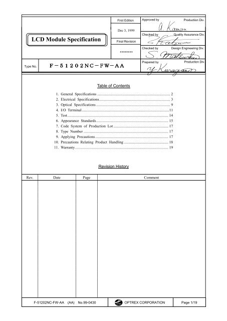
LCD Module Specification - Datasheets
LCD Module Specification - Datasheets
LCD Module Specification - Datasheets

You also want an ePaper? Increase the reach of your titles
YUMPU automatically turns print PDFs into web optimized ePapers that Google loves.
First Edition<br />
Approved by<br />
Production Div.<br />
<strong>LCD</strong> <strong>Module</strong> <strong>Specification</strong><br />
Dec 3, 1999<br />
Final Revision<br />
Checked by<br />
Quality Assurance Div.<br />
********<br />
Checked by<br />
Design Engineering Div.<br />
Type No.<br />
F-51202NC-FW-AA<br />
Prepared by<br />
Production Div.<br />
Table of Contents<br />
1. General <strong>Specification</strong>s ............................................................................ 2<br />
2. Electrical <strong>Specification</strong>s.......................................................................... 3<br />
3. Optical <strong>Specification</strong>s ............................................................................. 9<br />
4. I/O Terminal...........................................................................................11<br />
5. Test......................................................................................................... 14<br />
6. Appearance Standards........................................................................... 15<br />
7. Code System of Production Lot ......................................................... 17<br />
8. Type Number ........................................................................................ 17<br />
9. Applying Precautions............................................................................ 17<br />
10. Precautions Relating Product Handling .............................................. 18<br />
11. Warranty................................................................................................. 19<br />
Revision History<br />
Rev. Date Page Comment<br />
F-51202NC-FW-AA (AA) No.99-0430 OPTREX CORPORATION Page 1/19<br />
OPTREX
1.General <strong>Specification</strong>s<br />
Operating Temp. : min. 0℃ ~ max. 50℃<br />
Storage Temp. : min. -20℃ ~ max. 70℃<br />
Dot Pixels<br />
Dot Size<br />
Dot Pitch<br />
Viewing Area<br />
Outline Dimensions<br />
Weight<br />
<strong>LCD</strong> Type<br />
: 640×3 [R.G.B] (W) × 480 (H) dots<br />
: 0.059 (W) × 0.217 (H) mm<br />
: 0.079 (W) × 0.237 (H) mm<br />
: 154.2 (W) × 117.0 (H) mm<br />
: 194.0 * (W) × 136.0 (H) × 7.5 max. (D) mm<br />
* Without CFL Cable<br />
: 290g max.<br />
: CTD-17916<br />
( F-STN / Color-mode / Transmissive )<br />
Viewing Angle : 6:00<br />
Data Transfer<br />
: 8-bit parallel data transfer<br />
Duty : 1/480<br />
Backlight : Cold Cathode Fluorescent Lamp (CFL) × 1<br />
Drawings : Dimensional Outline UE-300945A<br />
F-51202NC-FW-AA (AA) No.99-0430 OPTREX CORPORATION Page 2/19<br />
OPTREX
2.Electrical <strong>Specification</strong>s<br />
2.1.Absolute Maximum Ratings<br />
GND=0V<br />
Parameter Symbol Conditions Min. Max. Units<br />
Supply Voltage<br />
VCC1-GND - -0.3 7.0 V<br />
(Logic)<br />
Supply Voltage<br />
VCC2-GND - 0 6.0 V<br />
(<strong>LCD</strong> Drive)<br />
Input Voltage VI - -0.3 VCC1+0.3 V<br />
VCONT<br />
VCONT-GND - 0 3.0 V<br />
Input Voltage<br />
2.2.DC Characteristics<br />
Ta=25℃, GND=0V<br />
Parameter Symbol Conditions Min. Typ. Max. Units<br />
Supply Voltage<br />
VCC1-GND - 2.5 - 5.5 V<br />
(Logic)<br />
Supply Voltage<br />
VCC2-GND - 3.0 - 5.5 V<br />
(<strong>LCD</strong> Drive)<br />
Voltage for Contrast<br />
VCONT-GND - 0.8 - 2.7 V<br />
Adjustment (Note1)<br />
High Level<br />
VIH VCC1=2.5~5.5V 0.7× VCC1 - VCC1 V<br />
Input Voltage<br />
Low Level<br />
VIL VCC1=2.5~5.5V 0 - 0.3× VCC1 V<br />
Input Voltage<br />
IVCC1 VCC1-GND=5.0V - 20.0 40.0 mA<br />
Supply Current<br />
(Note2) IVCC2 VCC2-GND=5.0V - 50.0 100.0 mA<br />
Clock Frequency fCP VCC1=2.5~5.5V<br />
- - 30 MHz<br />
Duty=50%<br />
Note1:The relation between Voltage for Contrast Adjustment and <strong>LCD</strong> Contrast is shown as follows;<br />
0.8V(Bright)~2.7V(dark)<br />
Note2:Supply current which checker pattern displayed.<br />
fF=70Hz<br />
VD=36.8<br />
R<br />
G B<br />
R<br />
G B<br />
R<br />
G B<br />
R G B<br />
F-51202NC-FW-AA (AA) No.99-0430 OPTREX CORPORATION Page 3/19<br />
OPTREX
2.3. AC Characteristics<br />
VCC1=2.5~5.5V<br />
Parameter Symbol Min. Max. Units<br />
LP ↑ to DF ↑↓ tLD - 40 - ns<br />
LP Cycle Time tLP - 5 - μs<br />
LP High Level Width tWLH - 100 - ns<br />
LP Low Level Width tWLL - 400 - ns<br />
Rise/Fall Time tr, td Note 1 - 4 ns<br />
FLM Setup Time tst - 60 - ns<br />
FLM Hold Time thd - 30 - ns<br />
CP Cycle Time tCP - 33.3 - ns<br />
CP High Level Width tWCH - 13 - ns<br />
CP Low Level Width tWCL - 13 - ns<br />
LP Setup Time 1 tst1 - 15 - ns<br />
LP Setup Time 2 tst2 - 10 - ns<br />
LP Hold Time 1 thd1 - 15 - ns<br />
LP Hold Time 2 thd2 - 50 - ns<br />
Data Setup Time tst3 - 12 - ns<br />
Data Hold Time thd3 - 12 - ns<br />
LP ↑ to CP ↑ tLS - 25 - ns<br />
LP ↓ to CP ↓ tLH - 25 - ns<br />
DISPOFF Low Level Width tWDL - 100 - ns<br />
DISPOFF Cancellation Time tSD - 20 - ns<br />
Note 1:The rise and fall times (tr, tf ) must satisfy the following relationships (1 and 2).<br />
1 tr, tf≦(1/f-2×tW)/2 f:frequency tW:Minimum palse width<br />
F-51202NC-FW-AA (AA) No.99-0430 OPTREX CORPORATION Page 4/19<br />
OPTREX
DF<br />
tLD<br />
tLP<br />
tWLH<br />
tWLL<br />
LP<br />
VIH<br />
VIL<br />
tLH<br />
tst2<br />
tst1<br />
thd1<br />
tr<br />
toh<br />
tLS<br />
tWCH<br />
tWCL<br />
tCP<br />
CP<br />
VIH<br />
VIL<br />
tr<br />
td<br />
tst3<br />
thd2<br />
thd3<br />
VIH<br />
D0~D7 LAST DATA TOP DATA<br />
VIL<br />
tST<br />
thd<br />
FLM<br />
VIH<br />
tWDL<br />
tSD<br />
DISPOFF<br />
VIH=0.7×VCC1<br />
VIL=0.3×VCC1<br />
F-51202NC-FW-AA (AA) No.99-0430 OPTREX CORPORATION Page 5/19<br />
OPTREX
2.4.Timing Chart<br />
T=0.0298ms typ.<br />
LP<br />
CP<br />
D0<br />
~<br />
D7<br />
SEG SEG SEG SEG<br />
SEG SEG SEG SEG<br />
1905~ 1913~ 1~ 9~<br />
#1 DATA<br />
1905~ 1913~ 1~ 9~<br />
1912 1920 8 16<br />
1912 1920 8 16<br />
FLM<br />
LP<br />
(Reduction)<br />
480×T<br />
FLM<br />
(Reduction)<br />
2.5.Comparison of Display and Data<br />
SEG1<br />
SEG1920<br />
#1<br />
D7<br />
D6<br />
D5<br />
D4<br />
D1<br />
D0<br />
TOP VIEW<br />
D0~D7<br />
#480<br />
F-51202NC-FW-AA (AA) No.99-0430 OPTREX CORPORATION Page 6/19<br />
OPTREX
2.6.Power Supply ON/OFF Sequence<br />
2.6.1.ON Sequence<br />
SIGNAL<br />
LEVEL<br />
VCC1,VCC2<br />
VCC1,VCC2<br />
0≦t<br />
GND<br />
VCC1<br />
SIGNAL<br />
50 ms≦t<br />
GND<br />
VCC1<br />
DISPOFF<br />
GND<br />
2.6.2.OFF Sequence<br />
LEVEL<br />
VCC1,VCC2<br />
SIGNAL<br />
GND<br />
VCC1<br />
0≦t<br />
VCC1,VCC2<br />
GND<br />
VCC1<br />
200 ms≦t<br />
SIGNAL<br />
GND<br />
DISPOFF<br />
Please maintain the above sequence when turning on and off the power supply of the module.<br />
If DISPOFF is supplied to the module while internal alternate signal for <strong>LCD</strong> driving (M) is<br />
unstable, DC component will be supplied to the <strong>LCD</strong> panel. This may cause damage the <strong>LCD</strong><br />
module.<br />
F-51202NC-FW-AA (AA) No.99-0430 OPTREX CORPORATION Page 7/19<br />
OPTREX
2.7.Lighting <strong>Specification</strong>s<br />
Ta=25℃<br />
Parameter Symbol Conditions Min. Typ. Max. Units Notes<br />
Lamp Voltage VL - - 430 - Vrms 1<br />
Lamp Current IL - 1.0 2.0 2.5 mArms 2<br />
Starting Voltage VS - - - 700 Vrms 3<br />
Surface Luminance L Note 6 50 70 - cd/m2 4<br />
Average Life TAL Note 6 10000 15000 - hrs 5<br />
Note 1 : The voltage ( r.m.s. ) to maintain the electric discharge of the lamp. It is measured after lighting for<br />
3 minutes .<br />
Note 2 : The current ( r.m.s. ) to flow through the lamp with the electric discharge. It is measured after<br />
lighting for 3 minutes.<br />
Note 3 : The voltage at starting the electric discharge when the voltage is increased gradually from 0V.<br />
Note 4 : Surface Luminance is specified by the average of 9 luminance values measured at each point<br />
shown above after 20 minutes power on with the all ON pattern adjusted to maximum contrast and<br />
the dimming control of 100%. ( maximum brightness )<br />
Note 5 : CFL life is defined as the time for which the initial luminance is attenuated by 50% of the<br />
luminance value. Average Life representes the time elapsed at the point of time when the residual<br />
ratio becomes below 50% when plural lamps are lighted in comparison with the definition of life<br />
mentioned above.<br />
Note 6 : Invertor : INV02C1-12C2B ( HARISON ELECTRIC CO.,LTD)<br />
Input Voltage : 12V<br />
Light Control : Max<br />
Y=60<br />
Y=320<br />
Y=580<br />
I<br />
N<br />
V<br />
VS<br />
VL<br />
C<br />
F<br />
L<br />
P1<br />
P4<br />
P2<br />
P5<br />
P3<br />
P6<br />
X=60<br />
X=240<br />
P7<br />
P8<br />
P9<br />
X=420<br />
IL<br />
CFL Testing Circuit<br />
Measurement Points<br />
F-51202NC-FW-AA (AA) No.99-0430 OPTREX CORPORATION Page 8/19<br />
OPTREX
3.Optical <strong>Specification</strong>s<br />
3.1.Optical Characteristics<br />
Ta=25℃, 1/480 Duty,1/23 Bias, VD=36.8V, θ= 0 ゚, φ=-゚<br />
Parameter Symbol Conditions Min. Typ. Max. Units<br />
Contrast Ratio Note 1 CR θ= 0 ゚, φ=-゚ - 20 -<br />
Chromaticity (white) x - - 0.3280 -<br />
y - - 0.3413 -<br />
Viewing Angle Shown in 3.3<br />
Response Rise Note 2 TON - - 540 810 ms<br />
Time Decay Note 3 TOFF - - 160 240 ms<br />
Note 1 : Contrast ratio is definded as follows.<br />
CR = LON / LOFF<br />
LON : Luminance of the ON segments<br />
LOFF : Luminance of the OFF segments<br />
Note 2 : The time that the luminance level reaches 90% of the saturation level from 0% when ON<br />
signal is applied.<br />
Note 3 : The time that the luminance level reaches 10% of the saturation level from 100% when OFF<br />
signal is applied.<br />
Note 4 : Definition of Driving Voltage VD<br />
Assuming that the typical driving waveforms shown below are applied to the <strong>LCD</strong> Panel at<br />
1/A Duty - 1/B Bias ( A : Duty Number, B : Bias Number ). Driving voltage VD is definded<br />
as the voltage VO-P when the contrast ratio (CR=LON / LOFF) is at its maximum.<br />
VO-P<br />
( B-2 )×VO-P / B<br />
1 / ( fF×A )<br />
1 / fF<br />
〈ON SIGNAL〉<br />
〈OFF SIGNAL〉<br />
F-51202NC-FW-AA (AA) No.99-0430 OPTREX CORPORATION Page 9/19<br />
OPTREX
3.2.Definition of Viewing Angle and Optimum Viewing Area<br />
・Point ● shows the point where contrast ratio is measured. : θ= 0 ゚, φ=-゚<br />
・Driving condition : 1/480 Duty,1/23 Bias, VD= 36.8V, fF=70Hz<br />
90 ゚<br />
135 ゚<br />
45 ゚<br />
φ<br />
θ<br />
90 ゚<br />
180 ゚<br />
10 20 30 40 50<br />
θ<br />
(φ= 0 ゚)<br />
φ<br />
180 ゚<br />
0 ゚<br />
225 ゚<br />
315 ゚<br />
270 ゚<br />
270 ゚<br />
・Area<br />
shows typ. CR≧2<br />
3.3.System Block Diagram<br />
Temperature Chamber<br />
Photometer<br />
#1980A WB<br />
Rotation Table (θ,φ)<br />
φ<br />
<strong>LCD</strong><br />
Optical Fiber<br />
θ<br />
Computer<br />
Control Unit &<br />
Waveform Generator<br />
Halogen bulb<br />
F-51202NC-FW-AA (AA) No.99-0430 OPTREX CORPORATION Page 10/19<br />
OPTREX
4.I/O Terminal<br />
4.1.Pin Assignment<br />
CN1<br />
No. Symbol Level Function<br />
1 GND - Power Supply (0V, GND)<br />
2 GND - Power Supply (0V, GND)<br />
3 FLM H / L First Line Marker<br />
4 LP H→L Data Latch Signal<br />
5 CP H→L Clock Signal for Shifting Data<br />
6 NC - Non-connection<br />
7 DISP OFF H / L Display Control Signal H : Display on L : Display off<br />
8 VCC1 - Power Supply for Logic<br />
9 VCC1 - Power Supply for Logic<br />
10 VCC2 - Power Supply for <strong>LCD</strong> Drive<br />
11 VCC2 - Power Supply for <strong>LCD</strong> Drive<br />
12 GND - Power Supply (0V, GND)<br />
13 GND - Power Supply (0V, GND)<br />
14 VCONT - Voltage Level for <strong>LCD</strong> Contrast Adjustment<br />
15 D0 H / L Display Upper Data<br />
16 D1 H / L Display Upper Data<br />
17 D2 H / L Display Upper Data<br />
18 D3 H / L Display Upper Data<br />
19 D4 H / L Display Upper Data<br />
20 D5 H / L Display Upper Data<br />
21 D6 H / L Display Upper Data<br />
22 D7 H / L Display Upper Data<br />
23 GND - Power Supply (0V, GND)<br />
24 GND - Power Supply (0V, GND)<br />
CN2<br />
No. Symbol Level Function<br />
1 HOT - Power Supply for CFL (HOT)<br />
2 NC - Non-connection<br />
3 LGND - Power Supply for CFL (GND)<br />
F-51202NC-FW-AA (AA) No.99-0430 OPTREX CORPORATION Page 11/19<br />
OPTREX
4.2.Example of Power Supply<br />
It is recommended to apply a potentiometer for the contrast adjust due to the tolerance<br />
of the driving voltage and its temperature dependence.<br />
R1<br />
3.3V<br />
MODULE<br />
VCONT<br />
VR<br />
R2<br />
GND<br />
VCC1<br />
VCC2<br />
GND<br />
VCC1<br />
VCC2<br />
R1+R2+VR=10~20KΩ<br />
F-51202NC-FW-AA (AA) No.99-0430 OPTREX CORPORATION Page 12/19<br />
OPTREX
4.3.Block Diagram<br />
D0~D7<br />
8<br />
CP<br />
LP<br />
DISPOFF<br />
2<br />
SEG.DRIVER<br />
MN863830 × 8<br />
or equivalent<br />
2<br />
1920<br />
COM.DRIVER<br />
MN86372 × 4<br />
or equivalent<br />
480<br />
L C D P<br />
640×3[RGB]×480dots<br />
FLM<br />
VCC1<br />
TO LSI LOGIC<br />
VCC2<br />
VCONT<br />
Bias circuit<br />
DC/DC CONVERTER<br />
TO LSI<br />
VSS<br />
HOT<br />
CFL<br />
LGND<br />
F-51202NC-FW-AA (AA) No.99-0430 OPTREX CORPORATION Page 13/19<br />
OPTREX
5.Test<br />
No change on display and in operation under the following test condition.<br />
No. Parameter Conditions Notes<br />
1 High Temperature Operating 50℃±2℃, 96hrs (operation state)<br />
2 Low Temperature Operating 0℃±2℃, 96hrs (operation state) 3<br />
3 High Temperature Storage 70℃±2℃, 96hrs 4<br />
4 Low Temperature Storage -20℃±2℃, 96hrs 3, 4<br />
5 Damp Proof Test 40℃±2℃, 90~95%RH, 96hrs 3, 4<br />
6 Vibration Test Total fixed amplitude : 1.5mm 5<br />
Vibration Frequency : 10~55Hz<br />
One cycle 60 seconds to 3 directions of X, Y, Z for<br />
each 15 minutes<br />
7 Shock Test To be measured after dropping from 60cm high on<br />
the concrete surface in packing state.<br />
E<br />
B<br />
F<br />
G D C<br />
A<br />
60cm<br />
Concrete Surface<br />
Dropping method corner dropping<br />
A corner : once<br />
Edge dropping<br />
B,C,D edge : once<br />
Face dropping<br />
E,F,G face : once<br />
Note 1 : Unless otherwise specified, tests will be conducted under the following condition.<br />
Temperature : 20±5℃<br />
Humidity : 65±5%<br />
Note 2 : Unless otherwise specified, tests will be not conducted under functioning state.<br />
Note 3 : No dew condensation to be observed.<br />
Note 4 : The function test shall be conducted after 4 hours storage at the normal temperature and humidity<br />
after removed from the test chamber.<br />
Note 5 : Vibration test will be conducted to the product itself without putting it in a container.<br />
F-51202NC-FW-AA (AA) No.99-0430 OPTREX CORPORATION Page 14/19<br />
OPTREX
6.Appearance Standards<br />
6.1.Inspection conditions<br />
The <strong>LCD</strong> shall be inspected under 40W white fluorescent light.<br />
The distance between the eyes and the sample shall be more than 30cm.<br />
All directions for inspecting the sample should be within 45 ゚ against perpendicular line.<br />
45゚<br />
6.2.Definition of applicable Zones<br />
A Zone<br />
Bezel Flame<br />
B Zone<br />
C Zone<br />
A Zone : Active display area<br />
B Zone : Area from outside of "A Zone" to validity viewing area<br />
C Zone : Rest parts<br />
A Zone + B Zone = Validity viewing area<br />
F-51202NC-FW-AA (AA) No.99-0430 OPTREX CORPORATION Page 15/19<br />
OPTREX
6.3.Standards<br />
No. Parameter Criteria<br />
1 Black and (1) Round Shape<br />
White Spots, Zone Acceptable Number<br />
Foreign Substances Dimension (mm) A B C<br />
D ≦0.1 * * *<br />
0.1 < D ≦0.2 3 5 *<br />
0.2 < D ≦0.25 2 3 *<br />
0.25< D ≦0.3 0 1 *<br />
0.3 < D 0 0 *<br />
D = ( Long + Short ) / 2 * : Disregard<br />
(2) Line Shape<br />
Zone<br />
Acceptable Number<br />
X (mm) Y (mm) A B C<br />
- 0.03≧W * * *<br />
2.0≧L 0.05≧W 3 3 *<br />
1.0≧L 0.1 ≧W 3 3 *<br />
- 0.1
7.Code System of Production Lot<br />
The production lot of module is specified as follows.<br />
□ □ □ □ □ □<br />
Factory Number (Numeral)<br />
Factory Code (Alphabet)<br />
Production Week (1~5)<br />
Production Month (1~9, X, Y, Z)<br />
Production Year (Lower 2 digits)<br />
8.Type Number<br />
The type number of module is specified on the back of module as follows.<br />
F-51202NC-FW-AA<br />
Label<br />
9.Applying Precautions<br />
Please contact us when questions and/or new problems not specified in this specifications arise.<br />
F-51202NC-FW-AA (AA) No.99-0430 OPTREX CORPORATION Page 17/19<br />
OPTREX
10. Precautions Relating Product Handling<br />
The Following precautions will guide you in handling our product correctly.<br />
1) Liquid crystal display devices<br />
1 The liquid crystal display device panel used in the liquid crystal display module is made of plate<br />
glass. Avoid any strong mechanical shock. Should the glass break handle it with care.<br />
2 The polarizer adhering to the surface of the <strong>LCD</strong> is made of a soft material.<br />
Guard against scratching it.<br />
2) Care of the liquid crystal display module against static electricity discharge.<br />
1 When working with the module, be sure to ground your body and any electrical equipment you may<br />
be using. We strongly recommend the use of anti static mats ( made of rubber ), to protect work<br />
tables against the hazards of electrical shock.<br />
2 Avoid the use of work clothing made of synthetic fibers. We recommend cotton clothing or other<br />
conductivity-treated fibers.<br />
3 Slowly and carefully remove the protective film from the <strong>LCD</strong> module, since this operation can<br />
generate static electricity.<br />
3) When the <strong>LCD</strong> module alone must be stored for long periods of time:<br />
1 Protect the modules from high temperature and humidity.<br />
2 Keep the modules out of direct sunlight or direct exposure to ultraviolet rays.<br />
3 Protect the modules from excessive external forces.<br />
4) Use the module with a power supply that is equipped with an overcurrent protector circuit,<br />
since the module is not provided with this protective feature.<br />
5) Do not ingest the <strong>LCD</strong> fluid itself should it leak out of a damaged <strong>LCD</strong> module. Should hands<br />
or clothing come in contact with <strong>LCD</strong> fluid, wash immediately with soap.<br />
6) Conduc1tivity is not guaranteed for models that use metal holders where solder connections<br />
between the metal holder and the PCB are not used. Please contact us to discuss appropriate<br />
ways to assure conductivity.<br />
7) For models which use CFL:<br />
1 High voltage of 1000V or greater is applied to the CFL cable connector area.<br />
Care should be taken not to touch connection areas to avoid burns.<br />
2 Protect CFL cables from rubbing against the unit and thus causing the wire jacket to become worn.<br />
3The use of CFLs for extended periods of time at low temperatures will significantly shorten their<br />
service life.<br />
F-51202NC-FW-AA (AA) No.99-0430 OPTREX CORPORATION Page 18/19<br />
OPTREX
8) For models which use touch panels:<br />
1Do not stack up modules since they can be damaged by components on neighboring modules.<br />
2Do not place heavy objects on top of the product. This could cause glass breakage.<br />
9) For models which use COG,TAB,or COF:<br />
1The mechanical strength of the product is low since the IC chip faces out unprotected from the rear.<br />
Be sure to protect the rear of the IC chip from external forces.<br />
2Given the fact that the rear of the IC chip is left exposed, in order to protect the unit from electrical<br />
damage, avoid installation configurations in which the rear of the IC chip runs the risk of making<br />
any electrical contact.<br />
10) Models which use flexible cable, heat seal, or TAB:<br />
1In order to maintain reliability, do not touch or hold by the connector area.<br />
2Avoid any bending, pulling, or other excessive force, which can result in broken connections.<br />
11. Warranty<br />
This product has been manufactured to your company’s specifications as a part for use in your company’s<br />
general electronic products. It is guaranteed to perform according to delivery specifications. For any other<br />
use apart from general electronic equipment, we cannot take responsibility if the product is used in medical<br />
devices, nuclear power control equipment, aerospace equipment, fire and security systems, or any other<br />
applications in which there is a direct risk to human life and where extremely high levels of reliability are<br />
required. If the product is to be used in any of the above applications, we will need to enter into a separate<br />
product liability agreement.<br />
1 We cannot accept responsibility for any defect, which may arise from additional manufacturing of<br />
the product (including disassembly and reassembly), after product delivery.<br />
2 We cannot accept responsibility for any defect, which may arise after the application of strong<br />
external force to the product.<br />
3 We cannot accept responsibility for any defect, which may arise due to the application of static<br />
electricity after the product has passed your company’s acceptance inspection procedures.<br />
4 When the product is in CFL models, CFL service life and brightness will vary according to the<br />
performance of the inverter used, leaks, etc. We cannot accept responsibility for product<br />
performance, reliability, or defect, which may arise.<br />
5 We cannot accept responsibility for industrial property, which may arise through the use of your<br />
product, with exception to those issues relating directly to the structure or method of<br />
manufacturing of our product.<br />
6 Optrex will not be held responsible for any quality guarantee issue for defect products judged as<br />
Optrex-origin longer than 2 (two) years from Optrex production or 1(one) year from Optrex, Optrex<br />
America, Optrex Europe, Display LC delivery which ever comes later.<br />
F-51202NC-FW-AA (AA) No.99-0430 OPTREX CORPORATION Page 19/19<br />
OPTREX