CRT Display Video Output Amplifier, High-Voltage/Wideband Amplifier
CRT Display Video Output Amplifier, High-Voltage/Wideband Amplifier
CRT Display Video Output Amplifier, High-Voltage/Wideband Amplifier

Create successful ePaper yourself
Turn your PDF publications into a flip-book with our unique Google optimized e-Paper software.
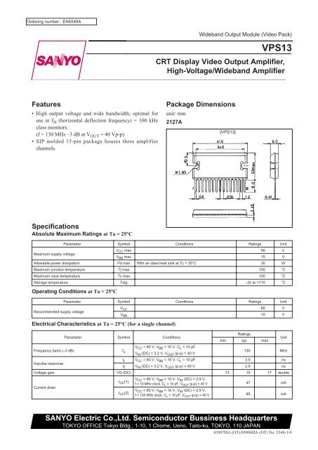
Ordering number : EN5548A<br />
<strong>Wideband</strong> <strong>Output</strong> Module (<strong>Video</strong> Pack)<br />
VPS13<br />
<strong>CRT</strong> <strong>Display</strong> <strong>Video</strong> <strong>Output</strong> <strong>Amplifier</strong>,<br />
<strong>High</strong>-<strong>Voltage</strong>/<strong>Wideband</strong> <strong>Amplifier</strong><br />
Features<br />
• <strong>High</strong> output voltage and wide bandwidth; optimal for<br />
use in f H (horizontal deflection frequency) = 100 kHz<br />
class monitors.<br />
(f = 130 MHz –3 dB at V OUT = 40 Vp-p)<br />
• SIP molded 15-pin package houses three amplifier<br />
channels.<br />
Package Dimensions<br />
unit: mm<br />
2127A<br />
[VPS13]<br />
Specifications<br />
Absolute Maximum Ratings at Ta = 25°C<br />
Parameter Symbol Conditions Ratings Unit<br />
V CC max 90 V<br />
Maximum supply voltage<br />
V BB max 15 V<br />
Allowable power dissipation Pd max With an ideal heat sink at Tc = 25°C 30 W<br />
Maximum junction temperature Tj max 150 °C<br />
Maximum case temperature Tc max 100 °C<br />
Storage temperature Tstg –20 to +110 °C<br />
Operating Conditions at Ta = 25°C<br />
Recommended supply voltage<br />
Parameter Symbol Conditions Ratings Unit<br />
Electrical Characteristics at Ta = 25°C (for a single channel)<br />
V CC 80 V<br />
V BB 10 V<br />
Parameter Symbol Conditions<br />
V CC = 80 V, V BB = 10 V, C L = 10 pF<br />
Frequency band (–3 dB) f c V IN (DC) = 3.2 V, V OUT (p-p) = 40 V<br />
Ratings<br />
min typ max<br />
Unit<br />
130 MHz<br />
t r V CC = 80 V, V BB = 10 V, C L = 10 pF 3.5 ns<br />
Impulse response<br />
t f V IN (DC) = 3.2 V, V OUT (p-p) = 40 V 2.9 ns<br />
<strong>Voltage</strong> gain VG (DC) 13 15 17 double<br />
Current drain<br />
I CC (1)<br />
I CC (2)<br />
V CC = 80 V, V BB = 10 V, V IN (DC) = 2.9 V,<br />
f = 10 MHz clock, C L = 10 pF, V OUT (p-p) = 40 V<br />
V CC = 80 V, V BB = 10 V, V IN (DC) = 2.9 V,<br />
f = 130 MHz clock, C L = 10 pF, V OUT (p-p) = 40 V<br />
47 mA<br />
85 mA<br />
SANYO Electric Co.,Ltd. Semiconductor Bussiness Headquarters<br />
TOKYO OFFICE Tokyo Bldg., 1-10, 1 Chome, Ueno, Taito-ku, TOKYO, 110 JAPAN<br />
83097HA (OT)/03096HA (OT) No. 5548-1/4
VPS13<br />
Internal Equivalent Circuit<br />
Test Circuit (for a single channel)<br />
No. 5548-2/4
VPS13<br />
Thermal Design<br />
Since the VPS13 includes three channels as shown in the circuit diagram on page 2, we first consider a single channel.<br />
The chip temperature of each transistor under actual operating conditions is determined using the following formula.<br />
Tj = (Tri) = θj-c (Tri) × Pc (Tri) + ∆Tc + Ta (°C) .......................(1)<br />
θj-c (Tri) : Thermal resistance of an individual transistor<br />
Pc(Tri) : Collector loss for an individual transistor<br />
∆Tc : Case temperature rise<br />
Ta : Ambient temperature<br />
The θj-c (Tri) for each chip is: θj-c (Tr1) = 35°C/W<br />
θj-c (Tr2) to (Tr4) = 30°C/W.......................................................(2)<br />
Although the loss for each transistor in a video pack varies with frequency and is not uniform, if we assume the<br />
maximum operating frequency, f = 130 MHz (clock), then the chip with the largest loss will be transistor 3 (Tr3) of the<br />
emitter-follower stage. From the Pd-f (clock) figure we see that loss will be 22% of the total loss for a single channel:<br />
Pc (emitter-follower stage) (f = 130 MHz) = Pd (1ch) (f = 130 MHz) × 0.22 [W] (3)<br />
Here, we must select a heat sink with a capacity θh such that the Tj of these transistors does not exceed 150°C. Equation<br />
(4) below gives the relationship between θh and ∆Tc.<br />
∆Tc = Pd (Total) × θh ..................................................................(4)<br />
The required θh is calculated using this equation and equation (1).<br />
No. 5548-3/4
VPS13<br />
VPS13 Thermal Design Example<br />
Conditions: Using an f H = 100 kHz class monitor, f V = 130 MHz (clock)<br />
V CC = 80 V, V BB = 10 V, V OUT = 40 Vp-p (C L = 10 pF)<br />
Here we consider the case where this class of monitor is operated up to Ta = 60°C at a maximum clock frequency of<br />
f = 130 MHz.<br />
As mentioned previously, the chip with the largest loss is transistor 3 (Tr3) of the emitter-follower stage. Determining<br />
that value gives:<br />
Pc (emitter-follower stage) = 6.8 × 0.22 ≈ 1.5 [W] .....................(5)<br />
Now, determine ∆Tj by substituting the value for θj-c in equation (5).<br />
∆Tj = 1.5 × 30 = 45 [°C]<br />
Here, ∆Tj < 50°C, and we need only consider cases where Tc < 100 °C. Therefore, we must design a θh for the heat sink<br />
such that the Tc < 100°C condition holds when three channels are operating at maximum levels, i.e., Pd(TOTAL) =<br />
Pd(one channel) × 3.<br />
∆Tc will be 100 – 60 = 40 °C, and therefore:<br />
θh = ∆Tc ÷ Pd (TOTAL) = 40 ÷ (6.8 × 3) = 2.0, i.e. θh = 2.0 °C/W<br />
In actual practice, the ambient temperature and operating conditions will allow a heat sink smaller than that indicated by<br />
this calculation to be used. Therefore, design optimization taking the actual conditions and the above data into account is<br />
also required.<br />
V CC (V) V BB (V) V OUT (V) V O (center)<br />
80 10 40 45<br />
■ No products described or contained herein are intended for use in surgical implants, life-support systems, aerospace<br />
equipment, nuclear power control systems, vehicles, disaster/crime-prevention equipment and the like, the failure of<br />
which may directly or indirectly cause injury, death or property loss.<br />
■ Anyone purchasing any products described or contained herein for an above-mentioned use shall:<br />
➀ Accept full responsibility and indemnify and defend SANYO ELECTRIC CO., LTD., its affiliates, subsidiaries and<br />
distributors and all their officers and employees, jointly and severally, against any and all claims and litigation and all<br />
damages, cost and expenses associated with such use:<br />
➁ Not impose any responsibility for any fault or negligence which may be cited in any such claim or litigation on<br />
SANYO ELECTRIC CO., LTD., its affiliates, subsidiaries and distributors or any of their officers and employees<br />
jointly or severally.<br />
■ Information (including circuit diagrams and circuit parameters) herein is for example only; it is not guaranteed for<br />
volume production. SANYO believes information herein is accurate and reliable, but no guarantees are made or implied<br />
regarding its use or any infringements of intellectual property rights or other rights of third parties.<br />
This catalog provides information as of August, 1997. Specifications and information herein are subject to<br />
change without notice.<br />
No. 5548-4/4