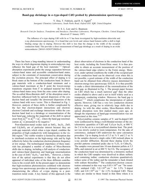
Band-gap shrinkage in n-type-doped CdO probed by photoemission ...
Band-gap shrinkage in n-type-doped CdO probed by photoemission ...
Band-gap shrinkage in n-type-doped CdO probed by photoemission ...
You also want an ePaper? Increase the reach of your titles
YUMPU automatically turns print PDFs into web optimized ePapers that Google loves.
RAPID COMMUNICATIONS<br />
PHYSICAL REVIEW B<br />
VOLUME 55, NUMBER 20<br />
15 MAY 1997-II<br />
<strong>Band</strong>-<strong>gap</strong> <strong>shr<strong>in</strong>kage</strong> <strong>in</strong> n-<strong>type</strong>-<strong>doped</strong> <strong>CdO</strong> <strong>probed</strong> <strong>by</strong> <strong>photoemission</strong> spectroscopy<br />
Y. Dou, T. Fishlock, and R. G. Egdell *<br />
Inorganic Chemistry Laboratory, South Parks Road, Oxford OX1 3QR, United K<strong>in</strong>gdom<br />
D. S. L. Law and G. Beamson<br />
Research Unit for Surfaces, Transforms and Interfaces, Daresbury Laboratory, Warr<strong>in</strong>gton, Cheshire, United K<strong>in</strong>gdom<br />
Received 27 January 1997<br />
The <strong>in</strong>fluence of n-<strong>type</strong> dop<strong>in</strong>g <strong>CdO</strong> with In or Y has been <strong>in</strong>vestigated <strong>by</strong> high-resolution ultraviolet and<br />
x-ray <strong>photoemission</strong> spectroscopy. It is found that core levels and valence band features suffer a shift to high<br />
b<strong>in</strong>d<strong>in</strong>g energy due to dop<strong>in</strong>g. However this shift is less than the change <strong>in</strong> the width of the occupied<br />
conduction band. This provides a direct measurement of band <strong>gap</strong> <strong>shr<strong>in</strong>kage</strong> as a result of dop<strong>in</strong>g <strong>in</strong> an oxide<br />
semiconductor. S0163-18299750820-4<br />
There has been a long-stand<strong>in</strong>g <strong>in</strong>terest <strong>in</strong> understand<strong>in</strong>g<br />
the ways <strong>in</strong> which degenerate dop<strong>in</strong>g <strong>in</strong> semiconductors may<br />
<strong>in</strong>fluence the band <strong>gap</strong> of the host materials. 1–3 Opticalabsorption<br />
experiments probe the energy separation between<br />
valence-band states and accessible conduction-band states,<br />
subject to the constra<strong>in</strong>t of momentum conservation dur<strong>in</strong>g<br />
the excitation process. The pr<strong>in</strong>cipal effect of dop<strong>in</strong>g is to<br />
block states at the bottom of the conduction band. In direct<strong>gap</strong><br />
materials with a conduction-band m<strong>in</strong>imum and a<br />
valence-band maximum at the po<strong>in</strong>t the lowest-energy<br />
transitions orig<strong>in</strong>ate from <strong>in</strong> un<strong>doped</strong> material but from<br />
valence-band states away from the zone center after dop<strong>in</strong>g.<br />
The so-called Moss-Burste<strong>in</strong> shift 1 of the absorption onset is<br />
therefore <strong>in</strong>fluenced both <strong>by</strong> upward dispersion of the conduction<br />
band and usually the downward dispersion of the<br />
valence band with wave vector. This is illustrated <strong>in</strong> Fig. 1.<br />
However, analysis of these shifts is further complicated <strong>by</strong><br />
the fact that electron-dopant <strong>in</strong>teractions and electronelectron<br />
Coulomb and exchange <strong>in</strong>teractions with<strong>in</strong> the conduction<br />
band lead to a <strong>shr<strong>in</strong>kage</strong> or renormalization of the<br />
host band <strong>gap</strong>, reduc<strong>in</strong>g the magnitude of the shift <strong>in</strong> optical<br />
onset from BM g to BM g N g , where the band <strong>gap</strong> renormalization<br />
N g is presumed to be negative. 3<br />
Post-transition-metal oxides such as SnO 2 ,In 2 O 3 , ZnO,<br />
and Cd 2 SnO 4 are of particular <strong>in</strong>terest because they are<br />
wide-<strong>gap</strong> materials which when n-<strong>type</strong> <strong>doped</strong>, comb<strong>in</strong>e the<br />
properties of high conductivity with transparency <strong>in</strong> the visible<br />
region. 4 The visible w<strong>in</strong>dow is limited <strong>by</strong> absorption due<br />
to <strong>in</strong>terband excitation on the high-energy side and <strong>by</strong> high<br />
reflectivity below the conduction electron plasmon frequency<br />
at low energy. The technological importance of these materials<br />
has prompted a number of studies of Moss-Burste<strong>in</strong><br />
shifts due to dop<strong>in</strong>g, <strong>in</strong>clud<strong>in</strong>g a full analysis of conductionand<br />
valence-band dispersion and band-<strong>gap</strong> renormalization<br />
<strong>in</strong> the case of ZnO, 5 In 2 O 3 , 6 and SnO 2 . 7 However, a limitation<br />
of the optical experiments is that they do not allow<br />
appraisal of <strong>in</strong>dividual roles of the three different contributions<br />
to the overall shift. In the present paper we demonstrate<br />
that high-resolution <strong>photoemission</strong> comb<strong>in</strong>ed with electronenergy-loss<br />
spectroscopy provides an alternative approach to<br />
characteriz<strong>in</strong>g the effects of n-<strong>type</strong> dop<strong>in</strong>g <strong>in</strong> a posttransition<br />
metal oxide. A key feature of this approach is the<br />
direct observation of electrons <strong>in</strong> the conduction band of the<br />
host oxide, <strong>in</strong>clud<strong>in</strong>g the Fermi-Dirac onset. It is thus possible<br />
to obta<strong>in</strong> an accurate measurement of the position of<br />
the valence-band edge relative to the Fermi energy. Moreover,<br />
under optimal conditions the width of the occupied part<br />
of the conduction band can be observed: even when this is<br />
not possible, a good estimate of the width of the conduction<br />
band can be obta<strong>in</strong>ed from effective masses determ<strong>in</strong>ed <strong>by</strong><br />
electron-energy-loss spectroscopy EELS. It is thus possible<br />
to make a direct determ<strong>in</strong>ation of the renormalization of the<br />
band <strong>gap</strong>, as illustrated <strong>in</strong> Fig. 1. The present paper focuses<br />
on <strong>CdO</strong> which has a much narrower <strong>gap</strong> 8 than the other<br />
oxides alluded to above and is not <strong>in</strong> itself widely used as a<br />
transparent, conduct<strong>in</strong>g w<strong>in</strong>dow. Moreover, the band <strong>gap</strong> is<br />
<strong>in</strong>direct, 9–11 which complicates the <strong>in</strong>terpretation of optical<br />
spectra. However, <strong>CdO</strong> has a very low conduction electron<br />
effective mass, giv<strong>in</strong>g rise to relatively large shifts due to<br />
dop<strong>in</strong>g. As with the other oxides, Moss-Burste<strong>in</strong> shifts <strong>in</strong><br />
optical absorption were first studied many years ago, although<br />
the importance of band-<strong>gap</strong> renormalization was not<br />
appreciated at this time. 12,13<br />
Polycrystall<strong>in</strong>e ceramic samples of Y- and In-<strong>doped</strong> <strong>CdO</strong><br />
were synthesized <strong>by</strong> fir<strong>in</strong>g a well-blended mixture of the stoichiometric<br />
quantities of <strong>CdO</strong> and Y 2 O 3 or In 2 O 3 at 880 °C<br />
for2d<strong>in</strong>theair<strong>in</strong>arecrystallized alum<strong>in</strong>a boat. The product<br />
was slowly cooled to room temperature. For the sake of<br />
consistency, un<strong>doped</strong> <strong>CdO</strong> underwent the same calc<strong>in</strong>ation<br />
procedure. Up to dop<strong>in</strong>g levels of 3.5 at. % Y and 2.3 at. %<br />
In the samples showed a s<strong>in</strong>gle cubic <strong>CdO</strong> rocksalt phase <strong>in</strong><br />
x-ray powder diffraction. Beyond these dop<strong>in</strong>g levels the<br />
powder patterns conta<strong>in</strong>ed peaks due to Y 2 O 3 or CdIn 2 O 4 .<br />
The samples were pressed <strong>in</strong>to 10 mm diameter pellets at 5.5<br />
MPa, and s<strong>in</strong>tered <strong>in</strong> air at 880 °C for 8 h. The occupancy of<br />
the conduction band was determ<strong>in</strong>ed <strong>by</strong> a titrimetric method<br />
<strong>in</strong> which the <strong>CdO</strong> samples were dissolved <strong>in</strong> dilute sulfuric<br />
acid conta<strong>in</strong><strong>in</strong>g iod<strong>in</strong>e: conduction electrons quantitatively<br />
reduce some of the iod<strong>in</strong>e and the rema<strong>in</strong>der is back titrated<br />
with sodium thiosulfate. 14 The conduction-electron concentration<br />
estimated <strong>in</strong> this way was 0.8510 20 cm 3 for nom<strong>in</strong>ally<br />
un<strong>doped</strong> <strong>CdO</strong>, 3.810 20 cm 3 for 3.5% Y-<strong>doped</strong><br />
<strong>CdO</strong>, and 4.810 20 cm 3 for 2.3% In-<strong>doped</strong> <strong>CdO</strong>. These<br />
values are similar to those found <strong>in</strong> th<strong>in</strong> films where it is<br />
0163-1829/97/5520/133814/$10.00 55 R13 381 © 1997 The American Physical Society
RAPID COMMUNICATIONS<br />
R13 382 DOU, FISHLOCK, EGDELL, LAW, AND BEAMSON<br />
55<br />
FIG. 1. Schematic energy-level diagrams show<strong>in</strong>g effects of degenerate n-<strong>type</strong> dop<strong>in</strong>g <strong>in</strong> an oxide semiconductor. a Nom<strong>in</strong>ally un<strong>doped</strong><br />
oxide with a direct optical band <strong>gap</strong> g0 .b Doped oxide <strong>in</strong> which the optical <strong>gap</strong> has <strong>in</strong>creased <strong>by</strong> g BM due to block<strong>in</strong>g of states at the<br />
bottom of the conduction band. The shift depends on both conduction and valence-band dispersion. c Optical <strong>gap</strong> after band <strong>gap</strong> <strong>shr<strong>in</strong>kage</strong>.<br />
The new <strong>gap</strong> is seen to depend on both g BM and g N and the <strong>in</strong>dividual contributions to the new <strong>gap</strong> cannot be determ<strong>in</strong>ed <strong>by</strong> optical<br />
absorption. d An illustration of the quantities which can be measured <strong>in</strong> the present experiment. These <strong>in</strong>clude the position of the<br />
valence-band-edge relative to the Fermi level E VB and the width of the occupied conduction-band E f . The renormalized band <strong>gap</strong> E g0<br />
g N can also be determ<strong>in</strong>ed.<br />
presumed that <strong>in</strong> the nom<strong>in</strong>ally un<strong>doped</strong> material the conduction<br />
electrons are associated with <strong>in</strong>terstitial Cd donors.<br />
Electron spectra were measured <strong>in</strong> two <strong>in</strong>struments. The<br />
first is an ESCALAB with facilities for excitation of <strong>photoemission</strong><br />
spectra us<strong>in</strong>g unmonochromated AlK or MgK x-<br />
rays or UV radiation from a noble-gas discharge lamp.<br />
Sample clean<strong>in</strong>g was achieved <strong>by</strong> anneal<strong>in</strong>g pellets for 2hat<br />
around 400 °C stub temperature <strong>in</strong> the spectrometer preparation<br />
chamber base pressure 10 9 mbar. X-ray <strong>photoemission</strong><br />
spectra XPS were found to be completely free of<br />
signals due to carbon or other contam<strong>in</strong>ation. The nom<strong>in</strong>al<br />
analyzer resolution was set at 100 meV for HeI <strong>photoemission</strong><br />
measurements. Procedures for stripp<strong>in</strong>g spectra of structure<br />
due to satellite radiation and for spectral calibration <strong>in</strong><br />
this measurement have been described <strong>in</strong> detail elsewhere. 15<br />
Energy-loss spectra were measured <strong>in</strong> the same spectrometer<br />
us<strong>in</strong>g an <strong>in</strong>cident electron beam derived from an electron gun<br />
usually used for low-energy electron diffraction LEED<br />
studies, aga<strong>in</strong> as described elsewhere. 15 The second <strong>in</strong>strument<br />
is a Scienta ESCA 300 XPS spectrometer <strong>in</strong>corporat<strong>in</strong>g<br />
a rotat<strong>in</strong>g anode x-ray source with seven-crystal x-ray monochromator,<br />
300 mm mean radius electron-energy analyzer,<br />
and parallel electron-detection system. The overall effective<br />
resolution <strong>in</strong> this <strong>in</strong>strument was 350 meV. The <strong>in</strong>strument is<br />
regularly calibrated us<strong>in</strong>g the Fermi level and core levels<br />
from an ion-bombarded silver foil. The clean<strong>in</strong>g procedures<br />
<strong>in</strong> the Scienta spectrometer were similar to those <strong>in</strong> the ES-<br />
CALAB, except that heat<strong>in</strong>g was via a resistive P8 probe<br />
heater.<br />
Figure 2 shows UV <strong>photoemission</strong> spectra of nom<strong>in</strong>ally<br />
un<strong>doped</strong> <strong>CdO</strong> and of maximally Y- and In-<strong>doped</strong> <strong>CdO</strong> <strong>in</strong> the<br />
b<strong>in</strong>d<strong>in</strong>g energy range up to 4 eV. This region encompasses<br />
the conduction-band, bulk band <strong>gap</strong>, and valence-band edge.<br />
Straddl<strong>in</strong>g zero-b<strong>in</strong>d<strong>in</strong>g-energy is a Fermi-Dirac-like cutoff<br />
associated with electrons <strong>in</strong> the Cd 5s conduction band. The<br />
FIG. 2. HeI <strong>photoemission</strong> spectra of a nom<strong>in</strong>ally-un<strong>doped</strong><br />
<strong>CdO</strong>, b 3.5% Y-<strong>doped</strong> <strong>CdO</strong>, and c 2.3% In-<strong>doped</strong> <strong>CdO</strong>. Structure<br />
due to satellite radiation has been stripped from the spectra.<br />
B<strong>in</strong>d<strong>in</strong>g energies are relative to the Fermi energy, which is <strong>in</strong>dicated<br />
<strong>by</strong> bold vertical l<strong>in</strong>es. The positions of the O 2p valence-band<br />
edges determ<strong>in</strong>ed <strong>by</strong> a l<strong>in</strong>ear extrapolation procedure are <strong>in</strong>dicated<br />
with bold dashed l<strong>in</strong>es. The positions of the bottoms of the conduction<br />
bands estimated from measured surface-plasma energies<br />
through application of Eq. 5 are <strong>in</strong>dicated <strong>by</strong> light dashed l<strong>in</strong>es.
RAPID COMMUNICATIONS<br />
55 BAND-GAP SHRINKAGE IN n-TYPE-DOPED <strong>CdO</strong> ...<br />
R13 383<br />
conduction-band feature is much weaker and narrower <strong>in</strong> the<br />
nom<strong>in</strong>ally un<strong>doped</strong> <strong>CdO</strong> than for the Y- or In-<strong>doped</strong><br />
samples, <strong>in</strong> accordance with the lower-carrier concentration.<br />
Moreover when b<strong>in</strong>d<strong>in</strong>g energies are referred to the Fermi<br />
level it is clear that the valence-band edge shows the expected<br />
shift to high-b<strong>in</strong>d<strong>in</strong>g energy due to the fill<strong>in</strong>g of the<br />
conduction band <strong>in</strong> the <strong>doped</strong> samples. This conclusion is<br />
confirmed <strong>by</strong> high-resolution XPS. Here it is found that both<br />
the valence-band edge and peaks <strong>in</strong> the valence band show<br />
shifts to high b<strong>in</strong>d<strong>in</strong>g energy with dop<strong>in</strong>g, as illustrated <strong>in</strong><br />
Fig. 3, where the shift of a sharp valence-band peak at about<br />
6 eV b<strong>in</strong>d<strong>in</strong>g energy is highlighted. Moreover the 4d corelevel<br />
peaks also show pronounced shifts. A complete set of<br />
b<strong>in</strong>d<strong>in</strong>g energies is given <strong>in</strong> Table I, where it is seen that<br />
with<strong>in</strong> the experimental uncerta<strong>in</strong>ty of about 0.05 eV all<br />
three features alluded to above show the same shift.<br />
In order to understand the magnitude of the shifts, it is<br />
necessary to consider the widths of the occupied part of the<br />
conduction band. In a simple free-electron model the occupied<br />
bandwidth is given <strong>by</strong> E f where,<br />
E f 2<br />
h 2 3 2 N 2/3<br />
. 1<br />
2m*<br />
Here m* is the electron effective mass and N is the carrier<br />
concentration.<br />
However, it is well known for narrow-<strong>gap</strong> oxides such as<br />
<strong>CdO</strong> that the effective mass varies strongly as a function of<br />
carrier concentration. We have, therefore, used EELS to<br />
probe effective-mass variations. Typical energy-loss spectra<br />
excited at 200 eV beam energy are shown <strong>in</strong> Fig. 4. At low<br />
energy, a well-def<strong>in</strong>ed peak is observed with the <strong>in</strong>tensity of<br />
the order expected 16 for pure surface loss as opposed to bulk<br />
loss. The surface-loss frequency is given <strong>by</strong><br />
2 sp <br />
Ne 2<br />
0 1 ,<br />
where e is the electronic charge, 0 is the permittivity of free<br />
space, and is the high-frequency dielectric constant<br />
which is known to be 5.0. The plasmon is built up from<br />
electron-hole excitations centered around the Fermi energy 17<br />
and the effective mass relevant to EELS therefore depends<br />
on the dispersion of energy with wave vector at E f ,<br />
2<br />
FIG. 3. High-resolution valence-band XPS excited with monochromatized<br />
Al K x-rays for a nom<strong>in</strong>ally-un<strong>doped</strong> <strong>CdO</strong>, b<br />
3.5% Y-<strong>doped</strong> <strong>CdO</strong>, and c 2.3% In-<strong>doped</strong> <strong>CdO</strong>. B<strong>in</strong>d<strong>in</strong>g energies<br />
are given relative to the Fermi energy which is <strong>in</strong>dicated <strong>by</strong> a solid<br />
l<strong>in</strong>e. Note the shift <strong>in</strong> the sharp valence-band peak at about 6 eV<br />
b<strong>in</strong>d<strong>in</strong>g energy.<br />
dE<br />
dkEE f<br />
2<br />
h 2 k f<br />
m* . 3<br />
We have found from an extensive series of measurements <strong>in</strong><br />
EELS of surface-plasmon energies at different dop<strong>in</strong>g levels<br />
that the effective mass shows an essentially l<strong>in</strong>ear variation<br />
with carrier concentration N,<br />
m*m 0<br />
*cN,<br />
4<br />
TABLE I. B<strong>in</strong>d<strong>in</strong>g energies and bandwidths <strong>in</strong> n-<strong>type</strong>-<strong>doped</strong> <strong>CdO</strong>. a,b<br />
<strong>CdO</strong> 3.5% Y-<strong>doped</strong> <strong>CdO</strong> 2.3% In-<strong>doped</strong> <strong>CdO</strong><br />
Valence-band onset 1.530.05 1.960.05 0.43 2.170.05 0.64<br />
Valence-band peak<br />
5.400.05 5.900.05 0.50 6.000.05 0.60<br />
BE c<br />
Cd 4d core-level BE 10.600.05 11.050.05 0.45 11.250.05 0.65<br />
Conduction-band<br />
width estimated from<br />
EELS data d 0.54 1.19 0.65 1.32 0.78<br />
a All values are <strong>in</strong> eV.<br />
b Figure <strong>in</strong> parentheses give shifts relative to <strong>CdO</strong>.<br />
c Valence-band peak highlighted <strong>in</strong> Fig. 2.<br />
d The effective mass is assumed to vary with<strong>in</strong> the conduction band <strong>in</strong> accordance with Eq. 4.
RAPID COMMUNICATIONS<br />
R13 384 DOU, FISHLOCK, EGDELL, LAW, AND BEAMSON<br />
55<br />
FIG. 4. Energy-loss spectra of a nom<strong>in</strong>ally-un<strong>doped</strong> <strong>CdO</strong>, b<br />
3.5% Y-<strong>doped</strong> <strong>CdO</strong>, and c 2.3% In-<strong>doped</strong> <strong>CdO</strong> excited with 200<br />
eV electron beam show<strong>in</strong>g loss peaks due to excitation of<br />
conduction-electron surface plasmons.<br />
where c is a constant. Experimentally we f<strong>in</strong>d m 0<br />
*/m 0<br />
0.121 and c/m 0 0.031510 20 cm 3 , where m 0 is the<br />
electron rest mass. This l<strong>in</strong>ear variation is <strong>in</strong> agreement with<br />
previous work. 13 The Fermi energy now depends on the <strong>in</strong>tegral<br />
N h<br />
E f 2<br />
0 43 2 n 1/3 m 0<br />
*cn dn. 5<br />
The calculated conduction-band widths obta<strong>in</strong>ed <strong>in</strong> this way<br />
are given <strong>in</strong> Table I. The variation of m* with<strong>in</strong> the band<br />
gives rise to much broader conduction bands than would be<br />
expected if the mass at the Fermi level applied throughout<br />
the band. The calculated bandwidths are also <strong>in</strong>dicated on<br />
Fig. 2. The agreement with experiment is satisfactory, subject<br />
to the reservation that it is difficult to def<strong>in</strong>e the position<br />
of the bottom of the conduction band <strong>in</strong> nom<strong>in</strong>ally un<strong>doped</strong><br />
<strong>CdO</strong> due to its very weak <strong>in</strong>tensity and the occurrence of<br />
states <strong>in</strong> the bulk band <strong>gap</strong> just above the valence-band edge.<br />
These probably arise from Cd atoms <strong>in</strong> surface sites where<br />
5s-5p mix<strong>in</strong>g <strong>in</strong>duced <strong>by</strong> the electric-field gradient at the<br />
surface pushes Cd 5s states down <strong>in</strong>to the band <strong>gap</strong> to give a<br />
doubly occupied sp hybrid state: similar states exist on<br />
SnO 2 surfaces. 18 Despite this difficulty, it is clear that the<br />
b<strong>in</strong>d<strong>in</strong>g-energy shifts of the valence-band edges <strong>in</strong> In- and<br />
Y-<strong>doped</strong> <strong>CdO</strong> are significantly less than expected from the<br />
<strong>in</strong>creased width of the conduction band. The discrepancies<br />
correspond to the <strong>shr<strong>in</strong>kage</strong> of the band <strong>gap</strong>, which is thus<br />
estimated to be 0.220.05 eV for 3.5% Y-<strong>doped</strong> <strong>CdO</strong> and<br />
0.140.15 eV for 2.3% In-<strong>doped</strong> <strong>CdO</strong>. These estimates are<br />
of the order of magnitude expected from calculations 6 on<br />
Sn-<strong>doped</strong> In 2 O 3 us<strong>in</strong>g He<strong>in</strong>e-Abarenkov pseudopotentials to<br />
deal with the electron impurity <strong>in</strong>teraction and the randomphase<br />
approximation to account for electron-electron <strong>in</strong>teractions.<br />
In this work it was found that at a carrier concentration<br />
of 410 20 cm 3 the contributions to the band <strong>gap</strong> narrow<strong>in</strong>g<br />
from electron-impurity and electron-electron <strong>in</strong>teractions<br />
were about 0.05 and 0.2 eV, respectively.<br />
In summary, we have developed a method for measur<strong>in</strong>g<br />
the band <strong>gap</strong> <strong>shr<strong>in</strong>kage</strong> <strong>in</strong> degenerately <strong>doped</strong> oxide semiconductors<br />
and have applied this technique to <strong>CdO</strong>. It should<br />
be straightforward to extend this approach to other oxides<br />
such as SnO 2 and In 2 O 3 .<br />
* Author to whom correspondence should be sent. Electronic address:<br />
Egdell@erm<strong>in</strong>e.ox.ac.uk<br />
1 E. Burste<strong>in</strong>, Phys. Rev. 93, 632 1954.<br />
2 R. A. Abram, G. J. Ress, and B. L. H. Wilson, Adv. Phys. 27, 799<br />
1978.<br />
3 K. F. Berggren and B. E. Sernelius, Phys. Rev. B 24, 1971<br />
1981.<br />
4 H. Köstl<strong>in</strong>, Festkoerperprobleme 22, 229 1982.<br />
5 Z. C. J<strong>in</strong>, I. Hamberg, C. G. Granquist, B. E. Sernelius, and K. F.<br />
Berggren, Th<strong>in</strong> Solid Films 164, 381 1988.<br />
6 I. Hamberg, K. F. Berggren, L. Engstrom, C. G. Granquist, and B.<br />
E. Sernelius, Phys. Rev. B 30, 3240 1984.<br />
7 G. Sanon, R. Rup, and A. Mans<strong>in</strong>gh, Phys. Rev. B 44, 5672<br />
1991.<br />
8 H. F<strong>in</strong>kenrath, <strong>in</strong> Physics of II-VI and I-VII Compounds, Semimagnetic,<br />
Semiconductors, edited <strong>by</strong> O. Madelung, M. Schulz,<br />
and H. Weiss, Landolt-Börnste<strong>in</strong>, New Series, Group III, Vol.<br />
17 Spr<strong>in</strong>ger-Verlag, Berl<strong>in</strong>, 1982, p. 162 and references<br />
there<strong>in</strong>.<br />
9 H. Köhler, Solid State Commun. 11, 1687 1972.<br />
10 J. C. Boettger and A. B. Kunz, Phys. Rev. B 27, 1359 1982.<br />
11 J. E. Jaffe, R. Pandey, and A. B. Kunz, Phys. Rev. B 43, 14 030<br />
1991.<br />
12 H. F<strong>in</strong>kenrath, Z. Phys. 159, 112 1960.<br />
13 H. F<strong>in</strong>kenrath and M. von Ortenberg, Z. Angew. Phys. 23, 323<br />
1967.<br />
14 M. P. Shatlock and G. E. Machiel, J. Chem. Phys. 81, 859 1984.<br />
15 Y. Dou and R. G. Egdell, Phys. Rev. B 53, 15 405 1996.<br />
16 H. Ibach and D. L. Mills, Electron Energy Loss Spectroscopy and<br />
Surface Vibrations Academic, New York, 1982.<br />
17 T. Inaoka, D. M. Newns, and R. G. Egdell, Surf. Sci. 186, 290<br />
1987.<br />
18 I. Manassidis, J. Goniakowski, L. N. Kantorovitch, and M. J.<br />
Gillan, Surf. Sci. 339, 258 1995.


