Datasheet Download
Datasheet Download
Datasheet Download

You also want an ePaper? Increase the reach of your titles
YUMPU automatically turns print PDFs into web optimized ePapers that Google loves.
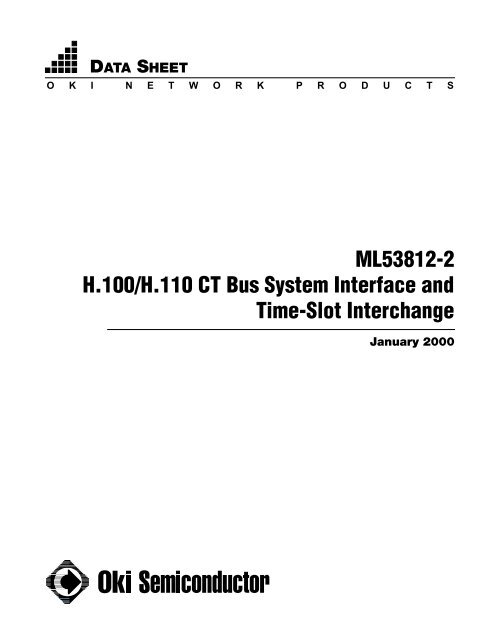
DATA SHEET<br />
O K I N E T W O R K P R O D U C T S<br />
ML53812-2<br />
H.100/H.110 CT Bus System Interface and<br />
Time-Slot Interchange<br />
January 2000
Revision History<br />
September 1999 320101-005 Previous Release<br />
January 2000 320101-006 Timing tables altered on page 50:<br />
“Local Clock and Frame Synchronization Timing”,<br />
“Local Clock to CT Bus Clock Skew”, and<br />
“Local Serial Stream Timing”<br />
Timing diagram (Figure 11) atered on page 51:<br />
“Local Clock and Frame Synchronization Timing”<br />
Oki Semiconductor
Contents<br />
Description . . . . . . . . . . . . . . . . . . . . . . . . . . . . . . . . . . . . . . . . . . . . . . . . . . . . . . . . . . . . . . . . . . . . . . . . . . . . . . . . 1<br />
Features . . . . . . . . . . . . . . . . . . . . . . . . . . . . . . . . . . . . . . . . . . . . . . . . . . . . . . . . . . . . . . . . . . . . . . . . . . . . . . . . . . 2<br />
Applications . . . . . . . . . . . . . . . . . . . . . . . . . . . . . . . . . . . . . . . . . . . . . . . . . . . . . . . . . . . . . . . . . . . . . . . . . . . 2<br />
Pin Configuration . . . . . . . . . . . . . . . . . . . . . . . . . . . . . . . . . . . . . . . . . . . . . . . . . . . . . . . . . . . . . . . . . . . . . . . . . . . 3<br />
ML53812-2 176-Pin LQFP Pin Assignment . . . . . . . . . . . . . . . . . . . . . . . . . . . . . . . . . . . . . . . . . . . . . . . . . . . 4<br />
Signal descriptions . . . . . . . . . . . . . . . . . . . . . . . . . . . . . . . . . . . . . . . . . . . . . . . . . . . . . . . . . . . . . . . . . . . . . . . . . . 5<br />
Functional Description . . . . . . . . . . . . . . . . . . . . . . . . . . . . . . . . . . . . . . . . . . . . . . . . . . . . . . . . . . . . . . . . . . . . . . . 7<br />
Local Bus . . . . . . . . . . . . . . . . . . . . . . . . . . . . . . . . . . . . . . . . . . . . . . . . . . . . . . . . . . . . . . . . . . . . . . . . . . . . . 7<br />
CT Bus . . . . . . . . . . . . . . . . . . . . . . . . . . . . . . . . . . . . . . . . . . . . . . . . . . . . . . . . . . . . . . . . . . . . . . . . . . . . . . . 8<br />
Test Access Port . . . . . . . . . . . . . . . . . . . . . . . . . . . . . . . . . . . . . . . . . . . . . . . . . . . . . . . . . . . . . . . . . . . . . . . 8<br />
Pin Continuity Test . . . . . . . . . . . . . . . . . . . . . . . . . . . . . . . . . . . . . . . . . . . . . . . . . . . . . . . . . . . . . . . . . . . . . . 8<br />
Analog PLL Test . . . . . . . . . . . . . . . . . . . . . . . . . . . . . . . . . . . . . . . . . . . . . . . . . . . . . . . . . . . . . . . . . . . . . . . . 8<br />
Microprocessor Interface . . . . . . . . . . . . . . . . . . . . . . . . . . . . . . . . . . . . . . . . . . . . . . . . . . . . . . . . . . . . . . . . . 8<br />
Analog PLL . . . . . . . . . . . . . . . . . . . . . . . . . . . . . . . . . . . . . . . . . . . . . . . . . . . . . . . . . . . . . . . . . . . . . . . . . . . . 9<br />
Slave PLL . . . . . . . . . . . . . . . . . . . . . . . . . . . . . . . . . . . . . . . . . . . . . . . . . . . . . . . . . . . . . . . . . . . . . . . . . . . . . 9<br />
Master PLL . . . . . . . . . . . . . . . . . . . . . . . . . . . . . . . . . . . . . . . . . . . . . . . . . . . . . . . . . . . . . . . . . . . . . . . . . . . . 9<br />
Reference Master . . . . . . . . . . . . . . . . . . . . . . . . . . . . . . . . . . . . . . . . . . . . . . . . . . . . . . . . . . . . . . . . . . . . . . 10<br />
Local Clock and Frame Sync . . . . . . . . . . . . . . . . . . . . . . . . . . . . . . . . . . . . . . . . . . . . . . . . . . . . . . . . . . . . . 10<br />
Local Streams . . . . . . . . . . . . . . . . . . . . . . . . . . . . . . . . . . . . . . . . . . . . . . . . . . . . . . . . . . . . . . . . . . . . . . . . 10<br />
CT Bus Streams . . . . . . . . . . . . . . . . . . . . . . . . . . . . . . . . . . . . . . . . . . . . . . . . . . . . . . . . . . . . . . . . . . . . . . . 11<br />
CT_D disable . . . . . . . . . . . . . . . . . . . . . . . . . . . . . . . . . . . . . . . . . . . . . . . . . . . . . . . . . . . . . . . . . . . . . . . . . 11<br />
Diagnostic Mode . . . . . . . . . . . . . . . . . . . . . . . . . . . . . . . . . . . . . . . . . . . . . . . . . . . . . . . . . . . . . . . . . . . . . . 11<br />
Interrupts . . . . . . . . . . . . . . . . . . . . . . . . . . . . . . . . . . . . . . . . . . . . . . . . . . . . . . . . . . . . . . . . . . . . . . . . . . . . 11<br />
GPIO Ports . . . . . . . . . . . . . . . . . . . . . . . . . . . . . . . . . . . . . . . . . . . . . . . . . . . . . . . . . . . . . . . . . . . . . . . . . . . 12<br />
Message Channel . . . . . . . . . . . . . . . . . . . . . . . . . . . . . . . . . . . . . . . . . . . . . . . . . . . . . . . . . . . . . . . . . . . . . 12<br />
Registers . . . . . . . . . . . . . . . . . . . . . . . . . . . . . . . . . . . . . . . . . . . . . . . . . . . . . . . . . . . . . . . . . . . . . . . . . . . . . . . . 13<br />
Microprocessor Address Map . . . . . . . . . . . . . . . . . . . . . . . . . . . . . . . . . . . . . . . . . . . . . . . . . . . . . . . . . . . . 13<br />
Command/Status Register . . . . . . . . . . . . . . . . . . . . . . . . . . . . . . . . . . . . . . . . . . . . . . . . . . . . . . . . . . . . . . . 14<br />
Internal Address Map . . . . . . . . . . . . . . . . . . . . . . . . . . . . . . . . . . . . . . . . . . . . . . . . . . . . . . . . . . . . . . . . . . 15<br />
Configuration Registers . . . . . . . . . . . . . . . . . . . . . . . . . . . . . . . . . . . . . . . . . . . . . . . . . . . . . . . . . . . . . . . . . 16<br />
Device ID Registers (Read Only) . . . . . . . . . . . . . . . . . . . . . . . . . . . . . . . . . . . . . . . . . . . . . . . . . . . . . . . . . . 37<br />
Stream Switch Routing Registers, AR = 1007h:1000h (Ch. 7:0) . . . . . . . . . . . . . . . . . . . . . . . . . . . . . . . . . . 38<br />
Stream Switch Connection Mapping . . . . . . . . . . . . . . . . . . . . . . . . . . . . . . . . . . . . . . . . . . . . . . . . . . . . . . . 39<br />
Transmit Switch Routing Registers, AR = 20ffh:2000h (Ch. 255:0) . . . . . . . . . . . . . . . . . . . . . . . . . . . . . . . . 41<br />
Receive Switch Routing Registers, AR = 30ffh:3000h (Ch. 255:0) . . . . . . . . . . . . . . . . . . . . . . . . . . . . . . . . 43<br />
Indirect Transmit Switch Parallel Access Registers, AR = 40ffh:4000h (Ch. 255:0) . . . . . . . . . . . . . . . . . . . 45<br />
Indirect Receive Switch Parallel Access Registers, AR = 50ffh:5000h (Ch. 255:0) . . . . . . . . . . . . . . . . . . . . 45<br />
Electrical Specifications . . . . . . . . . . . . . . . . . . . . . . . . . . . . . . . . . . . . . . . . . . . . . . . . . . . . . . . . . . . . . . . . . . . . . 46<br />
Absolute Maximum Ratings . . . . . . . . . . . . . . . . . . . . . . . . . . . . . . . . . . . . . . . . . . . . . . . . . . . . . . . . . . . . . . 46<br />
Recommended Operating Conditions . . . . . . . . . . . . . . . . . . . . . . . . . . . . . . . . . . . . . . . . . . . . . . . . . . . . . . 46<br />
DC Electrical Characteristics . . . . . . . . . . . . . . . . . . . . . . . . . . . . . . . . . . . . . . . . . . . . . . . . . . . . . . . . . . . . . 46<br />
AC Electrical Characteristics . . . . . . . . . . . . . . . . . . . . . . . . . . . . . . . . . . . . . . . . . . . . . . . . . . . . . . . . . . . . . 47<br />
H.100/H.110 Bus Timing Specification . . . . . . . . . . . . . . . . . . . . . . . . . . . . . . . . . . . . . . . . . . . . . . . . . . . . . . 54<br />
Clock Skew Requirements . . . . . . . . . . . . . . . . . . . . . . . . . . . . . . . . . . . . . . . . . . . . . . . . . . . . . . . . . . . . . . . 56<br />
ML53812-2 Package specifications . . . . . . . . . . . . . . . . . . . . . . . . . . . . . . . . . . . . . . . . . . . . . . . . . . . . . . . . . . . . 57<br />
LQFP176 Package Outlines and Dimensions . . . . . . . . . . . . . . . . . . . . . . . . . . . . . . . . . . . . . . . . . . . . . . . . 57<br />
LQFP176 Mounting Pad Reference Measurements . . . . . . . . . . . . . . . . . . . . . . . . . . . . . . . . . . . . . . . . . . . 58<br />
Oki Semiconductor
■ ■ –––––––––––––––––––––––––––––––––––––––––––––––––––––––––––––––––––––––––––––––––––––––––––<br />
Oki Semiconductor
ML53812-2<br />
H.100/H.110CT Bus System Interface and Time Slot Interchange<br />
1.0 DESCRIPTION<br />
The ML53812-2 is a complete CT Bus system interface and time slot interchange device that provides a<br />
cost-effective connection between a computer board’s telephony interfaces or signal processing resources<br />
and the CT Bus. The ML53812-2 is an evolution of existing time-slot interchange ICs which offers seamless<br />
interoperability with SCbus devices.<br />
A key element in computer telephony (CT) equipment is the auxiliary telecom bus. Most manufacturers<br />
of high-capacity CT equipment have used one or more types of telecom buses to transport and switch<br />
low-latency communications traffic between boards within the computer, bypassing the computer’s<br />
main I/O and memory buses. To simplify the integration of devices that incorporate a telecom bus, the<br />
Enterprise Computer Telephony Forum (ECTF) developed a standard bus (H.100/H.110 CT Bus) that<br />
provides compatibility modes with the most prevalent telecom buses today (SCbus and MVIP-90),<br />
as well as the capacity and feature set needed to support the next generation of high capacity CT servers.<br />
The new CT Bus is embraced by Dialogic under the Signal Computing System Architecture (SCSA)<br />
umbrella of open standards for building interoperable CT systems.<br />
The ML53812-2 runs in both 4 MHz and 8 MHz SCbus modes and supports the switching features<br />
needed to integrate CT Bus devices with 4 MHz SCbus, 8 MHz SCbus, and 2 MHz MVIP-90 devices.<br />
Because the H.100/H.110 CT Bus uses an identical switching model and clock speeds to that used for the<br />
SCbus, developers have unparalleled flexibility in integrating these two types of devices, or in transitioning<br />
from one type to the other.<br />
The ML53812-2 takes full advantage of the mandatory and optional features defined in the ECTF H.100<br />
and H.110 interoperability specifications. It is a non-blocking 512 x 4096 time slot switch, interfacing up<br />
to 512 ports on its parent device to any of the 4096 time slots on the new CT Bus. The high number of local<br />
time slots available makes it easier to design high-density CT hardware, supporting as many as eight network<br />
interfaces or 256 voice processing ports per chip.<br />
This powerful chip is offered in an ultra slim profile (176-pin LQFP package, with a 24 mm x 24 mm x 1.4<br />
mm body size) that makes it possible to mount the chip on either side of the board. The chip is fully software<br />
programmable, and can be controlled by a variety of microprocessors, including Intel and Motorola<br />
in both multiplexed and nonmultiplexed modes.<br />
Oki Semiconductor<br />
1
■ ML53812-2 ■ ––––––––––––––––––––––––––––––––––––––––––––––––––––––––––––––––––––––––––––––––––<br />
2.0 FEATURES<br />
• High functionality, low cost implementation of<br />
the ECTF H.100/H.110 interoperability<br />
specifications.<br />
• Simple to connect PCI and cPCI board-level<br />
circuitry to the universally accepted CT Bus.<br />
• Ultra slim profiling (176-pin LQFP package).<br />
• Up to 512 programmable connections (256<br />
transmit and 256 receive) to any of the 4096<br />
time slots on the H.100/H.110 CT Bus.<br />
• 8-channel stream-to-stream switching for data<br />
stream connections at variable rates.<br />
• Implementation of all compatibility signals for<br />
complete interoperability with existing 4 MHz<br />
SCbus, 8 MHz SCbus, 2 MHz MVIP-90<br />
devices, and H-MVIP.<br />
• Provides reliable clock synchronization for<br />
network-grade connection to digital network<br />
interfaces.<br />
• Supports all H.100/H.110 CT Bus clock fallback<br />
features.<br />
• Choice of constant or minimum switching<br />
delay on a per time slot basis.<br />
• 3.3 V I/O with 5 V tolerant input.<br />
• Supports multiplexed and nonmultiplexed<br />
address/data bus modes for both Intel and<br />
Motorola microprocessors.<br />
• Supports CT Bus optional message channel<br />
interface, for both H.100 (PCI) and H.110 (cPCI)<br />
applications.<br />
• Supports a variety of framing formats via a<br />
configurable local bus.<br />
• Efficient microprocessor interface access to<br />
Local and CT Bus data streams through direct<br />
parallel access to/from transmit and receive<br />
switch.<br />
2.1 Applications<br />
• Low and high-density computer telephony hardware (PCI and cPCI platforms)<br />
• Enhanced service platforms<br />
• Private branch exchanges (PBXs)<br />
• Wireless base stations<br />
• Internet telephony systems<br />
• Digital trunking equipment<br />
2 Oki Semiconductor
––––––––––––––––––––––––––––––––––––––––––––––––––––––––––––––––––––––––––––––––– ■ ML53812-2 ■<br />
3<br />
Oki Semiconductor<br />
3.0 PIN CONFIGURATION<br />
Figure 1. ML53812-2 176-Pin LQFP Pin Configuration<br />
89<br />
90<br />
91<br />
92<br />
93<br />
94<br />
95<br />
96<br />
97<br />
98<br />
99<br />
100<br />
101<br />
102<br />
103<br />
104<br />
105<br />
106<br />
107<br />
108<br />
109<br />
110<br />
111<br />
112<br />
113<br />
114<br />
115<br />
116<br />
117<br />
118<br />
119<br />
120<br />
121<br />
122<br />
123<br />
124<br />
125<br />
126<br />
127<br />
128<br />
129<br />
130<br />
131<br />
132<br />
133<br />
134<br />
135<br />
136<br />
137<br />
138<br />
139<br />
140<br />
141<br />
142<br />
143<br />
144<br />
145<br />
146<br />
147<br />
148<br />
149<br />
150<br />
151<br />
152<br />
153<br />
154<br />
155<br />
156<br />
157<br />
158<br />
159<br />
160<br />
161<br />
162<br />
163<br />
164<br />
165<br />
166<br />
167<br />
168<br />
169<br />
170<br />
171<br />
172<br />
173<br />
174<br />
175<br />
176<br />
88<br />
87<br />
86<br />
85<br />
84<br />
83<br />
82<br />
81<br />
80<br />
79<br />
78<br />
77<br />
76<br />
75<br />
74<br />
73<br />
72<br />
71<br />
70<br />
69<br />
68<br />
67<br />
66<br />
65<br />
64<br />
63<br />
62<br />
61<br />
60<br />
59<br />
58<br />
57<br />
56<br />
55<br />
54<br />
53<br />
52<br />
51<br />
50<br />
49<br />
48<br />
47<br />
46<br />
45<br />
1<br />
2<br />
3<br />
4<br />
5<br />
6<br />
7<br />
8<br />
9<br />
10<br />
11<br />
12<br />
13<br />
14<br />
15<br />
16<br />
17<br />
18<br />
19<br />
20<br />
21<br />
22<br />
23<br />
24<br />
25<br />
26<br />
27<br />
28<br />
29<br />
30<br />
31<br />
32<br />
33<br />
34<br />
35<br />
36<br />
37<br />
38<br />
39<br />
40<br />
41<br />
42<br />
43<br />
44
■ ML53812-2 ■ ––––––––––––––––––––––––––––––––––––––––––––––––––––––––––––––––––––––––––––––––––<br />
3.1 ML53812-2 176-Pin LQFP Pin Assignment [1]<br />
Pin Pin Name Pin Pin Name Pin Pin Name Pin Pin Name Pin Pin Name Pin Pin Name Pin Pin Name<br />
1 VDDC 27 D_6 53 VSSO 79 VDDO 105 CT_D_9 131 CT_D_25 157 L_SI_6<br />
2 ALE 28 A_6 54 APPL_CLKREF 80 CT_FRAME_B_N 106 CT_D_10 132 VSSC 158 L_SI_7<br />
3 VDDO 29 D_7 55 APLL_TEST 81 VSSO 107 VDDO 133 VDDC 159 VSSO<br />
4 CS_N 30 A_7 56 TMS 82 CT_NETREF_2 108 CT_D_11 134 CT_D_26 160 L_SO_0<br />
5 RD_N 31 A_8 57 TCK 83 CT_NETREF_1 109 VSSO 135 VDDO 161 L_SO_1<br />
6 WR_N 32 A_9 58 TRST_N 84 VDDO 110 CT_D_12 136 CT_D_27 162 L_SO_2<br />
7 VSSO 33 NC 59 TDI 85 CT_C8_A 111 CT_D_13 137 VSSO 163 L_SO_3<br />
8 RESET 34 VDDO 60 TDO 86 VSSO 112 VDDO 138 CT_D_28 164 VDDO<br />
9 I_N 35 L_NETREF_0 61 VDDO 87 CT_FRAME_A_N 113 CT_D_14 139 CT_D_29 165 L_SO_4<br />
10 INT 36 L_NETREF_1 62 MC_TXD 88 VSSC 114 VSSO 140 VDDO 166 L_SO_5<br />
11 VDDO 37 L_NETREF_2 63 MC_RXD 89 VDDC 115 CT_D_15 141 CT_D_30 167 L_SO_6<br />
12 D_0 38 L_NETREF_3 64 MC_CLK 90 CT_D_0 116 CT_D_16 142 CT_D_31 168 L_SO_7<br />
13 A_0 39 VSSO 65 VSSO 91 VDDO 117 VDDO 143 VSSO 169 VSSO<br />
14 D_1 40 L_NETREF_4 66 C16_NEG_N 92 CT_D_1 118 CT_D_17 144 GPIO_0 170 L_CLK_0<br />
15 A_1 41 L_NETREF_5 67 C16_POS_N 93 CT_D_2 119 CT_D_18 145 GPIO_1 171 L_FS_0<br />
16 VSSO 42 L_NETREF_6 68 VDDO 94 VSSO 120 VSSO 146 VDDO 172 L_CLK_1<br />
17 D_2 43 L_NETREF_7 69 C4_N 95 CT_D_3 121 CT_D_19 147 GPIO_2 173 L_FS_1<br />
18 A_2 44 VSSC 70 C2 96 CT_D_4 122 VDDO 148 GPIO_3 174 CT_D_DISABLE<br />
19 D_3 45 VDDC 71 VSSO 97 VDDO 123 CT_D_20 149 VSSO 175 TEST<br />
20 A_3 46 VDDO 72 SCLKX2_N 98 CT_D_5 124 VSSO 150 L_SI_0 176 VSSC<br />
21 VDDO 47 APLL_VDDO 73 SCLK 99 VSSO 125 CT_D_21 151 L_SI_1<br />
22 D_4 48 APLL_VDDC 74 VDDO 100 CT_D_6 126 CT_D_22 152 L_SI_2<br />
23 A_4 49 APPL_PC 75 FR_COMP_N 101 VDDO 127 VDDO 153 L_SI_3<br />
24 D_5 50 APPL_VCO 76 CT_MC 102 CT_D_7 128 CT_D_23 154 VDDO<br />
25 A_5 51 APPL_VSSC 77 VSSO 103 CT_D_8 129 CT_D_24 155 L_SI_4<br />
26 VSSO 52 APLL_VSSO 78 CT_C8_B 104 VSSO 130 VSSO 156 L_SI_5<br />
1. In this document, signals ending with “_N” are “active low” (eg. CS_N). Note that in the H.100/H110 specification, active low is indicated with a<br />
preceding forward slash (eg. /CS).<br />
4 Oki Semiconductor
––––––––––––––––––––––––––––––––––––––––––––––––––––––––––––––––––––––––––––––––– ■ ML53812-2 ■<br />
4.0 SIGNAL DESCRIPTIONS<br />
Signal Description [1]<br />
Name<br />
D_[7:0]<br />
A_ [9:0]<br />
ALE (AS)<br />
CS_N<br />
RD_N (STRB_N)<br />
WR_N (R/W_N)<br />
RESET<br />
I_N (M)<br />
CT_D_DISABLE<br />
L_NETREF_[7:0]<br />
L_SI_[7:0]<br />
MC_TXD<br />
APLL_CLKREF<br />
APLL_VDDO<br />
APLL_VDDC<br />
APLL_PC<br />
APLL_VCO<br />
APLL_VSSC<br />
APLL_VSSO<br />
APLL_TEST<br />
TEST<br />
TMS<br />
TCK<br />
TRST_N<br />
TDI<br />
INT<br />
CT_D_[31:0]<br />
CT_FRAME_A_N<br />
CT_C8_A<br />
CT_NETREF_1<br />
CT_NETREF_2<br />
CT_FRAME_B_N<br />
CT_C8_B<br />
CT_MC<br />
Description<br />
Microprocessor Data Bus. (I/O, TTL Schmitt, 8 mA, 5V tolerant)<br />
Microprocessor Address Bus. (Input, TTL Schmitt, 5V tolerant)<br />
Intel Bus Mode - Address Latch Enable. Motorola Bus Mode - Address Strobe. The Microprocessor Address Bus A[9:0] is latched<br />
internally on the falling edge of this signal. (Input, TTL Schmitt, 5V tolerant)<br />
Chip Select. This active low signal selects the ML53812-2 for a microprocessor read or write operation. (Input, TTL Schmitt, 5V<br />
tolerant)<br />
Intel Bus Mode - Microprocessor Bus Read. Motorola Bus Mode - Microprocessor Bus Strobe. (Input, TTL Schmitt, 5V tolerant)<br />
Intel Bus Mode - Microprocessor Bus Write. Motorola Bus Mode - Microprocessor Bus Read/Write signal.<br />
(Input, TTL Schmitt, 5V tolerant)<br />
Reset. This active high input signal initializes the microprocessor interface, configuration, and routing registers. (Input, TTL<br />
Schmitt, 5V tolerant)<br />
Microprocessor Bus Mode. When this input is low, Intel Bus Mode is selected. When this input is high, Motorola Bus Mode is<br />
selected. (Input, TTL Schmitt, 5V tolerant)<br />
CT_D Global disable. (I/O, TTL Schmitt, 8 mA, 50 k Pull Up, 5V tolerant)<br />
Local Network Reference [7:0] Input. (Input, TTL Schmitt, 50 k Pull Up, 5V tolerant)<br />
Local bus Serial Input Data Input. (Input, TTL Schmitt, 50 k Pull Up, 5V tolerant)<br />
Message Channel Transmit Data Input. (Input, TTL Schmitt, 50 k Pull Up, 5V tolerant)<br />
Analog PLL Clock Reference Input. (Input, TTL Schmitt, 50 k Pull Up, 5V tolerant)<br />
+3.3 Volt Analog PLL I/O Power Supply<br />
+3.3 Volt Analog PLL Core Power Supply<br />
Analog PLL Phase Comparator Analog Output<br />
Analog PLL VCO Analog Input<br />
Analog PLL Core Ground<br />
Analog PLL I/O Ground<br />
Analog PLL Test Enable Input. (Input, TTL Schmitt, 50 k Pull Up, 5V tolerant)<br />
Test Select. This input enables the pin continuity test. (Input, TTL Schmitt, 50 k Pull Up, 5V tolerant)<br />
Test Access Port Mode Select. (Input, TTL Schmitt, 50 k Pull Up, 5V tolerant)<br />
Test Access Port Clock. (Input, TTL Schmitt, 50 k Pull Up, 5V tolerant)<br />
Test Access Port Reset. (active low). (Input, TTL Schmitt, 50 k Pull Up, 5V tolerant)<br />
Test Access Port Data Input. (Input, TTL Schmitt, 50 k Pull Up, 5V tolerant)<br />
Interrupt Output. (I/O, TTL Schmitt, 50 k Pull Up, 8 mA, 5V tolerant)<br />
CT Bus Serial Data Streams. (I/O, PCI, 5V tolerant)<br />
CT Bus "A" Frame Sync. (I/O, TTL Schmitt, 24 mA, 5V tolerant)<br />
CT Bus "A" 8 MHz Clock. (I/O, TTL Schmitt, 24 mA, 5V tolerant)<br />
CT Bus Network Reference 1. (I/O, PCI, 5V tolerant)<br />
CT Bus Network Reference 2. (I/O, PCI, 5V tolerant)<br />
CT Bus "B" Frame Sync. (I/O, TTL Schmitt, 24 mA, 5V tolerant)<br />
CT Bus "B" 8 MHz Clock. (I/O, TTL Schmitt, 24 mA, 5V tolerant)<br />
CT Bus Message Channel. (I/O, TTL Schmitt, 24 mA, 5V tolerant)<br />
Oki Semiconductor<br />
5
■ ML53812-2 ■ ––––––––––––––––––––––––––––––––––––––––––––––––––––––––––––––––––––––––––––––––––<br />
Signal Description [1]<br />
Name<br />
FR_COMP_N<br />
SCLK<br />
SCLKX2_N<br />
C2<br />
C4_N<br />
C16_POS_N<br />
C16_NEG_N<br />
L_CLK_1<br />
L_FS_1<br />
L_CLK_0<br />
L_FS_0<br />
L_SO_[7:0]<br />
MC_CLK<br />
MC_RXD<br />
GPIO_[3:0]<br />
TDO<br />
NC<br />
VDDO<br />
VSSO<br />
VDDC<br />
VSSC<br />
Description<br />
Compatibility frame sync used by SCbus, MVIP-90, and H-MVIP. (I/O, TTL Schmitt, 24 mA, 5V tolerant)<br />
SCbus Clock. (I/O, TTL Schmitt, 24 mA, 5V tolerant)<br />
SCbus X2 Clock. (I/O, TTL Schmitt, 24 mA, 5V tolerant)<br />
MVIP-90 2.048 MHz Clock. (I/O, TTL Schmitt, 6 mA, 5V tolerant)<br />
MVIP-90 4.096 MHz Clock. (I/O, TTL Schmitt, 6 mA, 5V tolerant)<br />
H-MVIP 16.384 MHz Positive active low Clock. High to low transition on frame boundary. (I/O, TTL Schmitt, 24 mA, 5V tolerant)<br />
H-MVIP 16.384 MHz Negative active low Clock. Low to high transition on frame boundary. (I/O, TTL Schmitt, 24 mA, 5V tolerant)<br />
Local bus Clock 1. (I/O, TTL Schmitt, 24 mA, 50 k Pull Up, 5 V tolerant)<br />
Local bus Frame Sync 1. (I/O, TTL Schmitt, 24 mA, 50 k Pull Up, 5V tolerant)<br />
Local bus Clock 0. (I/O, TTL Schmitt, 24 mA, 50 k Pull Up, 5 V tolerant)<br />
Local bus Frame Sync 0. (I/O, TTL Schmitt, 50 k Pull Up, 24 mA, 5V tolerant)<br />
Local bus Serial Output Data Streams. (I/O, TTL Schmitt, 50 k Pull Up, 8 mA, 5V tolerant)<br />
Message Channel Clock Output. (I/O, TTL Schmitt, 50 k Pull Up, 6 mA, 5V tolerant)<br />
Message Channel Receive Data Output. (I/O, TTL Schmitt, 50 k Pull Up, 6 mA, 5V tolerant)<br />
General Purpose I/O ports. (I/O, TTL Schmitt, 24 mA, 50 k Pull Up, 5V tolerant)<br />
Test Access Port Data Output. (Output, 6 mA, 5V tolerant)<br />
No Connect<br />
+3.3 Volt I/O Power Supply<br />
I/O Ground<br />
+3.3 Volt Core Power Supply<br />
Core Ground<br />
1. Signals ending in “_N” are active low.<br />
6 Oki Semiconductor
––––––––––––––––––––––––––––––––––––––––––––––––––––––––––––––––––––––––––––––––– ■ ML53812-2 ■<br />
5.0 FUNCTIONAL DESCRIPTION<br />
The ML53812-2 has the following interfaces:<br />
• Microprocessor Interface<br />
• Local Serial Data In<br />
• Local Serial Data Out<br />
• Local Timing<br />
• Analog PLL Reference Clock<br />
• CT Bus Timing<br />
• CT Bus Serial Data<br />
Microprocessor<br />
Interface<br />
Configuration &<br />
Routing Register<br />
8 Channel<br />
Stream Switch<br />
Local Serial<br />
Data In<br />
Internal Control<br />
256 x 4096<br />
Transmit Switch<br />
Local<br />
Connect<br />
4352 x 256<br />
Receive Switch<br />
CT Bus Serial Data<br />
Local Serial<br />
Data Out<br />
Internal Timing<br />
Local Timing<br />
Slave Digital<br />
PLL<br />
CT Bus Timing<br />
Master<br />
Digital PLL<br />
APLL<br />
Reference Clock<br />
Analog<br />
PLL<br />
131.072 MHz<br />
Figure 2. Block Diagram<br />
5.1 Local Bus<br />
The local bus consists of up to eight serial input ports and eight serial output ports, totalling 512 possible<br />
local bus connections to the CT Bus. The input and output ports can be configured independently as two<br />
groups of four 2 Mb/s streams, two 4 Mb/s streams, or one 8 Mb/s stream. The chip includes two independent,<br />
configurable local clock and frame synchronization signals. The local clocks have configurable<br />
polarity and frequency that can be set to 2 MHz, 4 MHz, 8 MHz, or 16 MHz regardless of local stream<br />
data rate. The local frame syncs also have a configurable polarity and can be set to use one of three framing<br />
formats (early, straddle, or late).<br />
To transfer data to and from the local bus, the ML53812-2 allows the user to select a minimum delay or<br />
constant delay buffer mode on a per channel basis. In the minimum delay mode, the input-output buffer<br />
transfer occurs on the next 2 Mb/s time slot boundary, reducing any potential channel delay for classic<br />
voice processing applications. In the constant delay mode, the buffer transfer occurs at the frame boundary<br />
for bundling and proper switching of wide-band data, for data sent on the ISDN H channel.<br />
Oki Semiconductor<br />
7
■ ML53812-2 ■ ––––––––––––––––––––––––––––––––––––––––––––––––––––––––––––––––––––––––––––––––––<br />
5.2 CT Bus<br />
The ML53812-2 provides access to all 4096 CT Bus time slots. The upper 16 data lines run at 8 Mb/s,<br />
while the lower 16 data lines can be configured, in groups of four, to run at 8 Mb/s, 4 Mb/s, or 2 Mb/s<br />
for compatibility with SCbus and MVIP-90 devices.<br />
The chip uses an internal analog phase locked loop (PLL) as a rate multiplier to produce a 131.072 MHz<br />
internal clock locked to a variety of reference frequencies. This high frequency internal clock provides<br />
fine grained correction steps (7.6 nS) for the master and slave digital PLLs. The main CT Bus network reference<br />
signal can be configured to run at 8 kHz, 1.544 MHz, or 2048 MHz. The timing for the CT Bus can<br />
be configured to be derived from the local clock and frame sync signals to allow multiple chips to be connected<br />
to the CT Bus without overloading the reference clock line.<br />
The ML53812-2 incorporates internal master digital PLL circuitry that is designed to meet the jitter attenuation,<br />
holdover and Maximum Time Interval Error (MTIE) requirements of 62411 Stratum 3,4 and 4E.<br />
This enables the ML53812-2 to be well suited for developers of digital telephone network interfaces,<br />
where reliable clock synchronization is critical. Because the circuitry is internal, board designers do not<br />
have to add expensive or custom circuitry to support these types of environments.<br />
The ML53812-2 also includes an 8-channel stream-to-stream switch to connect one CT Bus data stream to<br />
another at the same or different data rates. This type of connection makes it possible for CT Bus compatible<br />
devices (such as SCbus and MVIP-90) to efficiently exchange data even though they operate at different<br />
rates. This stream switch enables switching between any of the 32 CT Bus data streams operating at<br />
2, 4, or 8 Mb/s. Depending upon the data stream rates, the stream switch provides a minimum of 256 and<br />
a maximum of 1024 unidirectional time slot connections. Stream switches in other ML53812-2 devices,<br />
within a system, may be used simultaneously to increase switching capability.<br />
5.3 Test Access Port<br />
The current version of the ML53812-2 does not support IEEE 1149.1 Boundary Scan. The Test Access Port<br />
on the ML53812-2 passes TDI through to TDO when TMS and TRST_N are both high which simplifiers<br />
the transition to eventual Boundary Scan support. Drive TMS and TRST_N both low for normal operation.<br />
5.4 Pin Continuity Test<br />
For normal operation, the TEST pin is driven low. When the TEST pin is high, all pins except VDD, VSS,<br />
NC, APLL_PC, APLL_VCO, TMS, TCK, TRST_N, TDI, TDO, TEST are sequentially "NAND’ed" with<br />
ALE and output on TDO. This test allows each input pin to be toggled and a corresponding output to be<br />
observed on the TDO pin to verify the proper connection of the ML53812-2 to a printed circuit board.<br />
5.5 Analog PLL Test<br />
For normal operation, the APLL_TEST pin is driven low.<br />
5.6 Microprocessor Interface<br />
Both Intel and Motorola microprocessor bus interfaces are supported. Drive I_N (M) low for Intel mode<br />
and high for Motorola mode. Multiplexed addresses are latched on the falling edge of ALE (AS). If multiplexed<br />
address is not used, drive ALE (AS) high. Multiplexed address and data must be connected to<br />
both A_ and D_ pins.<br />
8 Oki Semiconductor
––––––––––––––––––––––––––––––––––––––––––––––––––––––––––––––––––––––––––––––––– ■ ML53812-2 ■<br />
5.7 Analog PLL<br />
The analog PLL is used to create an internal 131.072 MHz clock locked to one of several reference frequencies.<br />
The analog PLL reference signal is input on the APLL_CLKREF pin and should be a stable<br />
clock typically ± 25 ppm. An external loop filter is required (see Figure 3).<br />
R2<br />
100Ω<br />
R1<br />
19 kΩ<br />
APLL_PC<br />
CI<br />
0.01 µF<br />
APLL_VCO<br />
APLL_VSS<br />
Figure 3. Analog PLL Loop Filter<br />
5.8 Slave PLL<br />
The slave PLL is used to generate all of the internal timing for the ML53812-2. Even when the ML53812-<br />
2 is enabled as master, the slave PLL is still in operation. The slave PLL is a fast tracking digital PLL operating<br />
at 131.072 MHz.<br />
The slave PLL can be configured to lock to one of the following sources:<br />
• CT_C8_A and CT_FRAME_A<br />
• CT_C8_B and CT_FRAME_B<br />
• SCLK and FR_COMP<br />
• C2 and FR_COMP<br />
• L_CLK_0 and L_FS_0<br />
• L_CLK_1 and L_FS_1<br />
5.9 Master PLL<br />
The master PLL is used to generate timing for the CT Bus. The master PLL is a digital PLL operating at<br />
131.072 MHz. When operating as primary master the PLL can lock to one of eight local network references,<br />
or one of two CT Bus network references. These reference signals may be 8 kHz, 1.536 MHz, 1.544<br />
MHz or 2.048 MHz. When operating as secondary master the PLL locks to the primary CT Bus master.<br />
The master PLL can be configured to automatically switch from secondary to primary in the event of a<br />
CT Bus timing error.<br />
The master PLL can be configured to drive either the CT Bus "A" or "B" signals as well as all of the compatibility<br />
clocks defined in the H.100/H.110 Specifications.<br />
When operating as the primary master, the PLL provides jitter attenuation with a cut-off frequency of<br />
1.25 Hz and a roll-off of 20dB per decade. When operating as the secondary master, the PLL is fast tracking.<br />
When operating as the primary master, the PLL has a lock range of ±488 ppm (minus the tolerance of<br />
APLL_CLKREF source). The maximum lock time is 3s. Holdover stability is 0.06 ppm, resulting in a<br />
frame slip rate of 42/day, assuming no drift in APLL_CLKREF source, exceeding the 62411 Stratum 3<br />
requirement of 255/day. During normal operation new holdover values are updated at 128ms intervals.<br />
Oki Semiconductor<br />
9
■ ML53812-2 ■ ––––––––––––––––––––––––––––––––––––––––––––––––––––––––––––––––––––––––––––––––––<br />
To make an MTIE compliant reference switch, enable "Condition Master PLL reference", select the "Master<br />
PLL Reference", and configure the "Master PLL Mode " to normal.The master PLL will be locked to<br />
the selected reference.<br />
The following sequence will produce an MTIE-compliant reference switch:<br />
1. Change the "Master PLL Mode" from Normal to Holdover. The master PLL can also be configured to<br />
make this change automatically in the event of a master PLL error.<br />
2. Change the "Master PLL Reference Select" to the new reference, or change the reference source of<br />
CT_NETREF.<br />
3. Change the "Master PLL Mode" back to Normal.<br />
MTIE Specifications<br />
5.10 Reference Master<br />
CT_NETREF_1 and CT_NETREF_2 can be independently configured to output a reference signal to the<br />
CT Bus selected from one of eight local network reference inputs. The local network references can be<br />
passed through or divided by 192, 193, or 256.<br />
5.11 Local Clock and Frame Sync<br />
Two sets of local clock and frame sync are provided. A variety of clock frequencies, polarities, and framing<br />
formats may be selected to allow "glue less" local port interfacing. Each set of local clock and frame<br />
sync may be configured separately. The frequency selection is independent of the local stream rate.<br />
5.12 Local Streams<br />
ML53812-2<br />
62411 Stratum 3 and 4E<br />
MTIE during rearrangement 100 ns 1 µs<br />
Phase change slope 81 ns / 1.326 ms 81 ns / 1.326 ms<br />
The local streams consist of up to eight serial input ports and eight serial output ports, defined as two<br />
groups of 128 time-slots. Each group can be independently configured to operate as four 2 Mb/s streams,<br />
two 4 Mb/s streams, or one 8 Mb/s stream.<br />
Local Stream Time Slot to Channel Mapping<br />
Local stream 8Mb/s stream rate time slot 127:0 4Mb/s stream rate time slot 63:0 2Mb/s stream rate time slot 31:0<br />
L_SI_0,L_SO_0 channel 127:0 channel 63:0 channel 31:0<br />
L_SI_1,L_SO_1 - channel 127:64 channel 63:32<br />
L_SI_2,L_SO_2 - - channel 95:64<br />
L_SI_3,L_SO_3 - - channel 127:96<br />
L_SI_4,L_SO_4 channel 255:128 channel 191:128 channel 159:128<br />
L_SI_5,L_SO_5 - channel 255:192 channel 191:160<br />
L_SI_6,L_SO_6 - - channel 223:192<br />
L_SI_7,L_SO_7 - - channel 255:224<br />
10 Oki Semiconductor
––––––––––––––––––––––––––––––––––––––––––––––––––––––––––––––––––––––––––––––––– ■ ML53812-2 ■<br />
5.13 CT Bus Streams<br />
Connection to all 32 CT Bus streams is supported without restriction. The upper 16 streams run at 8Mb/s<br />
while the lower 16 may be configured, in groups of four, to operate at 8Mb/s, 4Mb/s, or 2Mb/s.<br />
5.14 CT_D disable<br />
The user may disable all CT_D output streams in the event of a bus timing error. When enabled, an error<br />
on the slave PLL reference source causes the CT_D streams to be tri-stated until an entire frame time<br />
without errors has passed. The CT_D_DISABLE signal is provided to link multiple ML53812-2 devices.<br />
5.15 Diagnostic Mode<br />
Diagnostic mode tri-states all CT Bus signals while internally looping-back CT Bus outputs to inputs.<br />
This mode allows a printed circuit board containing the ML53812-2 to be thoroughly tested without<br />
causing CT Bus errors.<br />
5.16 Interrupts<br />
The ML53812-2 supports the following interrupt sources:<br />
• CT Bus A Error<br />
• CT Bus B Error<br />
CT Bus A (CT Bus B) error is detected when CT_C8_A (CT_C8_B) rising edge does not occur within<br />
35 ns of the expected time, relative to the previous period (see Figure 4) or when CT_FRAME_A_N<br />
(CT_FRAME_B_N) low does not occur when expected. (See ECTF H.100/H.110 Specifications for<br />
details on CT_C8_(A/B) and CT_FRAME_(A/B)_N signal timing.)<br />
• SCbus Error<br />
SCbus error is detected when SCLK does not transition at close to the expected frequency (C_[25:24]<br />
determines the expected frequency) or FR_COMP_N low does not occur when expected. (See ECTF<br />
H.100/H.110 Specifications for details on SCLK, SCLKx2, and FR_COMP_N signal timing.)<br />
• MVIP Error<br />
MVIP error is detected when C2 does not transition at close to 2 MHz, or FR_COMP_N low does not<br />
occur when expected. (See ECTF H.100/H.110 Specifications for details on C2 and FR_COMP_N signal<br />
timing).<br />
• Master PLL Out of Lock Error<br />
Master PLL error is detected when the master PLL is not locked to the selected Reference defined by<br />
C_[43:40].<br />
• Frame Boundary<br />
Frame Boundary interrupt is not an error condition, and occurs when the internal state machine<br />
crosses a frame boundary.<br />
• GPIO<br />
GPIO interrupt occurs when one or more of the GPIO inputs match the programmed latch polarity,<br />
defined by C_[167:136].<br />
Oki Semiconductor<br />
11
■ ML53812-2 ■ ––––––––––––––––––––––––––––––––––––––––––––––––––––––––––––––––––––––––––––––––––<br />
The interrupts are both globally and individually maskable, and are signaled to the processor via the INT<br />
pin (pin 10). The INT pin can be configured to operate as either push-pull or open drain, and its polarity<br />
(active high or active low) is also selectable.<br />
All of these interrupt latches have an individual enable/clear register and an individual interrupt mask<br />
register associated with them.<br />
Rising edge of CT_C8 occurring<br />
after this limit will trigger an<br />
interrupt (if enabled).<br />
CT_C8_(A/B)<br />
Expected Delay (Approx. 125 ns)<br />
Late Allowance (35 ns)<br />
Figure 4. CT_C8_A and CT_C8_B Error Detection<br />
5.17 GPIO Ports<br />
Four general purpose input/output ports are provided. The ports may be individually configured to a<br />
variety of modes and can also be used as interrupt sources. Possible uses of the GPIO ports would be controlling<br />
H.100/H.110 termination switches or implementing the SCbus CLKFAIL signal.<br />
5.18 Message Channel<br />
The ML53812-2 provides a complete interface between the CT_MC CT Bus signal and a local HDLC controller.<br />
This includes generation of MC_CLK as well as buffering of MC_TXD and MC_RXD.<br />
12 Oki Semiconductor
––––––––––––––––––––––––––––––––––––––––––––––––––––––––––––––––––––––––––––––––– ■ ML53812-2 ■<br />
6.0 REGISTERS<br />
6.1 Microprocessor Address Map<br />
With Direct Parallel Access Disabled (C_[96] = 0) (Default)<br />
A_[2:0]<br />
7h<br />
6h<br />
5h<br />
4h<br />
3h<br />
2h<br />
1h<br />
0h<br />
Reserved<br />
Data Register 2 (DR_2)<br />
Data Register 1 (DR_1)<br />
Data Register 0 (DR_0)<br />
Reserved<br />
Address Register 1 (AR_1)<br />
Address Register 0 (AR_0)<br />
Command/Status Register<br />
Register<br />
With Direct Parallel Access Enabled (C_[96] = 1)<br />
A_[9:0]<br />
3FFh:300h Direct Receive Switch Parallel Access Ch. 255:0<br />
2FFh:200h Direct Transmit Switch Parallel Access Ch. 255:0<br />
1FFh:008h Reserved<br />
007h Reserved<br />
006h Data Register 2 (DR_2)<br />
005h Data Register 1 (DR_1)<br />
004h Data Register 0 (DR_0)<br />
003h Reserved<br />
002h Address Register 1 (AR_1)<br />
001h Address Register 0 (AR_0)<br />
000h Command/Status Register<br />
Register<br />
Oki Semiconductor<br />
13
■ ML53812-2 ■ ––––––––––––––––––––––––––––––––––––––––––––––––––––––––––––––––––––––––––––––––––<br />
6.2 Command/Status Register<br />
D_[7:0]<br />
0 Busy (Read Only)<br />
1 Read Command (Write Only)<br />
2 Write Command (Write Only)<br />
3 Terminate Command (Write Only)<br />
4 Reserved<br />
5 Reserved<br />
6 Reserved<br />
7 Reset (Read/Write)<br />
Definition<br />
Busy (D_0) (Read Only)<br />
This bit is set ("1") when a Command that requires synchronization with the ML53812-2's internal state machine has been initiated, and cleared ("0")<br />
when the command has been completed.<br />
For Commands that do not require synchronization this bit is always clear ("0").<br />
The following commands require synchronization:<br />
• Routing Memory Write command<br />
• In-Direct Parallel Access Read or Write command<br />
Read (D_1) (Write Only)<br />
Setting this bit ("1") initiates a synchronized read of the register pointed to by the Address Register. When the Busy bit is clear ("0"), the contents of<br />
the register to be read are available by reading the Data Register. It is NOT necessary to clear ("0") this bit after it has been set ("1").<br />
Note: For "Reads" that do not require synchronization (all "Reads" except In-Direct Parallel Access Read) it is<br />
not necessary to set this bit. The Data Registers can be read immediately after writing the Address Register.<br />
Write (D_2) (Write Only)<br />
Setting this bit ("1") initiates a write of the register pointed to by the Address Register. It is NOT necessary to clear ("0") this bit after it has been set ("1").<br />
Terminate (D_3) (Write Only)<br />
Setting this bit ("1") terminates a command that requires synchronization with the ML53812-2's internal state machine. The command in process is<br />
completed asynchronously and the Busy bit is cleared. It is NOT necessary to clear ("0") this bit after it has been set ("1").<br />
Reset (D_7) (Read/Write)<br />
Setting this bit ("1") resets the ML53812-2 and initializes the Configuration and Routing Registers. This command is analogous to the function of the<br />
RESET pin. Clearing this bit ("0") returns the ML53812-2 to normal operation, ready to be configured.<br />
14 Oki Semiconductor
––––––––––––––––––––––––––––––––––––––––––––––––––––––––––––––––––––––––––––––––– ■ ML53812-2 ■<br />
6.3 Internal Address Map [1] [2]<br />
AR<br />
0014h:0000h Configuration<br />
00ffh:00fch Device ID<br />
1007h:1000h Stream Switch Routing Ch. 7:0<br />
20ffh:2000h Transmit Switch Routing Ch. 255:0<br />
30ffh:3000h Receive Switch Routing Ch. 255:0<br />
40ffh:4000h Indirect Transmit Switch Parallel Access Ch. 255:0<br />
50ffh:5000h Indirect Receive Switch Parallel Access Ch. 255:0<br />
Register<br />
1. AR is the concatenation of AR_1 and AR_0.<br />
2. All other locations reserved (Read-back = 00, Write has no effect).<br />
Oki Semiconductor<br />
15
■ ML53812-2 ■ ––––––––––––––––––––––––––––––––––––––––––––––––––––––––––––––––––––––––––––––––––<br />
6.4 Configuration Registers<br />
Note: All "Reserved" configuration registers should be written "0".<br />
Configuration Register Byte 0, AR = 0000h<br />
DR_0 C Definition<br />
0 0 Diagnostic Mode<br />
1 1 Test Mode<br />
2 2 APLL Power-down Mode<br />
3 3 APLL Bypass Mode<br />
[7:4] [7:4] APLL CLKREF Frequency [3:0]<br />
Diagnostic Mode (C_ [0]) (Read/Write)<br />
Set to 0 for normal operation<br />
0 → Diagnostic Mode Disabled<br />
1 → Diagnostic Mode Enabled (Default)<br />
Test Mode (C_ [1]) (Read/Write)<br />
Enables testing with the slave DPLL bypassed. Set to 0 for normal operation.<br />
0 → Test Mode Disabled (Default)<br />
1 → Test Mode Enabled<br />
APLL Power-down Mode (C_ [2]) (Read/Write)<br />
Powers down analog PLL, resets APLL charge pump. Set to 0 for normal operation.<br />
0 → APLL Power-down Mode Disabled<br />
1 → APLL Power-down Mode Enabled (Default)<br />
APLL Bypass Mode (C_ [3]) (Read/Write)<br />
APLL Bypass used during simulation and testing. Set to 0 for normal operation.<br />
0 → APLL Bypass Mode Disabled<br />
1 → APLL Bypass Mode Enabled (Default)<br />
APLL CLKREF Frequency [3:0] (C_ [7:4]) (Read/Write)<br />
Put APLL in Power-down (C_[2] = 1) when changing APLL CLKREF Frequency.<br />
0h → 65.536 MHz (32 X 2.048 MHz) (Default)<br />
1h → 49.152 MHz (24 X 2.048 MHz)<br />
2h → 32.768 MHz (16 X 2.048 MHz)<br />
3h → 16.384 MHz (8 X 2.048 MHz)<br />
4h → 8.192 MHz (4 X 2.048 MHz)<br />
5h → 4.096 MHz (2 X 2.048 MHz)<br />
6h → 2.048 MHz<br />
7h - fh → Reserved<br />
16 Oki Semiconductor
––––––––––––––––––––––––––––––––––––––––––––––––––––––––––––––––––––––––––––––––– ■ ML53812-2 ■<br />
Configuration Register Byte 1, AR = 0001h<br />
DR_0 C Definition<br />
[1:0] [9:8] Slave Bus Mode [1:0]<br />
2 10 Slave Local Timing Source Select<br />
3 11 Advance Slave PLL Timing<br />
4 12 Slave CT Manual/Auto Mode<br />
5 13 Slave CT A/B Select<br />
6 14 Slave CT A/B Read-back<br />
7 15 Reserved<br />
Slave Bus Mode [1:0] (C_ [9:8]) (Read/Write) [1]<br />
00 → CT Bus - Slave to CT_C8 & CT_FRAME (see Slave CT A/B Select) (Default)<br />
01 → SCbus - Slave to SCLK & FR_COMP<br />
10 → MVIP - Slave to C2 & FR_COMP<br />
11 → Local - Slave to L_CLK & L_FS (see Slave Local Timing Source Select)<br />
1. When local slave mode is selected, L_CLK frequency, polarity and output enable, and L_FS polarity, position and output enable must be configured<br />
accordingly.<br />
Slave Local Timing Source Select (C_ [10]) (Read/Write)<br />
0 → L_CLK_0, L_FS_0 (Default)<br />
1 → L_CLK_1, L_FS_1<br />
Advance Slave PLL Timing (C_ [11]) (Read/Write)<br />
The slave PLL timing may be advanced one 7.6 ns period to compensate for delay. Set to 0 for normal operation.<br />
0 → Advance Slave PLL Timing Disabled (Default)<br />
1 → Advance Slave PLL Timing Enabled<br />
Slave CT Manual/Auto Mode (C_ [12]) (Read/Write) [1]<br />
0 → Slave CT Manual Mode (Default)<br />
1 → Slave CT Auto Mode<br />
1. In auto mode, slave will only switch when an error exists on the current signal set and NOT on the other signal set.<br />
Slave CT A/B Select (C_ [13]) (Read/Write)<br />
Select signal set in manual mode then switch to auto.<br />
0 → CT A Select (Default)<br />
1 → CT B Select<br />
Slave CT A/B Read-back (C_ [14]) (Read Only)<br />
0 → CT A Selected<br />
1 → CT B Selected<br />
Oki Semiconductor<br />
17
■ ML53812-2 ■ ––––––––––––––––––––––––––––––––––––––––––––––––––––––––––––––––––––––––––––––––––<br />
Configuration Register Byte 2, AR = 0002h<br />
DR_0 C Definition<br />
0 16 Master CT Enable<br />
1 17 Master CT A/B Select<br />
2 18 Reserved<br />
3 19 Advance Master PLL Timing<br />
4 20 Master Manual/Auto Mode<br />
5 21 Master Primary/Secondary Select<br />
6 22 Master Primary/Secondary Read-back<br />
7 23 Reserved<br />
Master CT Enable (C_ [16]) (Read/Write)<br />
Enables the Master PLL to drive the CT Bus.<br />
0 → Master Disabled (Default)<br />
1 → Master Enabled<br />
Master CT A/B Select (C_ [17]) (Read/Write) [1]<br />
Selects the signal set driven by the Master PLL.<br />
0 → CT_C8_A & CT_FRAME_A (Default)<br />
1 → CT_C8_B & CT_FRAME_B<br />
1. When in Secondary Master mode, the signal set (A or B) NOT selected here is used as the reference.<br />
Advance Master PLL Timing (C_ [19]) (Read/Write)<br />
When operating as secondary master, the master PLL timing may be advanced one 7.6 ns clock period to compensate for delay.<br />
Set to 0 for normal operation.<br />
0 → Advance Master PLL Timing Disabled (Default)<br />
1 → Advance Master PLL Timing Enabled<br />
Master Manual/Auto Mode (C_ [20]) (Read/Write) [1]<br />
0 → Master Manual Mode (Default)<br />
1 → Master Auto Mode<br />
1. Master Auto mode allows Secondary Master to become Primary if an error occurs on the reference signal set. To switch back to Secondary Master<br />
it is necessary to go into manual mode.<br />
Master Primary/Secondary Select (C_ [21]) (Read/Write)<br />
0 → Primary Master Select (Default)<br />
1 → Secondary Master Select<br />
Master Primary/Secondary Read-back (C_ [22]) (Read Only)<br />
0 → Primary Master Selected<br />
1 → Secondary Master Selected<br />
18 Oki Semiconductor
––––––––––––––––––––––––––––––––––––––––––––––––––––––––––––––––––––––––––––––––– ■ ML53812-2 ■<br />
Configuration Register Byte 3, AR = 0003h<br />
DR_0 C Definition<br />
[1:0] [25:24] SCbus SCLK Frequency [1:0]<br />
2 26 SCbus Master Enable - SCLK, SCLKX2 & FR_COMP<br />
3 27 Reserved<br />
4 28 MVIP-90 Master Enable - C2, C4 & FR_COMP<br />
5 29 H-MVIP Master Enable - C2, C4, C16 & FR_COMP<br />
6 30 Reserved<br />
7 31 Reserved<br />
SCbus SCLK Frequency [1:0] (C_ [25:24]) (Read/Write)<br />
00 → 2.048 MHz (Default)<br />
01 → 4.096 MHz<br />
10 → 8.192 MHz<br />
11 → Reserved<br />
SCbus Master Enable (C_ [26]) (Read/Write)<br />
When enabled as Primary Master, this register enables the SCLK, SCLKX2 & FR_COMP signals to be driven.<br />
0 → SCbus Master Disabled (Default)<br />
1 → SCbus Master Enabled<br />
MVIP-90 Master Enable (C_ [28]) (Read/Write)<br />
When enabled as Primary Master, this register enables the C2, C4 & FR_COMP signals to be driven.<br />
0 → MVIP-90 Master Disabled (Default)<br />
1 → MVIP-90 Master Enabled<br />
H-MVIP Master Enable (C_ [29]) (Read/Write)<br />
When enabled as Primary Master, this register enables the C2, C4, C16 & FR_COMP signals to be driven.<br />
0 → H-MVIP Master Disabled (Default)<br />
1 → H-MVIP Master Enabled<br />
Oki Semiconductor<br />
19
■ ML53812-2 ■ ––––––––––––––––––––––––––––––––––––––––––––––––––––––––––––––––––––––––––––––––––<br />
Configuration Register Byte 4, AR = 0004h<br />
DR_0 C Definition<br />
[2:0] [34:32] Master PLL Mode [2:0]<br />
3 35 Reserved<br />
[5:4] [37:36] Master PLL Mode Read-back [1:0]<br />
6 38 Condition Master PLL Reference<br />
7 39 Reserved<br />
Master PLL Mode [2:0] (C_ [34:32]) (Read/Write) [1]<br />
000 → Normal (Default)<br />
001 → Reserved<br />
010 → Holdover<br />
011 → Free Run<br />
100 → Reserved<br />
101 → Reserved<br />
110 → Auto Normal to Holdover switch on Master PLL error<br />
111 → Auto Normal to Free Run switch on Master PLL error<br />
1. Master PLL error occurs when the Master PLL is out of lock with its reference signal. It is necessary to manually select "Normal" to go back to<br />
normal operation after an auto switch has occurred.<br />
Master PLL Mode Read-back [1:0] (C_ [37:36]) (Read Only)<br />
00 → Normal<br />
01 → Reserved<br />
10 → Holdover<br />
11 → Free Run<br />
Condition Master PLL Reference (C_ [38]) (Read/Write)<br />
When enabled, conditions a change in references for MTIE compatibility.<br />
0 → Condition Master PLL Reference Disabled (Default)<br />
1 → Condition Master PLL Reference Enabled<br />
20 Oki Semiconductor
––––––––––––––––––––––––––––––––––––––––––––––––––––––––––––––––––––––––––––––––– ■ ML53812-2 ■<br />
Configuration Register Byte 5, AR = 0005h<br />
DR_0 C Definition<br />
[3:0] [43:40] Master PLL Reference Select [3:0]<br />
4 44 Reserved<br />
[6:5] [46:45] Master PLL Reference Frequency [1:0]<br />
7 47 Reserved<br />
Master PLL Reference Select [3:0] (C_ [43:40]) (Read/Write)<br />
0h → None (Default)<br />
1h → Reserved<br />
2h → Reserved<br />
3h → Reserved<br />
4h → Reserved<br />
5h → Reserved<br />
6h → CT_NETREF_1<br />
7h → CT_NETREF_2<br />
8h → L_NETREF_0<br />
9h → L_NETREF_1<br />
ah → L_NETREF_2<br />
bh → L_NETREF_3<br />
ch → L_NETREF_4<br />
dh → L_NETREF_5<br />
eh → L_NETREF_6<br />
fh → L_NETREF_7<br />
Master PLL Reference Frequency [1:0] (C_ [46:45]) (Read/Write)<br />
00 → 8 kHz (Default)<br />
01 → 1.536 MHz<br />
10 → 1.544 MHz<br />
11 → 2.048 MHz<br />
Oki Semiconductor<br />
21
■ ML53812-2 ■ ––––––––––––––––––––––––––––––––––––––––––––––––––––––––––––––––––––––––––––––––––<br />
Configuration Register Byte 6, AR = 0006h<br />
DR_0 C Definition<br />
[3:0] [51:48] CT_NETREF_1 Source Select [3:0]<br />
4 52 Reserved<br />
[6:5] [54:53] CT_NETREF_1 Divider [1:0]<br />
7 55 CT_NETREF_1 Output Enable<br />
CT_NETREF_1 Source Select [3:0] (C_ [51:48]) (Read/Write)<br />
0h → None (Default)<br />
1h → Reserved<br />
2h → Reserved<br />
3h → Reserved<br />
4h → Reserved<br />
5h → Reserved<br />
6h → Reserved<br />
7h → Reserved<br />
8h → L_NETREF_0<br />
9h → L_NETREF_1<br />
ah → L_NETREF_2<br />
bh → L_NETREF_3<br />
ch → L_NETREF_4<br />
dh → L_NETREF_5<br />
eh → L_NETREF_6<br />
fh → L_NETREF_7<br />
CT_NETREF_1 Divider [1:0] (C_ [54:53]) (Read/Write)<br />
00 → Divide source by 1 (Default)<br />
01 → Divide source by 192<br />
10 → Divide source by 193<br />
11 → Divide source by 256<br />
CT_NETREF_1 Output Enable (C_ [55]) (Read/Write)<br />
0 → CT_NETREF_1 Output Tri-stated (Default)<br />
1 → CT_NETREF_1 Output Enabled<br />
22 Oki Semiconductor
––––––––––––––––––––––––––––––––––––––––––––––––––––––––––––––––––––––––––––––––– ■ ML53812-2 ■<br />
Configuration Register Byte 7, AR = 0007h<br />
DR_0 C Definition<br />
[3:0] [59:56] CT_NETREF_2 Source Select [3:0]<br />
4 60 Reserved<br />
[6:5] [62:61] CT_NETREF_2 Divider [1:0]<br />
7 63 CT_NETREF_2 Output Enable<br />
CT_NETREF_2 Source Select [3:0] (C_ [59:56]) (Read/Write)<br />
0h → None (Default)<br />
1h → Reserved<br />
2h → Reserved<br />
3h → Reserved<br />
4h → Reserved<br />
5h → Reserved<br />
6h → Reserved<br />
7h → Reserved<br />
8h → L_NETREF_0<br />
9h → L_NETREF_1<br />
ah → L_NETREF_2<br />
bh → L_NETREF_3<br />
ch → L_NETREF_4<br />
dh → L_NETREF_5<br />
eh → L_NETREF_6<br />
fh → L_NETREF_7<br />
CT_NETREF_2 Divider [1:0] (C_ [62:61]) (Read/Write)<br />
00 → Divide source by 1 (Default)<br />
01 → Divide source by 192<br />
10 → Divide source by 193<br />
11 → Divide source by 256<br />
CT_NETREF_2 Output Enable (C_ [63]) (Read/Write)<br />
0 → CT_NETREF_2 Output Tri-stated (Default)<br />
1 → CT_NETREF_2 Output Enabled<br />
Oki Semiconductor<br />
23
■ ML53812-2 ■ ––––––––––––––––––––––––––––––––––––––––––––––––––––––––––––––––––––––––––––––––––<br />
Configuration Register Byte 8, AR = 0008h<br />
DR_0 C Definition<br />
0 64 L_CLK_0, L_FS_0 Output Enable<br />
1 65 L_CLK_1, L_FS_1 Output Enable<br />
2 66 CT_D_ Output Enable Mode<br />
3 67 CT_D_DISABLE Output Enable<br />
4 68 CT_D_DISABLE<br />
5 69 CT_D_DISABLE On Input<br />
6 70 CT_D_DISABLE On Error<br />
7 71 CT_D_DISABLE Read-back<br />
L_CLK_0, L_FS_0 Output Enable (C_ [64]) (Read/Write)<br />
0 → L_CLK_0, L_FS_0 Output Tri-stated (Default)<br />
1 → L_CLK_0, L_FS_0 Output Enabled<br />
L_CLK_1, L_FS_1 Output Enable (C_ [65]) (Read/Write)<br />
0 → L_CLK_1, L_FS_1 Output Tri-stated (Default)<br />
1 → L_CLK_1, L_FS_1 Output Enabled<br />
CT_D_ Output Enable Mode (C_ [66]) (Read/Write)<br />
0 → CT_D_[31:0] Output Tri-stated before bit cell boundary - Based on H.100/H.110 (Default)<br />
1 → CT_D_[31:0] Output Tri-stated at bit cell boundary<br />
CT_D_DISABLE Output Enable (C_ [67]) (Read/Write)<br />
0 → CT_D_DISABLE pin Output Tri-stated (Default)<br />
1 → CT_D_DISABLE pin Output Enabled<br />
CT_D_DISABLE (C_ [68]) (Read/Write)<br />
0 → CT_D_ Outputs Enabled (Default)<br />
1 → CT_D_ Outputs Disabled<br />
CT_D_DISABLE On Input (C_ [69]) (Read/Write)<br />
0 → CT_D_DISABLE On Input Disabled (Default)<br />
1 → CT_D_DISABLE On Input Enabled<br />
CT_D_DISABLE On Error (C_ [70]) (Read/Write)<br />
0 → CT_D_DISABLE On Error Disabled (Default)<br />
1 → CT_D_DISABLE On Error Enabled<br />
CT_D_DISABLE Read-back (C_ [71]) (Read Only)<br />
0 → CT_D_ Outputs Enabled<br />
1 → CT_D_ Outputs Disabled<br />
24 Oki Semiconductor
––––––––––––––––––––––––––––––––––––––––––––––––––––––––––––––––––––––––––––––––– ■ ML53812-2 ■<br />
Configuration Register Byte 9, AR = 0009h<br />
DR_0 C Definition<br />
[1:0] [73:72] L_SI_[3:0], L_SO_[3:0] Stream Rate [1:0]<br />
[3:2] [75:74] L_CLK_0 Frequency [1:0]<br />
4 76 L_CLK_0 Polarity<br />
5 77 L_FS_0 Polarity<br />
[7:6] [79:78] L_FS_0 Position [1:0]<br />
L_SI_[3:0], L_SO_[3:0] Stream Rate [1:0] (C_ [73:72]) (Read/Write)<br />
00 → 2.048 Mb/s (L_SI_[3:0], L_SO_[3:0]) (Default)<br />
01 → 4.096 Mb/s (L_SI_[1:0], L_SO_[1:0])<br />
10 → 8.192 Mb/s (L_SI_[0], L_SO_[0])<br />
11 → Reserved<br />
L_CLK_0 Frequency [1:0] (C_ [75:74]) (Read/Write) [1]<br />
00 → 2.048 MHz (Default)<br />
01 → 4.096 MHz<br />
10 → 8.192 MHz<br />
11 → 16.384 MHz<br />
1. Note: the L_CLK_0 frequency need not match the L_SI and L_SO stream frequencies, neither need it match the CT_C8 frequency when configured<br />
as slave-to-CT.<br />
L_CLK_0 Polarity (C_ [76]) (Read/Write)<br />
0 → L_CLK_0 Non-Inverted (Default)<br />
1 → L_CLK_0 Inverted<br />
L_FS_0 Polarity (C_ [77]) (Read/Write)<br />
0 → L_FS_0 Non-Inverted (Default)<br />
1 → L_FS_0 Inverted<br />
L_FS_0 Position [1:0] (C_ [79:78]) (Read/Write)<br />
00 → Early - L_FS_0 occurs during the last L_CLK_0 period of the frame (Default)<br />
01 → Straddle - L_FS_0 straddles the frame boundary<br />
10 → Late - L_FS_0 occurs during the first L_CLK_0 period of the frame<br />
11 → Reserved<br />
Oki Semiconductor<br />
25
■ ML53812-2 ■ ––––––––––––––––––––––––––––––––––––––––––––––––––––––––––––––––––––––––––––––––––<br />
Configuration Register Byte 10, AR = 000ah<br />
DR_0 C Definition<br />
[1:0] [81:80] L_SI_[7:4], L_SO_[7:4] Stream Rate [1:0]<br />
[3:2] [83:82] L_CLK_1 Frequency [1:0]<br />
4 84 L_CLK_1 Polarity<br />
5 85 L_FS_1 Polarity<br />
[7:6] [87:86] L_FS_1 Position [1:0]<br />
L_SI_[7:4], L_SO_[7:4] Stream Rate [1:0] (C_ [81:80]) (Read/Write)<br />
00 → 2.048 Mb/s (L_SI_[7:4], L_SO_[7:4]) (Default)<br />
01 → 4.096 Mb/s (L_SI_[5:4], L_SO_[5:4])<br />
10 → 8.192 Mb/s (L_SI_[4], L_SO_[4])<br />
11 → Reserved<br />
L_CLK_1 Frequency [1:0] (C_ [83:82]) (Read/Write) [1]<br />
00 → 2.048 MHz (Default)<br />
01 → 4.096 MHz<br />
10 → 8.192 MHz<br />
11 → 16.384 MHz<br />
1. Note: the L_CLK_1 frequency need not match the L_SI and L_SO stream frequencies, neither need it match the CT_C8 frequency when configured<br />
as slave-to-CT.<br />
L_CLK_1 Polarity (C_ [84]) (Read/Write)<br />
0 → L_CLK_1 Non-Inverted (Default)<br />
1 → L_CLK_1 Inverted<br />
L_FS_1 Polarity (C_ [85]) (Read/Write)<br />
0 → L_FS_1 Non-Inverted (Default)<br />
1 → L_FS_1 Inverted<br />
L_FS_1 Position [1:0] (C_ [87:86]) (Read/Write)<br />
00 → Early - L_FS_1 occurs during the last L_CLK_1 period of the frame (Default)<br />
01 → Straddle - L_FS_1 straddles the frame boundary<br />
10 → Late - L_FS_1 occurs during the first L_CLK_1 period of the frame<br />
11 → Reserved<br />
26 Oki Semiconductor
––––––––––––––––––––––––––––––––––––––––––––––––––––––––––––––––––––––––––––––––– ■ ML53812-2 ■<br />
Configuration Register Byte 11, AR = 000bh<br />
DR_0 C Definition<br />
[1:0] [89:88] CT_D_[3:0] Data Stream Rate [1:0]<br />
[3:2] [91:90] CT_D_[7:4] Data Stream Rate [1:0]<br />
[5:4] [93:92] CT_D_[11:8] Data Stream Rate [1:0]<br />
[7:6] [95:94] CT_D_[15:12] Data Stream Rate [1:0]<br />
CT_D_[3:0] Data Stream Rate [1:0] (C_ [89:88]) (Read/Write)<br />
00 → 2.048 Mb/s<br />
01 → 4.096 Mb/s<br />
10 → 8.192 Mb/s (Default)<br />
11 → Reserved<br />
CT_D_[7:4] Data Stream Rate [1:0] (C_ [91:90]) (Read/Write)<br />
00 → 2.048 Mb/s<br />
01 → 4.096 Mb/s<br />
10 → 8.192 Mb/s (Default)<br />
11 → Reserved<br />
CT_D_[11:8] Data Stream Rate [1:0] (C_ [93:92]) (Read/Write)<br />
00 → 2.048 Mb/s<br />
01 → 4.096 Mb/s<br />
10 → 8.192 Mb/s (Default)<br />
11 → Reserved<br />
CT_D_[15:12] Data Stream Rate [1:0] (C_ [95:94]) (Read/Write)<br />
00 → 2.048 Mb/s<br />
01 → 4.096 Mb/s<br />
10 → 8.192 Mb/s (Default)<br />
11 → Reserved<br />
Oki Semiconductor<br />
27
■ ML53812-2 ■ ––––––––––––––––––––––––––––––––––––––––––––––––––––––––––––––––––––––––––––––––––<br />
Configuration Register Byte 12, AR = 000ch<br />
DR_0 C Definition<br />
0 96 Direct Parallel Access Enable<br />
1 97 Microprocessor Watchdog Enable<br />
2 98 APLL Clock Watchdog Enable<br />
3 99 Reserved<br />
4 100 Message Channel Registered TXD Enable<br />
5 101 Message Channel Output Disable<br />
6 102 Reserved<br />
7 103 Reserved<br />
Direct Parallel Access Enable (C_ [96]) (Read/Write)<br />
0 → Direct Parallel Access disabled (Default)<br />
1 → Direct Parallel Access enabled<br />
Microprocessor Watchdog Enable (C_ [97]) (Read/Write)<br />
When enabled, the ML53812-2 enters into reset after the Analog PLL clocks for 256mS (± 50%).<br />
Each time C_[97] is cleared (0) and then set (1), the microprocessor watchdog count is reset.<br />
0 → Microprocessor Watchdog disabled (Default)<br />
1 → Microprocessor Watchdog enabled<br />
APLL Clock Watchdog Enable (C_ [98]) (Read/Write)<br />
When enabled, C_[98] will read back as being set (1) until the Analog PLL clocks for 125 µS (± 50%), then will read back as being cleared (0). Each<br />
time C_[98] is cleared (0) and then set (1), the clock watchdog count is reset.<br />
0 → APLL Clock Watchdog disabled (Default)<br />
1 → APLL Clock Watchdog enabled<br />
Message Channel Registered TXD Enable (C_ [100]) (Read/Write)<br />
0 → MC_TXD passed though to CT_MC (Default)<br />
1 → MC_TXD registered to CT_MC on rising edge of MC_CLK<br />
Message Channel Output Disable with Loop-back (C_ [101]) (Read/Write)<br />
When CT_MC output is disabled, the local message channel circuitry can be tested without disturbing the CT Bus.<br />
0 → CT_MC Output enabled (Default)<br />
1 → CT_MC Output Tri-stated, MC_TXD looped back to MC_RXD<br />
28 Oki Semiconductor
––––––––––––––––––––––––––––––––––––––––––––––––––––––––––––––––––––––––––––––––– ■ ML53812-2 ■<br />
Configuration Register Byte 13, AR = 000dh<br />
DR_0 C Definition<br />
0 104 INT Polarity<br />
1 105 INT Mask<br />
2 106 INT Output Driver Configuration<br />
3 107 INT<br />
4 108 Reserved<br />
5 109 Reserved<br />
6 110 Reserved<br />
7 111 Reserved<br />
INT Polarity (C_ [104]) (Read/Write)<br />
0 → INT Active Low (Default)<br />
1 → INT Active High<br />
INT Mask (C_ [105]) (Read/Write)<br />
0 → INT Unmasked<br />
1 → INT Masked (Default)<br />
INT Output Driver Configuration (C_ [106]) (Read/Write)<br />
0 → Open Drain (Default)<br />
1 → Push-Pull<br />
INT (C_ [107]) (Read Only)<br />
This register is the logical or of all unmasked interrupt sources.<br />
0 → All unmasked interrupts false<br />
1 → Any unmasked interrupt true<br />
Oki Semiconductor<br />
29
■ ML53812-2 ■ ––––––––––––––––––––––––––––––––––––––––––––––––––––––––––––––––––––––––––––––––––<br />
Configuration Register Byte 14, AR = 000eh [1]<br />
DR_0 C Definition<br />
0 112 CT Bus A Error Interrupt Mask<br />
1 113 CT Bus B Error Interrupt Mask<br />
2 114 SCbus Error Interrupt Mask<br />
3 115 MVIP Error Interrupt Mask<br />
4 116 Master PLL Error Interrupt Mask<br />
5 117 Frame Boundary Interrupt Mask<br />
6 118 Reserved<br />
7 119 Reserved<br />
1. Masking an interrupt disables that interrupt from being OR’ed together with other interrupts to the INT pin. The state of the latches are accessible<br />
while masked (polling mode).<br />
CT Bus A Error Interrupt Mask (C_ [112]) (Read/Write)<br />
0 → CT Bus A Error Interrupt Unmasked<br />
1 → CT Bus A Error Interrupt Masked (Default)<br />
CT Bus B Error Interrupt Mask (C_ [113]) (Read/Write)<br />
0 → CT Bus B Error Interrupt Unmasked<br />
1 → CT Bus B Error Interrupt Masked (Default)<br />
SCbus Error Interrupt Mask (C_ [114]) (Read/Write)<br />
0 → SCbus Error Interrupt Unmasked<br />
1 → SCbus Error Interrupt Masked (Default)<br />
MVIP Error Interrupt Mask (C_ [115]) (Read/Write)<br />
0 → MVIP Error Interrupt Unmasked<br />
1 → MVIP Error Interrupt Masked (Default)<br />
Master PLL Error Interrupt Mask (C_ [116]) (Read/Write)<br />
0 → Master PLL Error Interrupt Unmasked<br />
1 → Master PLL Error Interrupt Masked (Default)<br />
Frame Boundary Interrupt Mask (C_ [117]) (Read/Write)<br />
0 → Frame Boundary Interrupt Unmasked<br />
1 → Frame Boundary Interrupt Masked (Default)<br />
30 Oki Semiconductor
––––––––––––––––––––––––––––––––––––––––––––––––––––––––––––––––––––––––––––––––– ■ ML53812-2 ■<br />
Configuration Register Byte 15, AR = 000fh<br />
DR_0 C Definition<br />
0 120 CT Bus A Error Latch Clear<br />
1 121 CT Bus B Error Latch Clear<br />
2 122 SCbus Error Latch Clear<br />
3 123 MVIP Error Latch Clear<br />
4 124 Master PLL Error Latch Clear<br />
5 125 Frame Boundary Latch Clear<br />
6 126 Reserved<br />
7 127 Reserved<br />
CT Bus A Error Latch Clear (C_ [120]) (Read/Write)<br />
0 → CT Bus A Error Latch Enabled<br />
1 → CT Bus A Error Latch held clear (Default)<br />
CT Bus B Error Latch Clear (C_ [121]) (Read/Write)<br />
0 → CT Bus B Error Latch Enabled<br />
1 → CT Bus B Error Latch held clear (Default)<br />
SCbus Error Latch Clear (C_ [122]) (Read/Write)<br />
0 → SCbus Error Latch Enabled<br />
1 → SCbus Error Latch held clear (Default)<br />
MVIP Error Latch Clear (C_ [123]) (Read/Write)<br />
0 → MVIP Error Latch Enabled<br />
1 → MVIP Error Latch held clear (Default)<br />
Master PLL Error Latch Clear (C_ [124]) (Read/Write)<br />
0 → Master PLL Error Latch Enabled<br />
1 → Master PLL Error Latch held clear (Default)<br />
Frame Boundary Latch Clear (C_ [125]) (Read/Write)<br />
0 → Frame Boundary Latch Enabled<br />
1 → Frame Boundary Latch held clear (Default)<br />
Oki Semiconductor<br />
31
■ ML53812-2 ■ ––––––––––––––––––––––––––––––––––––––––––––––––––––––––––––––––––––––––––––––––––<br />
Configuration Register Byte 16, AR = 0010h<br />
DR_0 C Definition<br />
0 128 CT Bus A Error Latch<br />
1 129 CT Bus B Error Latch<br />
2 130 SCbus Error Latch<br />
3 131 MVIP Error Latch<br />
4 132 Master PLL Error Latch<br />
5 133 Frame Boundary Latch<br />
6 134 Reserved<br />
7 135 Reserved<br />
CT Bus A Error Latch (C_ [128]) (Read Only)<br />
0 → CT Bus A Error Latch False<br />
1 → CT Bus A Error Latch True<br />
CT Bus B Error Latch (C_ [129]) (Read Only)<br />
0 → CT Bus B Error Latch False<br />
1 → CT Bus B Error Latch True<br />
SCbus Error Latch (C_ [130]) (Read Only)<br />
0 → SCbus Error Latch False<br />
1 → SCbus Error Latch True<br />
MVIP Error Latch (C_ [131]) (Read Only)<br />
0 → MVIP Error Latch False<br />
1 → MVIP Error Latch True<br />
Master PLL Error Latch (C_ [132]) (Read Only)<br />
0 → Master PLL Error Latch False<br />
1 → Master PLL Error Latch True<br />
Frame Boundary Latch (C_ [133]) (Read Only)<br />
0 → Frame Boundary Latch False<br />
1 → Frame Boundary Latch True<br />
32 Oki Semiconductor
––––––––––––––––––––––––––––––––––––––––––––––––––––––––––––––––––––––––––––––––– ■ ML53812-2 ■<br />
Configuration Register Byte 17, AR = 0011h<br />
DR_0 C Definition<br />
0 136 GPIO_0 Input<br />
1 137 GPIO_0 Output<br />
2 138 GPIO_0 Output Enable<br />
3 139 GPIO_0 Output Driver Configuration<br />
4 140 GPIO _0 Latch Polarity<br />
5 141 GPIO _0 Interrupt Mask<br />
6 142 GPIO _0 Latch Clear<br />
7 143 GPIO _0 Latch<br />
GPIO_0 Input (C_ [136]) (Read Only)<br />
0 → GPIO_0 Input = 0<br />
1 → GPIO_0 Input = 1<br />
GPIO_0 Output (C_ [137]) (Read/Write)<br />
0 → GPIO_0 Output = 0 (Default)<br />
1 → GPIO_0 Output = 1<br />
GPIO_0 Output Enable (C_ [138]) (Read/Write)<br />
0 → GPIO_0 Output Tri-stated (Default)<br />
1 → GPIO_0 Output Enabled<br />
GPIO_0 Output Driver Configuration (C_ [139]) (Read/Write)<br />
0 → Open Drain (Default)<br />
1 → Push-Pull<br />
GPIO _0 Latch Polarity (C_ [140]) (Read/Write)<br />
0 → GPIO _0 Latch set when GPIO_0 input = 0 (Default)<br />
1 → GPIO _0 Latch set when GPIO_0 input = 1<br />
GPIO _0 Interrupt Mask (C_ [141]) (Read/Write)<br />
0 → GPIO _0 Interrupt Unmasked<br />
1 → GPIO _0 Interrupt Masked (Default)<br />
GPIO _0 Latch Clear (C_ [142]) (Read/Write)<br />
0 → GPIO _0 Latch Enabled<br />
1 → GPIO _0 Latch held clear (Default)<br />
GPIO _0 Latch (C_ [143]) (Read Only)<br />
0 → GPIO _0 Latch False<br />
1 → GPIO _0 Latch True<br />
Oki Semiconductor<br />
33
■ ML53812-2 ■ ––––––––––––––––––––––––––––––––––––––––––––––––––––––––––––––––––––––––––––––––––<br />
Configuration Register Byte 18, AR = 0012h<br />
DR_0 C Definition<br />
0 144 GPIO_1 Input<br />
1 145 GPIO_1 Output<br />
2 146 GPIO_1 Output Enable<br />
3 147 GPIO_1 Output Driver Configuration<br />
4 148 GPIO _1 Latch Polarity<br />
5 149 GPIO _1 Interrupt Mask<br />
6 150 GPIO _1 Latch Clear<br />
7 151 GPIO _1 Latch<br />
GPIO_1 Input (C_ [144]) (Read Only)<br />
0 → GPIO_1 Input = 0<br />
1 → GPIO_1 Input = 1<br />
GPIO_1 Output (C_ [145]) (Read/Write)<br />
0 → GPIO_1 Output = 0 (Default)<br />
1 → GPIO_1 Output = 1<br />
GPIO_1 Output Enable (C_ [146]) (Read/Write)<br />
0 → GPIO_1 Output Tri-stated (Default)<br />
1 → GPIO_1 Output Enabled<br />
GPIO_1 Output Driver Configuration (C_ [147]) (Read/Write)<br />
0 → Open Drain (Default)<br />
1 → Push-Pull<br />
GPIO _1 Latch Polarity (C_ [148]) (Read/Write)<br />
0 → GPIO _1 Latch set when GPIO_1 input = 0 (Default)<br />
1 → GPIO _1 Latch set when GPIO_1 input = 1<br />
GPIO _1 Interrupt Mask (C_ [149]) (Read/Write)<br />
0 → GPIO _1 Interrupt Unmasked<br />
1 → GPIO _1 Interrupt Masked (Default)<br />
GPIO _1 Latch Clear (C_ [150]) (Read/Write)<br />
0 → GPIO _1 Latch Enabled<br />
1 → GPIO _1 Latch held clear (Default)<br />
GPIO _1 Latch (C_ [151]) (Read Only)<br />
0 → GPIO _1 Latch False<br />
1 → GPIO _1 Latch True<br />
34 Oki Semiconductor
––––––––––––––––––––––––––––––––––––––––––––––––––––––––––––––––––––––––––––––––– ■ ML53812-2 ■<br />
Configuration Register Byte 19, AR = 0013h<br />
DR_0 C Definition<br />
0 152 GPIO_2 Input<br />
1 153 GPIO_2 Output<br />
2 154 GPIO_2 Output Enable<br />
3 155 GPIO_2 Output Driver Configuration<br />
4 156 GPIO _2 Latch Polarity<br />
5 157 GPIO _2 Interrupt Mask<br />
6 158 GPIO _2 Latch Clear<br />
7 159 GPIO _2 Latch<br />
GPIO_2 Input (C_ [152]) (Read Only)<br />
0 → GPIO_2 Input = 0<br />
1 → GPIO_2 Input = 1<br />
GPIO_2 Output (C_ [153]) (Read/Write)<br />
0 → GPIO_2 Output = 0 (Default)<br />
1 → GPIO_2 Output = 1<br />
GPIO_2 Output Enable (C_ [154]) (Read/Write)<br />
0 → GPIO_2 Output Tri-stated (Default)<br />
1 → GPIO_2 Output Enabled<br />
GPIO_2 Output Driver Configuration (C_ [155]) (Read/Write)<br />
0 → Open Drain (Default)<br />
1 → Push-Pull<br />
GPIO _2 Latch Polarity (C_ [156]) (Read/Write)<br />
0 → GPIO _2 Latch set when GPIO_2 input = 0 (Default)<br />
1 → GPIO _2 Latch set when GPIO_2 input = 1<br />
GPIO _2 Interrupt Mask (C_ [157]) (Read/Write)<br />
0 → GPIO _2 Interrupt Unmasked<br />
1 → GPIO _2 Interrupt Masked (Default)<br />
GPIO _2 Latch Clear (C_ [158]) (Read/Write)<br />
0 → GPIO _2 Latch Enabled<br />
1 → GPIO _2 Latch held clear (Default)<br />
GPIO _2 Latch (C_ [159]) (Read Only)<br />
0 → GPIO _2 Latch False<br />
1 → GPIO _2 Latch True<br />
Oki Semiconductor<br />
35
■ ML53812-2 ■ ––––––––––––––––––––––––––––––––––––––––––––––––––––––––––––––––––––––––––––––––––<br />
Configuration Register Byte 20, AR = 0014h<br />
DR_0 C Definition<br />
0 160 GPIO_3 Input<br />
1 161 GPIO_3 Output<br />
2 162 GPIO_3 Output Enable<br />
3 163 GPIO_3 Output Driver Configuration<br />
4 164 GPIO _3 Latch Polarity<br />
5 165 GPIO _3 Interrupt Mask<br />
6 166 GPIO _3 Latch Clear<br />
7 167 GPIO _3 Latch<br />
GPIO_3 Input (C_ [160]) (Read Only)<br />
0 → GPIO_3 Input = 0<br />
1 → GPIO_3 Input = 1<br />
GPIO_3 Output (C_ [161]) (Read/Write)<br />
0 → GPIO_3 Output = 0 (Default)<br />
1 → GPIO_3 Output = 1<br />
GPIO_3 Output Enable (C_ [162]) (Read/Write)<br />
0 → GPIO_3 Output Tri-stated (Default)<br />
1 → GPIO_3 Output Enabled<br />
GPIO_3 Output Driver Configuration (C_ [163]) (Read/Write)<br />
0 → Open Drain (Default)<br />
1 → Push-Pull<br />
GPIO _3 Latch Polarity (C_ [164]) (Read/Write)<br />
0 → GPIO _3 Latch set when GPIO_3 input = 0 (Default)<br />
1 → GPIO _3 Latch set when GPIO_3 input = 1<br />
GPIO _3 Interrupt Mask (C_ [165]) (Read/Write)<br />
0 → GPIO _3 Interrupt Unmasked<br />
1 → GPIO _3 Interrupt Masked (Default)<br />
GPIO _3 Latch Clear (C_ [166]) (Read/Write)<br />
0 → GPIO _3 Latch Enabled<br />
1 → GPIO _3 Latch held clear (Default)<br />
GPIO _3 Latch (C_ [167]) (Read Only)<br />
0 → GPIO _3 Latch False<br />
1 → GPIO _3 Latch True<br />
36 Oki Semiconductor
––––––––––––––––––––––––––––––––––––––––––––––––––––––––––––––––––––––––––––––––– ■ ML53812-2 ■<br />
6.5 Device ID Registers (Read Only)<br />
Device ID byte 3, AR = 00ffh<br />
DR_0<br />
[7:4] Version [3:0]<br />
[3:0] Part Number [15:12]<br />
Definition<br />
Device ID byte 2, AR = 00feh<br />
DR_0<br />
[7:0] Part Number [11:4]<br />
Definition<br />
Device ID byte 1, AR = 00fdh<br />
DR_0<br />
[7:4] Part Number [3:0]<br />
[3:0] Manufacturer ID [10:7]<br />
Definition<br />
Device ID byte 0, AR = 00fch<br />
DR_0<br />
[7:1] Manufacturer ID [6:0]<br />
0 0 = Device does not support Boundary Scan<br />
1 = Device supports Boundary Scan<br />
Definition<br />
ML53812-2 Device ID byte [3:0] = 20 8c 00 00h<br />
Oki Semiconductor<br />
37
■ ML53812-2 ■ ––––––––––––––––––––––––––––––––––––––––––––––––––––––––––––––––––––––––––––––––––<br />
6.6 Stream Switch Routing Registers, AR = 1007h:1000h (Ch. 7:0)<br />
Note: To ensure compatibility with possible future versions of this device, write “0” to all "Reserved" bits in the<br />
routing registers. All "Reserved" routing registers read-back "0".<br />
DR_0<br />
[4:0] Input Data Stream [4:0]<br />
[7:5] Reserved (write zero)<br />
Definition<br />
Input Data Stream [4:0] (Read/Write)<br />
00h → CT_D_[0] (Default)<br />
01h → CT_D_[1]<br />
02h → CT_D_[2]<br />
• •<br />
• •<br />
1eh → CT_D_[30]<br />
1fh → CT_D_[31]<br />
DR_1<br />
[4:0] Output Data Stream [4:0]<br />
[6:5] Reserved (write zero)<br />
7 Output Enable<br />
Definition<br />
Output Data Stream [4:0] (Read/Write)<br />
00h → CT_D_[0] (Default)<br />
01h → CT_D_[1]<br />
02h → CT_D_[2]<br />
• •<br />
• •<br />
1eh → CT_D_[30]<br />
1fh → CT_D_[31]<br />
Output Enable (Read/Write)<br />
0 → Output Disabled (Default)<br />
1 → Output Enabled<br />
DR_2<br />
[1:0] Partition [1:0]<br />
[7:2] Reserved (write zero)<br />
Definition<br />
Partition [1:0] (Read/Write)<br />
Selects which time-slots are used when rate conversion is taking place. See the following table for a<br />
description of the partition function.<br />
38 Oki Semiconductor
––––––––––––––––––––––––––––––––––––––––––––––––––––––––––––––––––––––––––––––––– ■ ML53812-2 ■<br />
6.7 Stream Switch Connection Mapping<br />
Input Data<br />
Stream Rate<br />
Output Data<br />
Stream Rate Partition Timeslot Connection<br />
2 Mb/s 2 Mb/s 0 0 to 1, 1 to 2, 2 to 3, … , 31 to 0<br />
4 Mb/s 0 0 to 2, 1 to 4, 2 to 6, … , 31 to 0<br />
1 0 to 3, 1 to 5, 2 to 7, … , 31 to 1<br />
8 Mb/s 0 0 to 4, 1 to 8, 2 to 12, … , 31 to 0<br />
1 0 to 5, 1 to 9, 2 to 13, … , 31 to 1<br />
2 0 to 6, 1 to 10, 2 to 14, … , 31 to 2<br />
3 0 to 7, 1 to 11, 2 to 15, … , 31 to 3<br />
4 Mb/s 2 Mb/s 0 0 to 1, 2 to 2, 4 to 3, … , 62 to 0<br />
1 1 to 1, 3 to 2, 5 to 3, … , 63 to 0<br />
4 Mb/s 0 0 to 1, 1 to 2, 2 to 3, … , 63 to 0<br />
8 Mb/s 0 0 to 2, 1 to 4, 2 to 6, … , 63 to 0<br />
1 0 to 3, 1 to 5, 2 to 7, … , 63 to 1<br />
8 Mb/s 2 Mb/s 0 0 to 1, 4 to 2, 8 to 3, … , 124 to 0<br />
1 1 to 1, 5 to 2, 9 to 3, … , 125 to 0<br />
2 2 to 1, 6 to 2, 10 to 3, … , 126 to 0<br />
3 3 to 1, 7 to 2, 11 to 3, … , 127 to 0<br />
4 Mb/s 0 0 to 1, 2 to 2, 4 to 3, … , 126 to 0<br />
1 1 to 1, 3 to 2, 5 to 3, … , 127 to 0<br />
8 Mb/s 0 0 to 1, 1 to 2, 2 to 3, … , 127 to 0<br />
Frame Boundary<br />
CT_D time-slots @ 8mb/s<br />
123 124 125 126 127 0 1 2 3 4<br />
CT_D time-slots @ 4mb/s 123 62 63 0 1 2<br />
CT_D time-slots @ 2mb/s 30 31 0 1<br />
Figure 5. CT Bus Data Stream Switching<br />
The Stream Switch provides a data stream-to-data stream connection capability. Switching between any<br />
of the 32 CT Bus data streams operating at 2, 4, or 8 Mb/s is supported. Eight stream switch channels are<br />
provided. Individual time-slots are not tri-state controlled. Buffering is done on single timeslots rather<br />
than entire frames. This trade-off complicates the connection matrix, but without this compromise it<br />
would not be practical to implement the Stream Switch.<br />
Depending upon the data stream rates, the stream switch provides a minimum of 256 and a maximum of<br />
1024 uni-directional timeslot connections. Stream switches in other ML53812-2 devices in a system may<br />
be used simultaneously to increase switching capability. The output of the stream switch is multiplexed<br />
with the output of the transmit switch, with the transmit switch having priority.<br />
Oki Semiconductor<br />
39
■ ML53812-2 ■ ––––––––––––––––––––––––––––––––––––––––––––––––––––––––––––––––––––––––––––––––––<br />
The main application of the Stream Switch is to provide an inter-rate exchange highway allowing legacy<br />
Bus devices operating at different rates to exchange data.<br />
A typical configuration of the Stream Switch using 2 switch channels and 3 streams to provide 32 full<br />
duplex connections between SCbus (operating at 4 MHz) and MVIP is outlined below.<br />
Example:<br />
Stream switch channel 0 is configured with CT_D_0 as the input data stream and the even time-slots<br />
(partition = 0) of CT_D_8 as the output data stream.<br />
Stream switch channel 1 is configured with the odd timeslots (partition = 1) of CT_D_8 as the input data<br />
stream and CT_D_1 as the output data stream.<br />
CT_D _0 (MVIP) 31 0<br />
1<br />
CT_D _1 (MVIP)<br />
CT_D _8 (SCbus) 63<br />
0 1 2<br />
0 1 2 3 4<br />
Figure 6. Data Stream Switching Example<br />
40 Oki Semiconductor
––––––––––––––––––––––––––––––––––––––––––––––––––––––––––––––––––––––––––––––––– ■ ML53812-2 ■<br />
6.8 Transmit Switch Routing Registers, AR = 20ffh:2000h (Ch. 255:0)<br />
Note: To ensure compatibility with subsequent versions of this device, write “0” to all "Reserved" bits in the<br />
routing registers. All "Reserved" routing registers read-back "0".<br />
DR_0<br />
[6:0] Output Time-slot<br />
7 Reserved (write zero)<br />
Definition<br />
Output Time-slot [6:0] (Read/Write)<br />
Selects the CT_D time-slot for transmit channel routing.<br />
00h → Time-slot 0 (Default)<br />
01h → Time-slot 1<br />
02h → Time-slot 2<br />
• •<br />
• •<br />
7eh → Time-slot 126<br />
7fh → Time-slot 127<br />
Note: Internally all time-slots run at 8Mb/s. To transmit on CT_D data streams running at a slower rate, use<br />
the following conversion:<br />
If CT_D data stream is operating at 4Mb/s, transmit switch output time-slot = CT_D time-slot X 2.<br />
If CT_D data stream is operating at 2Mb/s, transmit switch output time-slot = CT_D time-slot X 4.<br />
DR_1<br />
[4:0] Output Data Stream<br />
[6:5] Reserved (write zero)<br />
7 Output Enable<br />
Definition<br />
Output Data Stream [4:0] (Read/Write)<br />
Selects the CT_D Data stream for transmit channel routing.<br />
00h → CT_D_[0] (Default)<br />
01h → CT_D_[1]<br />
02h → CT_D_[2]<br />
• •<br />
• •<br />
1eh → CT_D_[30]<br />
1fh → CT_D_[31]<br />
Output Enable (Read/Write)<br />
Controls the Output Enable for the selected CT Bus data stream and time-slot.<br />
0 → Output Disabled (Default)<br />
1 → Output Enabled<br />
Oki Semiconductor<br />
41
■ ML53812-2 ■ ––––––––––––––––––––––––––––––––––––––––––––––––––––––––––––––––––––––––––––––––––<br />
DR_2<br />
0 Delay<br />
1 CT Bus Connect<br />
2 Source<br />
[7:3] Reserved (write zero)<br />
Definition<br />
Delay (Read/Write)<br />
Selects the switching delay mode. When set to Constant, data is switched on frame boundaries resulting in a constant 1 frame delay and allowing<br />
"bundling". When set to Minimum, data is switched on 2Mb/s timeslot boundaries reducing the delay through the switch for certain combinations of<br />
input to output time-slots.<br />
0 → Constant (Default)<br />
1 → Minimum<br />
Note: Do not use Minimum delay mode on channels using parallel data source.<br />
CT Bus Connect Enable (Read/Write)<br />
Enables the switch to be used for CT Bus to CT Bus connection without externally connecting L_SO to L_SI. When enabled, the L_SI input is replaced<br />
by the corresponding L_SO output. CT Bus connect allows inter-operability switching to be provided by any unused transmit and receive switch pair.<br />
0 → CT Bus Connect Disabled (Default)<br />
1 → CT Bus Connect Enabled<br />
Note: The receive switch output enable register does not have to be set to make this connection.<br />
Source (Read/Write)<br />
Selects the transmit channel data source. When set to 0, Serial TDM data from L_SI or L_SO (see CT Bus Connect Enable) is selected. When set to 1,<br />
the corresponding parallel access register is selected as the source of the transmit channel data.<br />
0 → Serial TDM data (Default)<br />
1 → Parallel microprocessor data<br />
Note: The Serial TDM data and the parallel access register share common registers within the transmit switch.<br />
Therefore it is necessary to write to the parallel access register after the source is changed to parallel<br />
microprocessor data.<br />
42 Oki Semiconductor
––––––––––––––––––––––––––––––––––––––––––––––––––––––––––––––––––––––––––––––––– ■ ML53812-2 ■<br />
6.9 Receive Switch Routing Registers, AR = 30ffh:3000h (Ch. 255:0)<br />
Note: To ensure compatibility with subsequent versions of this device, write “0” to all "Reserved" bits in the<br />
routing registers. All "Reserved" routing registers read-back "0".<br />
DR_0<br />
[6:0] Input Time-slot<br />
7 Reserved (write zero)<br />
Definition<br />
Input Time-slot [6:0] (Read/Write)<br />
Selects the CT_D time-slot for receive channel routing.<br />
00h → Time-slot 0 (Default)<br />
01h → Time-slot 1<br />
02h → Time-slot 2<br />
• •<br />
• •<br />
7eh → Time-slot 126<br />
7fh → Time-slot 127<br />
Note: Internally all time-slots run at 8Mb/s. To receive from CT_D streams running at a slower rate, use the<br />
following conversion:<br />
If CT_D stream is operating at 4Mb/s, receive switch input time-slot register = CT_D time-slot X 2 + 1.<br />
If CT_D stream is operating at 2Mb/s, receive switch input time-slot register = CT_D time-slot X 4 + 3.<br />
DR_1<br />
[4:0] Input Data Stream<br />
[6:5] Reserved (write zero)<br />
7 Output Enable<br />
Definition<br />
Input Data Stream [4:0] (Read/Write)<br />
Selects the CT_D data stream for receive channel routing.<br />
00h → CT_D_[0] (Default)<br />
01h → CT_D_[1]<br />
02h → CT_D_[2]<br />
• •<br />
• •<br />
1eh → CT_D_[30]<br />
1fh → CT_D_[31]<br />
Output Enable (Read/Write)<br />
Controls the Output Enable for the channel’s local stream.<br />
0 → Output Disabled (Default)<br />
1 → Output Enabled<br />
Oki Semiconductor<br />
43
■ ML53812-2 ■ ––––––––––––––––––––––––––––––––––––––––––––––––––––––––––––––––––––––––––––––––––<br />
DR_2<br />
0 Delay<br />
1 Local Connect<br />
2 Source<br />
[7:3] Reserved (write zero)<br />
Definition<br />
Delay (Read/Write)<br />
Selects the switching delay mode. When set to Constant, data is switched on frame boundaries resulting in a constant 1 frame delay and allowing<br />
"bundling". When set to Minimum, data is switched on 2Mb/s timeslot boundaries reducing the delay through the switch for certain combinations of<br />
input to output time-slots.<br />
0 → Constant (Default)<br />
1 → Minimum<br />
Note: Do not use Minimum delay mode on channels using parallel data source.<br />
Local Connect Enable (Read/Write)<br />
Enables the receive switch to be used for local connection. When enabled, a transmit channel is connected to a receive channel without using the CT<br />
Bus.<br />
0 → Local Connect Disabled (Default)<br />
1 → Local Connect Enabled<br />
Note: When Local Connect is Enabled, the Receive Switch routing registers DR_0 and DR_1 are redefined as the<br />
8 bits of the transmit channel number instead of the CT_D time-slot and stream as shown below:<br />
DR_0_[6:0] → Transmit channel bits [6:0]<br />
DR_1_[7]<br />
DR_1_[0]<br />
→<br />
→<br />
Output Enable<br />
Transmit Channel bit [7]<br />
Source (Read/Write)<br />
Selects the receive channel data source. When set to 0, Serial TDM data from the CT Bus data stream or transmit channel (see Local Connect Enable)<br />
is selected. When set to 1, the channels parallel access register is selected as the source of the receive channel data.<br />
0 → Serial TDM data (Default)<br />
1 → Parallel microprocessor data<br />
Note: The Serial TDM data and the parallel access register share common registers within the receive switch.<br />
Therefore it is necessary to write to the parallel access register after the source is changed to parallel<br />
microprocessor data.<br />
44 Oki Semiconductor
––––––––––––––––––––––––––––––––––––––––––––––––––––––––––––––––––––––––––––––––– ■ ML53812-2 ■<br />
6.10 Indirect Transmit Switch Parallel Access Registers, AR = 40ffh:4000h (Ch. 255:0)<br />
DR_0<br />
[7:0] TDM Data [1:8]<br />
Definition<br />
TDM Data [1:8] (Read/Write)<br />
Writing to this register provides the transmit data when the transmit switch channel is configured to use parallel microprocessor data as its source (to<br />
CT_D). This register and the serial input buffer share common hardware, therefore this register must be written after the transmit switch channel<br />
source is changed from serial TDM data to parallel microprocessor data.<br />
The transmit switch channel output buffer data obtained by reading the TDM data register. When the transmit switch channel is configured to use serial<br />
TDM data as its source, the data from the local SI channel can be monitored. When the transmit switch channel is configured to use parallel<br />
microprocessor data as its source, the data written into this register can be monitored.<br />
Note: When converted from parallel to serial, TDM Data Bit 1 is transmitted first.<br />
6.11 Indirect Receive Switch Parallel Access Registers, AR = 50ffh:5000h (Ch. 255:0)<br />
DR_0<br />
[7:0] TDM Data [1:8]<br />
Definition<br />
TDM Data [1:8] (Read/Write)<br />
Writing to this register provides the receive data when the receive switch channel is configured to use parallel microprocessor data as its source (to<br />
L_SO). This register and the serial input buffer share common hardware, so this register must be written after the receive switch channel source is<br />
changed from serial TDM data to parallel microprocessor data.<br />
The receive switch channel output buffer data is obtained by reading the TDM Data register. When the receive switch channel is configured to use serial<br />
TDM data as its source, the data from the CT_D stream and timeslot selected in the receive switch routing registers can be monitored. When the receive<br />
switch channel is configured to use parallel microprocessor data as its source, the data written into this register can be monitored.<br />
Note: When converted from parallel to serial, TDM Data Bit 1 is transmitted first.<br />
Oki Semiconductor<br />
45
■ ML53812-2 ■ ––––––––––––––––––––––––––––––––––––––––––––––––––––––––––––––––––––––––––––––––––<br />
7.0 ELECTRICAL SPECIFICATIONS<br />
7.1 Absolute Maximum Ratings<br />
Parameter Symbol Test Conditions Min Max Unit<br />
Storage Temperature T S -65 150 °C<br />
Power Supply Voltage V PS -0.3 4.6 V<br />
Input Voltage V I -0.3 6 V<br />
7.2 Recommended Operating Conditions<br />
Parameter Symbol Test Conditions Min Max Unit<br />
Ambient Temperature T A -40 85 °C<br />
Supply Voltage V DD 3.0 3.6 V<br />
7.3 DC Electrical Characteristics<br />
Parameter Symbol Test Conditions Min Max Unit<br />
Core Supply Current I DDC V DDC = 3.6V 125 mA<br />
I/O Supply Current I DDO V DDO = 3.6V 140 mA<br />
Analog PLL Supply Current I DDA V DDA = 3.6V 10 mA<br />
Input High Voltage V IH 2.0 5.5 V<br />
Input Low Voltage V IL -0.5 0.8 V<br />
Schmitt Input High Voltage V t+ 2.05 5.5 V<br />
Schmitt Input Low Voltage V t- -0.5 0.7 V<br />
Schmitt Input Hysteresis Voltage V HYS ±0.4 V<br />
Output High Voltage - PCI V OH-PCI I OH = -2 mA 2.4 V<br />
Output Low Voltage - PCI V OL-PCI I OL = 6 mA 0.55 V<br />
Output High Voltage – 24mA V OH-24mA I OH = -24 mA 2.4 V<br />
Output Low Voltage – 24mA V OL-24mA I OL = 24 mA 0.4 V<br />
Output High Voltage – 8mA V OH-8mA I OH = -8 mA 2.4 V<br />
Output Low Voltage – 8mA V OL-8mA I OL = 8 mA 0.4 V<br />
Output High Voltage – 6mA V OH-6mA I OH = -6 mA 2.4 V<br />
Output Low Voltage – 6mA V OL-6mA I OL = 6 mA 0.4 V<br />
50 k Pull-up Current I P V PAD = 0 V -15 -170 µA<br />
I/O Leakage Current I LI/O V I/O = V DD or V SS ±10 µA<br />
NOTES:<br />
1. PCI Drivers meet the AC Specifications for the PCI 5V signaling environment.<br />
2. Pin Capacitance: Input pins = 6 pF, Output pins = 9 pF, Bi-directional pins = 10 pF.<br />
46 Oki Semiconductor
––––––––––––––––––––––––––––––––––––––––––––––––––––––––––––––––––––––––––––––––– ■ ML53812-2 ■<br />
7.4 AC Electrical Characteristics<br />
Note: Signals ending in “_N” are active low.<br />
[1] [2] [3]<br />
Microprocessor Interface Timing - Intel Bus Mode, Non-multiplexed Address<br />
Parameter Symbol Min Typ Max Unit<br />
CS_N setup to WR_N ↑ t1 40 ns<br />
WR_N pulse width t2 40 ns<br />
A_[9:0] setup to WR_N ↓ (C_96=1) t3 5 ns<br />
A_[2:0] setup to WR_N ↑(C_96=0) t4 40 ns<br />
A_[9:0] hold from WR_N ↑ t5 5 ns<br />
D_[7:0] setup to WR_N ↑ t6 40 ns<br />
D_[7:0] hold from WR_N ↑ t7 5 ns<br />
D_[7:0] float to valid delay from CS_N RD_N, and A_[9:0] t8 0 50 ns<br />
D_[7:0] valid to float delay from CS_N or RD_N t9 0 10 ns<br />
1. Timing measured with 100 pF load on D_[7:0].<br />
2. Write cycle may be controlled by CS_N or WR_N.<br />
3. ALE=1.<br />
CS_N<br />
t1<br />
RD_N<br />
WR_N<br />
t2<br />
t3<br />
t4<br />
t5<br />
A_[9:0]<br />
t6 t7<br />
t8 t9<br />
D_[7:0]<br />
Figure 7. Microprocessor Interface Timing - Intel Bus Mode, Non-multiplexed Address<br />
Oki Semiconductor<br />
47
■ ML53812-2 ■ ––––––––––––––––––––––––––––––––––––––––––––––––––––––––––––––––––––––––––––––––––<br />
Microprocessor Interface Timing - Motorola Bus Mode, Non-multiplexed Address<br />
[1] [2] [3]<br />
Parameter Symbol Min Typ Max Unit<br />
CS_N setup to STRB_N ↑ t1 40 ns<br />
STRB_N pulse width t2 40 ns<br />
R/W_N setup to STRB_N ↓ t3 5 ns<br />
R/W_N hold from STRB_N ↑ t4 5 ns<br />
A_[9:0] setup to STRB_N ↓ (C_96=1) t5 5 ns<br />
A_[2:0] setup to STRB_N ↑ (C_96=0) t6 40 ns<br />
A_[9:0] hold from STRB_N ↑ t7 5 ns<br />
D_[7:0] setup to STRB_N ↑ t8 40 ns<br />
D_[7:0] hold from STRB_N ↑ t9 5 ns<br />
D_[7:0] float to valid delay from CS_N, STRB_N, and A_[9:0] t10 0 50 ns<br />
D_[7:0] valid to float delay from CS_N or STRB_N t11 0 10 ns<br />
1. Timing measured with 100 pF load on D_[7:0].<br />
2. Write cycle may be controlled by CS_N or STRB_N.<br />
3. AS=1.<br />
CS_N<br />
t1<br />
STRB_N<br />
t2<br />
t3<br />
t4 t3 t4<br />
R/W_N<br />
t5<br />
t6<br />
t7<br />
A_[9:0]<br />
t8 t9<br />
t10 t11<br />
D_[7:0]<br />
Figure 8. Microprocessor Interface Timing - Motorola Bus Mode, Non-multiplexed Address<br />
48 Oki Semiconductor
––––––––––––––––––––––––––––––––––––––––––––––––––––––––––––––––––––––––––––––––– ■ ML53812-2 ■<br />
Microprocessor Interface Timing - Multiplexed Address<br />
Parameter Symbol Min Typ Max Unit<br />
ALE (AS) pulse width t1 20 ns<br />
A_[9:0] setup to ALE (AS) ↓ t2 5 ns<br />
A_[9:0] hold from ALE (AS) ↓ t3 5 ns<br />
ALE (AS)<br />
t1<br />
t2<br />
t3<br />
A_[9:0]<br />
Figure 9. Microprocessor Interface Timing - Multiplexed Address<br />
Reset Timing<br />
Parameter Symbol Min Typ Max Unit<br />
RESET pulse width t1 50 ns<br />
RESET<br />
t1<br />
Figure 10. Reset Timing<br />
Oki Semiconductor<br />
49
■ ML53812-2 ■ ––––––––––––––––––––––––––––––––––––––––––––––––––––––––––––––––––––––––––––––––––<br />
]<br />
Local Clock and Frame Synchronization Timing<br />
[1] [2]<br />
Parameter Symbol Min Typ Max Unit<br />
L_CLK period (2.048 MHz) t1a 488 ns<br />
L_CLK period (4.096 MHz) t1b 244 ns<br />
L_CLK period (8.192 MHz) t1c 122 ns<br />
L_CLK period (16.384 MHz) t1d 61 ns<br />
L_FS delay from L_CLK _ (Early position) t2 -10 +10 ns<br />
L_FS delay from L_CLK _ (Straddle position) t3 -10 +10 ns<br />
L_FS delay from L_CLK _ (Late position) t4 -10 +10 ns<br />
1. Timing measured with 100 pF load on all Local bus outputs.<br />
2. L_CLK and L_FS shown with positive polarity, timing is equivalent when signals are inverted.<br />
Local Clock to CT Bus Clock Skew [1]<br />
Parameter Symbol Min Typ Max Unit<br />
With C_11 (Advance Slave DPLL Timing) set to 0 (default) t5 +22.5 / -0 Ns<br />
With C_11 (Advance Slave DPLL Timing) set to 1 t5 +15 / -7.5 Ns<br />
1. When reference L_CLK is more stable, there is no reduction in the amplitude of the skew, but a reduction in the number of occurrences. The further<br />
away from the center frequency, the more frequently the skew occurs. The skew amplitude will jump in steps, but the range will remain the same.<br />
Test conditions were 65.536 MHz (C_[7:4]= 0) and 2.048 MHz (C_[7:4] = 6).<br />
Local Serial Stream Timing [1]<br />
Parameter Symbol Min Typ Max Unit<br />
L_SO float to valid delay from Bit Cell Boundary t6 -10 +10 ns<br />
L_SO valid to valid delay from Bit Cell Boundary t7 -10 +10 ns<br />
L_SO valid to float delay from Bit Cell Boundary t8 -10 +10 ns<br />
2,048Mb/s Sample Point from Bit Cell Boundary t9a +335.5 ns<br />
4,096Mb/s Sample Point from Bit Cell Boundary t9b +213.5 ns<br />
8.192Mb/s Sample Point from Bit Cell Boundary t9c +91.5 ns<br />
L_SI Setup to Sample Point t10 10 ns<br />
L_SI Hold to Sample Point t11 10 ns<br />
1. The Bit Cell Boundary is defined by the relative edge of L_CLK (Figure 11 assumes that L_CLK and L_FS polarities are both non-inverted<br />
(C_[76] = 0; C_[77] = 0; C_[84] = 0; C_[85] = 0))<br />
50 Oki Semiconductor
––––––––––––––––––––––––––––––––––––––––––––––––––––––––––––––––––––––––––––––––– ■ ML53812-2 ■<br />
Frame Boundary<br />
(Bit Cell Boundary)<br />
t5<br />
CT_C8_A/B<br />
Bit Cell Boundary<br />
Bit Cell Boundary<br />
Bit Cell Boundary<br />
t1<br />
L_CLK<br />
t2<br />
t2<br />
L_FS<br />
t3<br />
t3<br />
L_FS<br />
t4<br />
t4<br />
L_FS<br />
L_SO_[7:0]<br />
t6 t7 t8<br />
t9<br />
t10<br />
t11<br />
L_SI_[7:0]<br />
Figure 11. Local Clock and Frame Synchronization Timing<br />
Oki Semiconductor<br />
51
■ ML53812-2 ■ ––––––––––––––––––––––––––––––––––––––––––––––––––––––––––––––––––––––––––––––––––<br />
H.100/H.110 Clock Alignment<br />
(Extract from H.100/H.110 Specifications, Rev. 1.0)<br />
CT_FRAME_(A/B)_N<br />
CT_C8_(A/B)<br />
FR_COMP_N<br />
C16 _N<br />
C2<br />
C4 _N<br />
SCLK (2.048 MHz)<br />
SCLK x2* (2 x 2.048MHz)<br />
SCLK (4.096MHz)<br />
SCLK x2* (2 x 4.096MHz)<br />
SCLK (8.192MHz)<br />
SCLK x2* (2 x 8.192MHz)<br />
Note: C16_N, C2, and C4_N not defined in H.110.<br />
Figure 12. H.100/H.110 Clock Alignment<br />
52 Oki Semiconductor
––––––––––––––––––––––––––––––––––––––––––––––––––––––––––––––––––––––––––––––––– ■ ML53812-2 ■<br />
H.100/H.110 Frame Structure<br />
(Extract from H.100/H.110 Specifications, Rev. 1.0)<br />
CT_FRAME<br />
_(A/B)_N<br />
125 µS<br />
CT_C8_(A/B)<br />
CT_Dx 8 1 2 3 4 5 6 7 8 1 2 3 4 5 6 7 8 1<br />
Time Slot<br />
0 127<br />
H.100/H.110 Detailed Data Bus Timing<br />
(Extract from H.100/H.110 Specifications, Rev. 1.0)<br />
Figure 13. H.100/H.110 Frame Structure<br />
1 Bit Cell<br />
CT_FRAME<br />
_(A/B)_N<br />
CT_C8_(A/B)<br />
Data Out<br />
Tfs<br />
Tfh<br />
Tfp<br />
Tc8h<br />
Tc8p<br />
Tdoz<br />
Tzdo<br />
Ts 127 Bit 8 Ts 0 Bit 1<br />
Tdiv<br />
Tdv<br />
Tc8I<br />
Tdod<br />
2.0V<br />
0.6V<br />
2.0V<br />
0.6V<br />
2.4V<br />
0.4V<br />
Data In<br />
1.4V<br />
Tsamp<br />
Figure 14. H.100/H.110 Detailed Data Bus Timing<br />
Oki Semiconductor<br />
53
■ ML53812-2 ■ ––––––––––––––––––––––––––––––––––––––––––––––––––––––––––––––––––––––––––––––––––<br />
7.5 H.100/H.110 Bus Timing Specification<br />
(Extract from H.100/H.110 Specifications, Rev. 1.0)<br />
Parameter Symbol Min Typ Max Unit Notes<br />
[1]<br />
Clock edge rate (All Clocks) H.100 0.25 2 V/ns<br />
CT_C8_(A/B) and CT_FRAME_(A/B)_N<br />
edge rate<br />
H.110 0.25 2 V/ns [1]<br />
CT_NETREF edge rate H.110 0.3 V/ns<br />
Clock CT_C8_(A/B) Period Tc8p 122.066-Φ 122.074+Φ ns<br />
[2]<br />
[3]<br />
Clock CT_C8_(A/B) High Time H.100 Tc8h 49-Φ 73+Φ ns [4]<br />
H.110 63-Φ 69+Φ ns [4] [5]<br />
Clock CT_C8_(A/B) Low Time H.100 Tc8l 49-Φ 73+Φ ns<br />
H.110 63-Φ 69+Φ ns<br />
Data Sample Point Tsamp 90 ns<br />
[4]<br />
[4] [5]<br />
[6]<br />
Data Output to HiZ Time H.100 Tdoz -20 0 ns [7] [8] [9]<br />
H.110 -10 0 ns<br />
[8] [9] [10]<br />
Data HiZ to Output Time H.100 Tzdo 0 22 ns [7] [8] [9]<br />
H.110 0 11 ns<br />
Data Output Delay Time H.100 Tdod 0 22 ns<br />
H.110 0 11 ns<br />
Data Valid Time H.100 Tdv 0 69 ns<br />
H.110 0 83 ns<br />
[8] [9] [10]<br />
[7] [8]<br />
[8] [10]<br />
[7] [11] [12]<br />
[11] [13] [14]<br />
Data Invalid Time H.100 Tdiv 102 112 ns<br />
H.110 102 112 ns<br />
[15] [16]<br />
CT_FRAME_(A/B)_N Width Tfp 90 122 180 ns<br />
CT_FRAME_(A/B)_N Setup Time Tfs 45 90 ns<br />
CT_FRAME_(A/B)_N Hold Time Tfh 45 90 ns<br />
Phase Correction Φ 0 10 ns [17]<br />
1. The rise and fall times are determined by the edge rate in V/nS. A maximum edge rate is the fastest rate at which a clock transitions.<br />
2. 10% - 90%. Test Load = 150 pF.<br />
3. Tc8p Min and Max are under free-run conditions assuming ±32 ppm clock accuracy.<br />
4. Non-cumulative, Tc8p requirements still need to be met.<br />
5. Duty Cycle measured at transmitter under no load conditions.<br />
6. For reference only<br />
7. Test Load - 200 pF<br />
8. Measured at the transmitter.<br />
9. Tdoz and Tzdo apply at every time-slot boundary.<br />
10. Test Load - 12 pF<br />
11. Measured at the receiver.<br />
12. Reference only: Tdv = Max. clock cable delay + Max. data cable delay + Max. data HiZ to output time = 12nS + 35nS + 22 nS = 69nS. Max. clock<br />
cable delay and max. data cable delay are worst case numbers based on electrical simulation.<br />
13. Reference only: Tdv = Max. clock backplane delay + Max. data backplane delay + Max. data HiZ to output time = 26nS + 46nS + 11nS = 83nS. Max.<br />
clock delay and max. data delay are worst case numbers based on electrical simulation.<br />
14. Based on worst case electrical simulation.<br />
15. This range accounts for Φ (Phase Correction).<br />
16. Tcell = Max. clock backplane delay + Max. data backplane delay + Max. Tzdo + (Min. Tdiv - Max. Tdv) + Max Tdoz + F = 26nS + 46nS + 11nS +<br />
(102nS - 83nS) + 10nS + 10nS = 122nS. Max. clock delay and max. data delay are worst case numbers based on electrical simulation.<br />
54 Oki Semiconductor
––––––––––––––––––––––––––––––––––––––––––––––––––––––––––––––––––––––––––––––––– ■ ML53812-2 ■<br />
17. Φ (Phase Correction) results from PLL timing corrections.<br />
H.100. Measuring conditions: Data lines Vth (threshold voltage) = 1.4V<br />
Vhi (test high voltage) = 2.4V<br />
Vlo (test low voltage) = 0.4V<br />
Input signal edge rate = 1 V/nS<br />
Clock and Frame lines Vt+ (test high voltage) = 2.0V<br />
Vt- (test low) = 0.6V<br />
Input signal edge rate = 1 V/nS<br />
H.110. Measuring conditions: Data lines Vhi (test high voltage) = 2.0V<br />
Vlo (test low voltage) = 0.8V<br />
Input signal edge rate = 1 V/nS<br />
Clock and Frame lines Vt+ (test high voltage) = 2.0V<br />
Vt- (test low voltage) = 0.6V<br />
Input signal edge rate = 1 V/nS<br />
Oki Semiconductor<br />
55
■ ML53812-2 ■ ––––––––––––––––––––––––––––––––––––––––––––––––––––––––––––––––––––––––––––––––––<br />
7.6 Clock Skew Requirements<br />
(Extract from H.100/H.110 Specifications, Rev. 1.0)<br />
Parameter Symbol Min Typ Max Unit Notes<br />
(H.100) Max Skew between CT_C8 "A" and "B" Tskc8 ±10 ±Φ ns [1] [2] [3] [4]<br />
(H.110) Max Skew between CT_C8 "A" and "B" Tskc8 ±10 ±Φ ns<br />
[2] [3] [4] [5]<br />
(H.100) Max Skew between CT_C8_A and any<br />
compatibility clock<br />
(H.110) Max Skew between CT_C8_A and any<br />
compatibility clock<br />
Tskcomp ±5 ns<br />
Tskcomp ±5 ns<br />
[1]<br />
[5]<br />
1. Test Load – 200 pF.<br />
2. Assumes "A" and "B" masters in adjacent slots.<br />
3. When static skew is 10nS and, in the same clock cycle, each clock performs a 10nS phase correction in opposite directions, a maximum skew of<br />
30nS will occur during that clock cycle.<br />
4. Meeting the skew requirements in Table 2 and the requirements of Section 2.3 (in the H.100/H.110 Specifications, Rev. 1.0) could require the<br />
PLL’s generating CT_C8 to have different time constants when acting as primary and secondary clock masters.<br />
5. Test Load - "A" load = "B" load.<br />
CT_C8_A<br />
Vt+<br />
CT_C8_A<br />
Vt+<br />
Tskc8<br />
Tskcomp<br />
CT_C8_B<br />
Vt+<br />
Inter-operability Clocks<br />
Vt+<br />
Vt-<br />
Tskcomp<br />
Figure 15. Clock Skew Requirements<br />
56 Oki Semiconductor
––––––––––––––––––––––––––––––––––––––––––––––––––––––––––––––––––––––––––––––––– ■ ML53812-2 ■<br />
8.0 ML53812-2 PACKAGE SPECIFICATIONS<br />
8.1 LQFP176 Package Outlines and Dimensions<br />
132 89<br />
1.25 TYP<br />
133<br />
88<br />
26.0 ± 0.2 sq.<br />
24.0 ± 0.1 sq.<br />
1.0 ± 0.2<br />
176<br />
45<br />
0 ~ 10°<br />
1.25 TYP<br />
1 44<br />
0.5 0.22 ± 0.05<br />
Index Mark<br />
Mirror Finish<br />
0.10 M<br />
1.7 MAX.<br />
1.4 ± 0.05<br />
0 ~ 0.2<br />
0.25<br />
0.5 TYP<br />
0.6 ± 0.15<br />
0.17 ± 0.05<br />
0.10<br />
Seating Plane<br />
All measurements are in millimeters or degrees<br />
Oki Semiconductor<br />
57
■ ML53812-2 ■ ––––––––––––––––––––––––––––––––––––––––––––––––––––––––––––––––––––––––––––––––––<br />
8.2 LQFP176 Mounting Pad Reference Measurements<br />
0.5 0.25<br />
24.4<br />
24.4<br />
1.0<br />
LQFP176-P-2424-0.50-BK<br />
All measurements are in millimeters<br />
58 Oki Semiconductor
The information contained herein can change without notice owing to product and/or technical improvements.<br />
Please make sure before using the product that the information you are referring to is up-to-date.<br />
The outline of action and examples of application circuits described herein have been chosen as an explanation of the standard action<br />
and performance of the product. When you actually plan to use the product, please ensure that the outside conditions are reflected in<br />
the actual circuit and assembly designs.<br />
Oki assumes no responsibility or liability whatsoever for any failure or unusual or unexpected operation resulting from misuse, neglect,<br />
improper installation, repair, alteration or accident, improper handling, or unusual physical or electrical stress including, but not limited<br />
to, exposure to parameters outside the specified maximum ratings or operation outside the specified operating range.<br />
Neither indemnity against nor license of a third party's industrial and intellectual property right,etc.is granted by us in connection with<br />
the use of product and/or the information and drawings contained herein. No responsibility is assumed by us for any infringement of a<br />
third party's right which may result from the use thereof.<br />
When designing your product, please use our product below the specified maximum ratings and within the specified operating ranges,<br />
including but not limited to operating voltage, power dissipation, and operating temperature.<br />
The products listed in this document are intended for use in general electronics equipment for commercial applications (e.g.,office<br />
automation, communication equipment, measurement equipment, consumer electronics, etc.).These products are not authorized for<br />
use in any system or application that requires special or enhanced quality and reliability characteristics nor in any system or application<br />
where the failure of such system or application may result in the loss or damage of property or death or injury to humans. Such<br />
applications include, but are not limited to: traffic control, automotive, safety, aerospace, nuclear power control, and medical, including<br />
life support and maintenance.<br />
Certain parts in this document may need governmental approval before they can be exported to certain countries. The purchaser<br />
assumes the responsibility of determining the legality of export of these parts and will take appropriate and necessary steps, at their<br />
own expense, for export to another country.<br />
Copyright 2000 Oki Semiconductor; Copyright 2000 Dialogic Corporation.<br />
This document may not, in whole or in part, be reproduced, stored in a retrieval system, translated, or transmitted in any form or by any<br />
means, electronic or mechanical, without the express written consent of Dialogic Corporation or Oki Semiconductor.<br />
This document contains preliminary information that is subject to change without notice. While every effort has been made to ensure<br />
the accuracy of this document, due to ongoing improvements and revisions neither Dialogic nor Oki Semiconductor can guarantee the<br />
accuracy of printed material after the date of publication, nor can they accept responsibility for errors or omissions. Dialogic and Oki<br />
Semiconductor reserve the right to make changes to the product(s) described, or information contained herein, as needed.<br />
Neither Dialogic Corporation nor Oki Semiconductor guarantees the suitability of the product(s) described for any particular<br />
implementation. Nor does either company accept responsibility for any loss or damage of whatever nature resulting from the use of, or<br />
reliance upon, the information contained herein.<br />
Dialogic is a registered trademark, and CT612, SCSA, SCxbus, and the Signal Computing System Architecture are trademarks of<br />
Dialogic Corporation. CT Bus is a trademark of the Enterprise Computer Telephony Forum (ECTF). CompactPCI is a registered<br />
trademark of the PCI Industrial Computers Manufacturers Group (PICMG). MVIP and MVIP-90 are trademarks of Natural<br />
MicroSystems. All other names, products, and services are the trademarks or registered trademarks of their respective organizations.<br />
Oki Semiconductor reserves the right to make changes in specifications at anytime and without notice. This information furnished by<br />
Oki Semiconductor in this publication is believed to be accurate and reliable. However, no responsibility is assumed by Oki<br />
Semiconductor for its use; nor for any infringements of patents or other rights of third parties resulting from its use. No license is<br />
granted under any patents or patent rights of Oki.<br />
Oki Semiconductor
Oki REGIONAL SALES OFFICES<br />
Northwest Area<br />
785 N. Mary Avenue<br />
Sunnyvale, CA 94086<br />
Tel: 408/720-8940<br />
Fax: 408/720-8965<br />
North Central Area<br />
300 Park Blvd.<br />
Suite 365<br />
Itasca, IL 60143<br />
Tel: 630/250-1313<br />
Fax: 630/250-1414<br />
Northeast Area<br />
138 River Road<br />
Shattuck Office Center<br />
Andover, MA 01810<br />
Tel: 978/688-8687<br />
Fax: 978/688-8896<br />
Southwest Area<br />
2302 Martin Street<br />
Suite 250<br />
Irvine, CA 92715<br />
Tel: 949/752-1843<br />
Fax: 949/752-2423<br />
Southeast Area<br />
1590 Adamson Parkway<br />
Suite 220<br />
Morrow, GA 30260<br />
Tel: 770/960-9660<br />
Fax: 770/960-9682<br />
Oki Web Site:<br />
http://www.okisemi.com<br />
For Oki Literature:<br />
Call toll free 1-800-OKI-6388<br />
(6 a.m. to 5 p.m. Pacific Time)<br />
Oki Stock No: 320101-006<br />
Corporate Headquarters<br />
785 N. Mary Avenue<br />
Sunnyvale, CA 94086-2909<br />
Tel: 408/720-1900<br />
Fax: 408/720-1918