C - Laboratory for Solid State Physics - ETH Zürich
C - Laboratory for Solid State Physics - ETH Zürich
C - Laboratory for Solid State Physics - ETH Zürich

You also want an ePaper? Increase the reach of your titles
YUMPU automatically turns print PDFs into web optimized ePapers that Google loves.
LABORATORY FOR SOLID STATE PHYSICS<br />
<strong>ETH</strong> Zurich<br />
Department of <strong>Physics</strong><br />
Annual Report 2010
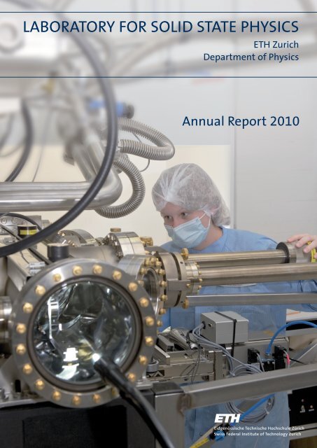
Cover page: Jessica Gmür operating the Molecular Beam Epitaxy system (Wegscheider group)<br />
This annual report was edited by: Philip Moll
PREFACE<br />
The <strong>Laboratory</strong> <strong>for</strong> <strong>Solid</strong> <strong>State</strong> <strong>Physics</strong> at <strong>ETH</strong> Zurich is pleased to present the Annual Report <strong>for</strong> 2010. This report<br />
summarizes our diverse research highlights which have been published in high ranking journals and presented at international<br />
conferences. The members of the <strong>Laboratory</strong> are also committed to all aspects of teaching. Bachelor and<br />
Master level courses were offered <strong>for</strong> physics students as well as <strong>for</strong> students of other departments.<br />
The experimental research at the laboratory of solid state physics and our teaching activities benefit from the excellent<br />
infrastructure provided by <strong>ETH</strong> Zurich and in particular by the physics department. We thank the involved people <strong>for</strong><br />
their dedication and solid support especially in all technical and administrative matters.<br />
Prof. M. Erbudak has been a long time member of our laboratory. He has officially retired in spring 2010. His research<br />
interest focused on the electronic and atomic structure of solid surfaces. Through his course in surface physics he has<br />
inspired many students <strong>for</strong> this research field. His discovery of a novel method to resolve surface structures offered<br />
the possibility to solve numerous open problems regarding the surface structure of novel material classes. We will<br />
miss Prof. Erbudak as a member of the <strong>Laboratory</strong> and as a colleague.<br />
We very gratefully acknowledge the continuous and substantial support by the Schulleitung of <strong>ETH</strong> Zurich, but also<br />
by the Swiss National Science Foundation, the Commission <strong>for</strong> Technology and Innovation (KTI), the European Research<br />
Council, industrial partners and all other sources.<br />
For preparing this Annual Report, we would like to thank Mr. Ph. Moll <strong>for</strong> editing the report and Mrs. Heidi<br />
Hostettler as well as Mrs. Amanda Eisenhut <strong>for</strong> the graphical design.<br />
Zürich, April 2011<br />
Der Vorsteher<br />
Prof. Dr. A. Vaterlaus
Contents<br />
1 <strong>Physics</strong> of New Materials 9<br />
1.1 Electronic mass enhancement in the pnictide superconductor LaRu 2 P 2 studied by quantum oscillations 10<br />
1.2 µSR study of RbFe 2 As 2 . . . . . . . . . . . . . . . . . . . . . . . . . . . . . . . . . . . . . . . . . 11<br />
1.3 Heavy quasi particle mass in (Rb,Cs)Fe 2 As 2 . . . . . . . . . . . . . . . . . . . . . . . . . . . . . . . 11<br />
1.4 Formation of conducting interfaces by charge transfer between two organic crystals . . . . . . . . . . 12<br />
1.5 Organic field-effect transistors on flexible substrates . . . . . . . . . . . . . . . . . . . . . . . . . . . 13<br />
1.6 Impedance Spectroscopy Measurements of Rubrene Single Crystal FETs . . . . . . . . . . . . . . . . 13<br />
1.7 Superconductivity above 50 K in Th-substituted SmFeAsO . . . . . . . . . . . . . . . . . . . . . . . 15<br />
1.8 Superconductivity in SmFe(As,P)O compound . . . . . . . . . . . . . . . . . . . . . . . . . . . . . 16<br />
1.9 SmFe 1−x Co x AsO and NdFeAs(O,F) single crystals from NaAs flux . . . . . . . . . . . . . . . . . . 16<br />
1.10 Studies of superconducting properties of 122-type Fe-based arsenides . . . . . . . . . . . . . . . . . 17<br />
1.11 High pressure liquid epitaxy of (Al,Ga)N thick layers . . . . . . . . . . . . . . . . . . . . . . . . . . 18<br />
1.12 Self-aligned Ge crystals on Si substrates . . . . . . . . . . . . . . . . . . . . . . . . . . . . . . . . . 18<br />
2 <strong>Physics</strong> of Semiconductor Nanostructures 21<br />
2.1 Observation of excited states in a graphene double quantum dot . . . . . . . . . . . . . . . . . . . . . 23<br />
2.2 Quantum capacitance and density of states of graphene . . . . . . . . . . . . . . . . . . . . . . . . . 24<br />
2.3 Gating of high-mobility two-dimensional electron gases in GaAs/AlGaAs<br />
heterostructures . . . . . . . . . . . . . . . . . . . . . . . . . . . . . . . . . . . . . . . . . . . . . . 25<br />
2.4 Suppression of weak antilocalization in InAs nanowires . . . . . . . . . . . . . . . . . . . . . . . . . 26<br />
2.5 Rectification in three-terminal graphene junctions . . . . . . . . . . . . . . . . . . . . . . . . . . . . 27<br />
2.6 Spin <strong>State</strong>s in Graphene Quantum Dots . . . . . . . . . . . . . . . . . . . . . . . . . . . . . . . . . 28<br />
2.7 Evidence <strong>for</strong> localization and 0.7 anomaly in hole quantum point contacts . . . . . . . . . . . . . . . 29<br />
2.8 Highly Tunable Hybrid Quantum Dots with Charge Detection . . . . . . . . . . . . . . . . . . . . . 30<br />
2.9 Imaging Localized <strong>State</strong>s in Graphene Nanostructures . . . . . . . . . . . . . . . . . . . . . . . . . . 31<br />
2.10 An in-situ tunable radio-frequency quantum point contact . . . . . . . . . . . . . . . . . . . . . . . . 32<br />
2.11 Towards electron transport measurements in chemically modified graphene: The effect of a solvent . . 33<br />
2.12 Role of linear and cubic terms <strong>for</strong> drift-induced Dresselhaus spin-orbit splitting in a two-dimensional<br />
electron gas . . . . . . . . . . . . . . . . . . . . . . . . . . . . . . . . . . . . . . . . . . . . . . . . 34
6 Contents<br />
3 Condensed Matter at Low Temperatures 37<br />
3.1 Distribution of magnetic relaxations in a random Heisenberg chain revealed by NMR . . . . . . . . . 38<br />
3.2 High-field NMR investigation of the BiCu 2 PO 6 spin ladder . . . . . . . . . . . . . . . . . . . . . . . 39<br />
3.3 Direct observation of a quasi-one-dimensional magnetic phase . . . . . . . . . . . . . . . . . . . . . 40<br />
4 Magnetism, Electron Spectroscopy 43<br />
4.1 Nanoscale Magnetism . . . . . . . . . . . . . . . . . . . . . . . . . . . . . . . . . . . . . . . . . . . 44<br />
4.1.1 Experimental phase diagram of perpendicularly magnetized ultrathin ferromagnetic films . . . 44<br />
4.2 Surface <strong>Physics</strong> . . . . . . . . . . . . . . . . . . . . . . . . . . . . . . . . . . . . . . . . . . . . . . 45<br />
4.2.1 Faceting of quasicrystal surfaces . . . . . . . . . . . . . . . . . . . . . . . . . . . . . . . . . 45<br />
4.3 Thin Film <strong>Physics</strong> Group . . . . . . . . . . . . . . . . . . . . . . . . . . . . . . . . . . . . . . . . . 47<br />
4.3.1 Continuously Tunable Single Mode VECSEL . . . . . . . . . . . . . . . . . . . . . . . . . . 47<br />
4.3.2 Room Temperature Operation of PbSe QW in a Modular Setup . . . . . . . . . . . . . . . . . 48<br />
4.3.3 PbSrS Double Heterostructures <strong>for</strong> Shorter Wavelengths in a Modular Setup . . . . . . . . . . 49<br />
4.3.4 Ternary PbSnSe <strong>for</strong> Longer Wavelengths . . . . . . . . . . . . . . . . . . . . . . . . . . . . 50<br />
5 Optical Spectroscopy 51<br />
5.1 Temperature dependence of the excitation spectrum in the charge-density-wave ErTe 3 and HoTe 3<br />
systems . . . . . . . . . . . . . . . . . . . . . . . . . . . . . . . . . . . . . . . . . . . . . . . . . . 53<br />
5.2 Charge dynamics of the Co-doped BaFe 2 As 2 . . . . . . . . . . . . . . . . . . . . . . . . . . . . . . 54<br />
6 <strong>Solid</strong>-<strong>State</strong> Dynamics and Education 59<br />
6.1 Ultrafast magnetometry using free electron laser radiation . . . . . . . . . . . . . . . . . . . . . . . . 61<br />
6.2 Single shot magnetic imaging . . . . . . . . . . . . . . . . . . . . . . . . . . . . . . . . . . . . . . . 62<br />
6.3 E-Learning and teaching support . . . . . . . . . . . . . . . . . . . . . . . . . . . . . . . . . . . . . 62<br />
6.4 Filep & Innovedum projects . . . . . . . . . . . . . . . . . . . . . . . . . . . . . . . . . . . . . . . 64<br />
7 Quantum Device Lab 65<br />
7.1 Quantum-To-Classical Transition in Cavity Quantum Electrodynamics . . . . . . . . . . . . . . . . . 67<br />
7.2 Cavity QED with Separate Photon Storage and Qubit Readout Modes . . . . . . . . . . . . . . . . . 68<br />
7.3 Control and Tomography of a Three Level Superconducting Artificial Atom . . . . . . . . . . . . . . 69<br />
7.4 Characterization of a Microwave Resonator via a Nearby Quantum Dot . . . . . . . . . . . . . . . . 70<br />
7.5 Hybrid Cavity Quantum Electrodynamics with Atoms and Circuits . . . . . . . . . . . . . . . . . . . 71<br />
8 Semiconductor Quantum Materials 73<br />
8.1 Molecular beam epitaxy of ultrapure semiconductor heterostructures . . . . . . . . . . . . . . . . . . 75<br />
8.2 Raman spectroscopy at ultra low temperatures . . . . . . . . . . . . . . . . . . . . . . . . . . . . . . 77<br />
8.3 Photons talk to correlated electrons in quantum hall states . . . . . . . . . . . . . . . . . . . . . . . . 78
Contents 7<br />
9 Neutron scattering and magnetism 81<br />
9.1 Phase transitions in magnetically ordered systems . . . . . . . . . . . . . . . . . . . . . . . . . . . . 83<br />
9.1.1 Novel AF-cone phase of an exotic Dzyaloshinskii-Moriya helimagnet . . . . . . . . . . . . 83<br />
9.1.2 Double spin flop transition in a quasi-1D antiferromagnet . . . . . . . . . . . . . . . . . . . 84<br />
9.2 Excitations and scaling in quantum magnets . . . . . . . . . . . . . . . . . . . . . . . . . . . . . . 84<br />
9.2.1 Field dependence of the Luttinger parameter in a Heisenberg spin chain . . . . . . . . . . . 84<br />
9.2.2 Finite-T effects in a quantum spin ladder . . . . . . . . . . . . . . . . . . . . . . . . . . . . 85<br />
9.2.3 An almost-perfect strong-leg quantum spin ladder . . . . . . . . . . . . . . . . . . . . . . . 86<br />
9.3 Static disorder in quantum magnets . . . . . . . . . . . . . . . . . . . . . . . . . . . . . . . . . . . 87<br />
9.3.1 Quenched disorder in a quasi-2D quantum spin liquid . . . . . . . . . . . . . . . . . . . . . 87<br />
9.3.2 Random field state in a disordered frustrated quantum spin ladder . . . . . . . . . . . . . . . 88<br />
9.3.3 Effect of bond disorder on weakly-coupled spin-1/2 chains . . . . . . . . . . . . . . . . . . . 88<br />
9.4 Ferroelectric materials . . . . . . . . . . . . . . . . . . . . . . . . . . . . . . . . . . . . . . . . . . 89<br />
10 Publications 91<br />
11 Presentations 105
Chapter 1<br />
<strong>Physics</strong> of New Materials<br />
Head<br />
Prof. Dr. Bertram Batlogg<br />
(http://www.pnm.ethz.ch/)<br />
Academic Staff<br />
Dr. Claudiu Falub Jonathan Hanselmann Roger Häusermann<br />
Wolfgang Kalb Jakob Kanter Thomas Mathis<br />
Philip Moll Tobias Morf PD Dr. Hans von Känel<br />
Tino Zimmerling<br />
Technical Staff<br />
Kurt Mattenberger<br />
Administrative Staff<br />
Gabriela Strahm<br />
Master Theses<br />
Kristin Leidel HS 2010<br />
PhD Theses<br />
Andrey Belousov FS 2010<br />
Florian Pfuner HS 2010<br />
High Pressure Synthesis<br />
Head<br />
Dr. Janusz Karpinski<br />
Academic Staff<br />
Andrey Belousov Dr. Zbigniew Bukowski Dr. Sergiy Katrych<br />
Dr. Nikolai Zhigadlo<br />
Academic Guests<br />
Dr. Roman Puzniak, Polish Academy of Sciences, Warsaw(Poland)<br />
Dr. Krzysztof Rogacki, Polish Academy of Sciences, Wroclaw(Poland)
10 <strong>Physics</strong> of New Materials<br />
1.1 Electronic mass enhancement in the pnictide superconductor LaRu 2 P 2 studied<br />
by quantum oscillations<br />
P.J.W. Moll, J. Kanter, Z. Bukowski, J. Karpinski, B. Batlogg, in collaboration with R.D. McDonald, F. Balakirev (NHMFL / Los Alamos, USA), P. Blaha, K.-H.<br />
Schwarz (TU Vienna, Austria)<br />
As the iron-pnictides constitute a new class of unconventional high-temperature superconductors besides the cuprates,<br />
the importance of electronic correlations as a key ingredient <strong>for</strong> superconductivity needs to be adressed in these systems.<br />
The ruthenate LaRu 2 P 2 is a low temperature superconductor (T c ≈ 4K), isostructural to the 38K superconductor<br />
(Ba,K)Fe 2 As 2 . However, its iron-based relative LaFe 2 P 2 is non-superconducting, despite being at first sight more<br />
closely related to the Fe-3d high T c iron-pnictides. To probe the electronic structure of LaRu 2 P 2 , we have studied<br />
the oscillatory behavior of the magnetization due to the quantization of electronic orbits in increasing magnetic field<br />
- known as the de Haas-van Alphen effect (Fig. 1.1a). As a result of this quantum mechanical effect, the frequency<br />
of this oscillation is proportional to the extremal cross-sections of the Fermi surface (FS) perpendicular to the applied<br />
magnetic field. The dHvA-effect is a most powerful tool to investigate the bulk Fermi surface of a metal tomographically,<br />
as well as to determine its differential properties such as the effective electronic mass. As the angle between<br />
field and sample is changed, the frequencies shift according to the shape of the FS (Fig.1.2a). In Fig.1.1b, we find<br />
excellent agreement between the measured (left) and calculated (right) frequencies. The DFT band structure calculations<br />
(WIEN2k) thus reproduce the electronic structure of LaRu 2 P 2 at the Fermi level very well. The FS of LaRu 2 P 2<br />
and LaFe 2 P 2 are quite similar (Fig.1.2a), in particular the electron cylinder at the zone edge is a robust feature of all<br />
tetragonal ”122” pnictides. We have extracted the effective electron mass m ∗ = 0.99m e (m e : free electron mass)<br />
from the temperature dependence of the dHvA amplitudes. The band structure calculations predict an effective mass<br />
m b of 0.55 m e , resulting in a strong mass renormalization λ = m∗<br />
m b<br />
− 1 = 0.8.<br />
Figure 1.1: a) Raw magnetic torque of LaRu 2P 2 at various temperatures.<br />
The oscillatory behavior is clearly visible at the high<br />
temperature of 20K, indicative of the low effective masses. b)<br />
Measured (left) and calculated (right) angular dependence of the<br />
dHvA frequencies agree very well: This shows that DFT calculations<br />
accurately describe the electronic structure.<br />
Figure 1.2: a) Fermi surfaces of LaFe 2P 2 and LaRu 2P 2 calculated<br />
using the DFT code WIEN2k. b) Electronic density of<br />
states (DOS) of both materials. The more delocalized Ru4d orbitals<br />
give rise to the broader bandwidth in the Ru compound.
1.2. µSR study of RbFe 2 As 2 11<br />
1.2 Muon-Spin-Rotation study of the superconducting state of RbFe 2 As 2<br />
J. Kanter, Z. Bukowski, J. Karpinski & B. Batlogg<br />
in collaboration with: Z. Shermadini, C. Baines, M. Bendele, R. Khasanov, H.-H. Klauss, H. Luetkens, H. Maeter,<br />
G. Pascua & A. Amato at PSI Villigen<br />
RbFe 2 As 2 is a member of the iron-arsenide 122 family and was only recently synthesized and found to be superconducting<br />
below 2.6 K in our research group by Bukowski et al. Compared to the related BaFe 2 As 2 , RbFe 2 As 2 does not<br />
order magnetically and possesses a lower Fermi level.<br />
To investigate the superconducting state, Muon Spin Rotation (µSR) measurements have been per<strong>for</strong>med at the Paul<br />
Scherrer Institute (PSI) in Villigen. µSR as a local probe of the internal magnetic fields is able to probe the magnetic<br />
penetration depth λ and thus the superconducting carrier concentration n s ∝ 1/λ 2 . Fits to the temperature dependence<br />
of λ are in agreement with a two gap model <strong>for</strong> the superconducting phase, with gaps of ∆ 1 = 0.15(2) meV,<br />
∆ 2 = 0.49(4) meV. The temperature dependence of the upper critical field B c2 as deduced from µSR data is in good<br />
agreement with the transport data measured in our laboratory.<br />
Figure 1.3: left: The fit to the temperature dependence of the magnetic penetration depth λ(T ) is in agreement with a two gap s + s model.<br />
middle: Low temperature resistivity data <strong>for</strong> different magnetic fields to deduce the upper critical field B c2. right: Temperature dependence<br />
of the upper critical field B c2 obtained from temperature (full diamonds) and field dependence (open circles) of the spin depolarisation factor<br />
σ s and the resistivity data (blue stars). The solid line is a guide to the eye. Figure credit: Z. Shermadini et al., PRB 82, 144527 (2010)<br />
1.3 Heavy quasi particle mass in (Rb,Cs)Fe 2 As 2<br />
J. Kanter, Z. Bukowski, J. Karpinski & B. Batlogg, in collabration with S. Griffin, Materials Theory Group, <strong>ETH</strong> Zuerich<br />
Iron-based superconductors, discovered in 2007, have attracted considerable attention in the last three years as they<br />
might help to understand the underlying mechanisms of high temperature superconductivity. RbFe 2 As 2 , a member<br />
of the iron-arsenide 122 family, has recently been synthesized and found to be superconducting below 2.6 K in our<br />
research group. Compared to the related BaFe 2 As 2 the electron density is lower and no magnetic order is observed.<br />
Interestingly, we found the electronic contribution γ to the specific heat to be about 112 mJ/mole/K 2 , which is about<br />
two to three times higher than <strong>for</strong> comparable 122 compounds. An even higher γ-coefficient of 178 mJ/mole/K 2 is<br />
measured when Cs is substituted <strong>for</strong> Rb, which leads to a suppression of superconductivity.<br />
To investigate the origin of the high electronic specific heat band structure calculations have been per<strong>for</strong>med using<br />
GGA+U calculations as implemented in the VASP code. These calculations reveal flat hybridized Fe-d bands around<br />
the Γ and M point. The resulting peak of the density of states at the Fermi level would explain the high values of<br />
γ. Quantum oscillation measurements, such as Shubnikow-de-Haas or de-Haas-van-Alphen measurements should be<br />
per<strong>for</strong>med on single crystals to verify the calculations of the Fermi surface.
12 <strong>Physics</strong> of New Materials<br />
Figure 1.4: left: Specific heat measurements of Rb xCs 1−xFe 2As 2 samples with increasing Cs content from black to orange (x=1, 0.67, 0.33,<br />
0). The value of the fit at T = 0 K indicates the high quasi particle mass. right: Band structure calculations show flat non-dispersive Fe-d bands<br />
close to the Fermi surface, which might explain the enhanced quasi particle mass.<br />
1.4 Formation of conducting interfaces by charge transfer between two organic<br />
crystals<br />
Thomas Mathis, Fabian Menges, Kurt Mattenberger, Bertram Batlogg<br />
By laminating two organic crystals their interface can become conducting due to charge transfer across the interface.<br />
Ideally this interface would be <strong>for</strong>med by epitaxial growth of one crystal on top of the other. To understand the<br />
<strong>for</strong>mation of the conductive interface between TTF and TCNQ we have studied the electrical conductivity as a function<br />
of time. Electrodes were directly deposited onto the TCNQ crystal to make sure the electrodes are right at the interface<br />
and have a clearly defined geometry. Then the TTF crystal was laminated on top of the TCNQ crystal, and the<br />
conductivity increase was measured as function of time after a TTF crystal was placed on top of a TCNQ crystal, as<br />
shown in the left picture in figure 1.6.<br />
Figure 1.5: Evolution with time of the interface conductivity between TTF and TCNQ crystals. Comparing RT laminated and cold laminated<br />
interfaces shows that at low temperature the conductivity increase can be slowed down drastically. The right graph with the logarithmic sheet<br />
conductivity also illustrates the different behavior of the sheet conductivity evolution at different temperature ramping curves. The starting<br />
temperature was 250K <strong>for</strong> both but then the increase in temperature was different, even cooling back down and reheating was involved.<br />
This lamination step has been started either at room temperature or at 250K. At RT, the conductivity increases rapidly<br />
over several orders of magnitude within 50 minutes, yet not instantaneously as could be expected from charge transfer<br />
across two ideally flat surfaces. As the conductivity increases <strong>for</strong> hours and days, and TTF is known to sublime at RT,<br />
we conclude that TTF molecules attach onto the TCNQ crystal by sublimation and perhaps some surface diffusion.<br />
This is confirmed by the much slower conductivity increase when measured at low temperatures. In figure 1.5 two
1.5. Organic field-effect transistors on flexible substrates 13<br />
Figure 1.6: TTF crystal lamination on a TCNQ crystal. Left: Typical arrangement of a TCNQ crystal with gold electrodes, covered by a TTF<br />
crystal. Right: After the main TTF crystal is removed, the presence of remaining TTF is mapped via the sulfur signature in EDX. In a scan<br />
along the red line, TTF is found outside the contact area (arrows), deposited by sublimation.<br />
examples are shown. In addition the build-up of TTF molecules away from the immediate contact area has been<br />
confirmed by measuring the sulfur concentration profile using EDX. The saturation conductivity reaches typically a<br />
value of 5x10 −5 Siemens square, close to, but slightly less than the value expected <strong>for</strong> a fully metallic interface.<br />
1.5 Organic field-effect transistors on flexible substrates<br />
T. Morf, L. Talirz, B. Batlogg<br />
One of the key advantages of organic semiconductors is their<br />
mechanical flexibility which gives rise to a wealth of possible<br />
new applications. It is thus important to understand the intrinsic<br />
behavior of used materials under mechanical stress. Apart from<br />
the ultimate load be<strong>for</strong>e breaking, this includes per<strong>for</strong>mance in<br />
the bent state and degradation with repeated bending cycles.<br />
Various materials are investigated by measurements on field-effect<br />
transistors. This includes — apart from the semiconductor —<br />
electrodes and the gate dielectric. By means of their different<br />
Young’s moduli and the device geometry, each layer is contributes<br />
to the total strain in the active region.<br />
Figure 1.7: A sample produced on a flexible Kapton substrate<br />
in the home-made bending tool.<br />
crucial <strong>for</strong> the per<strong>for</strong>mance of devices. Ongoing research aims at<br />
Preliminary results indicate that the gate insulator is particularly<br />
optimizing the dielectric layer <strong>for</strong> both electrical and mechanical<br />
per<strong>for</strong>mance. This will allow the investigation of processes in the semiconductor under tensile and compressive strain.<br />
1.6 Impedance Spectroscopy Measurements of Rubrene Single Crystal FETs<br />
T. Kreiliger, T. Zimmerling and B. Batlogg<br />
The goal of this project is to analyze time-dependent phenomena in organic semiconductors by impedance spectroscopy<br />
measurements. In devices based on organic semiconductors trapping and detrapping of charge carriers by
semiconductor.010200210300310400410<br />
200 210 300 310 40056789<br />
14 <strong>Physics</strong> of New Materials<br />
in-gap states of the semiconductor is assumed to occur at different time constants. There<strong>for</strong>e, frequency-dependent<br />
conductivity measurements might give us an insight in the time-dependent microscopic trapping processes involved<br />
in these materials.<br />
The field-effect transistor (FET) structure employed in these experiments is shown in the inset of Figure 1.8. Rubrene<br />
single crystals were grown by means of physical vapor transport. A constant gate voltage (V g ) and an alternating<br />
source-to-drain voltage (V ac ) was applied while measuring the resulting source-to-drain current. The measurements<br />
were conducted under ultra high vacuum conditions and at temperatures ranging from 300 K down to 150 K. An<br />
excellent shielding of the cables and Rubrene single crystals with low trap density allowed us to per<strong>for</strong>m reliable<br />
measurements in a wide frequency range from usually 100 Hz to 10 MHz. Given these experimental conditions,<br />
we were able to investigate time-dependent processes while shifting the Fermi level towards the band edge of the<br />
789<br />
Figure 1.8: An example impedance measurement of a Rubrene single crystal FET at 300 K<br />
An example of our measurements is shown in a Cole-Cole plot in Figure 1.8. For low frequencies, the device behaves<br />
like a simple resistor. For higher frequencies, however, the charge carries can no longer be trapped and released fast<br />
enough to follow the ac voltage and the impedance <strong>for</strong>ms a semi circle in the complex plane. This is typical <strong>for</strong> a<br />
resistor and a capacitor in parallel.
1.7. Superconductivity above 50 K in Th-substituted SmFeAsO 15<br />
1.7 Superconductivity above 50 K in Th-substituted SmFeAsO<br />
N.D. Zhigadlo, S. Katrych, Z. Bukowski, J. Fidelus, J. Karpinski in collaboration with P. Moll, B. Batlogg, R. Khasanov, S. Weyeneth, H. Keller<br />
Sm 1−x Th x FeAsO poly- and single-crystalline samples with partial substitution of Sm 3+ by Th 4+ with a sharp diamagnetic<br />
onset at T c up to 53 K were synthesized using high pressure technique. The T c depends on the Th and F<br />
substitution as shown in Fig.1.9.<br />
Figure 1.9: T c dependence on doping by Th and F substitutions<br />
in SmFeAsO.<br />
Both Th and F cause similar variation of T c . The unit-cell parameters<br />
a and c shrink with Th substitution and the fractional atomic<br />
coordinate of the As site z(As) remains almost unchanged, while<br />
that of Sm/Th increases. The As-Sm/Th distance shortens and the<br />
O-Sm/Th distance elongates. Equivalently one may focus on the<br />
”layers” of the structure: the Sm/ThO layer expands (∆ s1 =0.055<br />
Å), the AsFe layer remains unaffected, and the distance S 3 between<br />
the Sm/ThO and the AsFe layers shortens by ∆ s3 =0.048<br />
Å(Fig. 1.10a). Bulk superconducting samples do not undergo a<br />
structural phase transition from tetragonal to orthorhombic symmetry<br />
at low temperatures. Upon warming from 5 to 295 K the<br />
increase in the FeAs layer thickness is dominant (Fig. 1.10b,c),<br />
while the changes in the other structural building blocks are minor,<br />
and they compensate each other, since the As-Sm/Th distance<br />
contracts by about the same amount as the O-Sm/Th expands.<br />
Figure 1.10: (a) Schematic representation of the projection of Sm 1−xTh xFeAsO lattice fragments on the ac plane and the changes in its<br />
dimensions (red dotted lines) with substitution of Sm by Th. (b) Schematic representation of the thermal expansion of FeAs 4 tetrahedron <strong>for</strong><br />
Sm 0.90(5) Th 0.10(5) FeAsO at 15 K (solid lines and circles) and 295 K (dotted lines and circles). (c) Pnictogen height (h P n) as a function of<br />
temperature <strong>for</strong> the three Sm 1−xTh xFeAsO compositions.
16 <strong>Physics</strong> of New Materials<br />
1.8 Superconductivity in SmFe(As,P)O compound<br />
N.D. Zhigadlo, S. Katrych, Z. Bukowski, J. Fidelus, J. Karpinski in collaboration with P. Moll, B. Batlogg, R. Khasanov, S. Weyeneth, H. Keller<br />
Polycrystalline and single-crystalline samples of SmFeAs 1−x P x O were successfully prepared in a quartz ampoule<br />
and in the high-pressure cubic anvil. In samples prepared at ambient pressure substitution of As by P results in decrease<br />
of the unit-cell volume and continuous suppression of both the ordering temperatures. Superconductivity in the<br />
SmFeAs 1−x P x O 1−y samples caused by oxygen deficiency appears only after heat treatment under high pressure. The<br />
pressure-induced oxygen deficiency brings the Sm-O charge-transfer layer closer to the superconducting As-Fe-As<br />
block and facilitates electron transfer. Muon spin rotation studies show, that <strong>for</strong> superconducting SmFeAs 0.5 P 0.5 O 1−y<br />
samples only dynamic magnetism survived, while the ambient prepared samples with the same amount of P substitution<br />
still show a static magnetic moment at temperatures below 60 K. Point-contact Andreev-reflection spectroscopy<br />
indicates the existence of two energy gaps in superconducting samples supporting a common multigap scenario proposed<br />
<strong>for</strong> FeAs-based superconductors. Single crystals of SmFeAs 1−x P x O 1−y have been grown under high pressure.<br />
Figure 1.11: (a) Temperature dependence of the magnetoresistance <strong>for</strong> crystals of SmFeAs 0.5P 0.5O 0.85 (nominal composition).<br />
Left and right insets show measurements with the field applied parallel to the Fe 2As/P 2 layers (H||ab) and perpendicular to them<br />
(H||c), in various magnetic fields (0-14 T, 2 T steps). (b) Temperature dependence of the upper critical field with H||ab and H||c.<br />
To determine H c2 the 50% -ρ n criterion was used.<br />
Magnetoresistance measurements ρ(T,H) near T c <strong>for</strong> magnetic fields parallel (H||ab) and perpendicular (H||c) to<br />
the FeAs/P-planes show remarkably different behavior than that of Sm1111 substituted with F <strong>for</strong> O or Th <strong>for</strong> Sm<br />
(Fig.1.11). In these cases the magnetic fields cause only a slight shift of the onset of superconductivity, but a significant<br />
broadening of the transition, indicating weak pinning and accordingly large flux flow dissipation. In P substituted<br />
Sm1111 crystals the presence of magnetic fields shift the onset of superconductivity to lower temperatures, without a<br />
significant broadening of the transition. The upper critical field deduced from resistance measurements is anisotropic<br />
with slopes of 5.7 T/K (H||ab plane) and 1.3 T/K (H||c axis) sufficiently far below T c .<br />
1.9 SmFe 1−x Co x AsO and NdFeAs(O,F) single crystals from NaAs flux<br />
N.D. Zhigadlo, S. Katrych, Z. Bukowski, J. Karpinski<br />
In order to increase the size and surface quality of LnFeAsO single crystals different kinds of fluxes were investigated.<br />
By using NaAs and KAs fluxes SmFe 1−x Co x AsO and NdFeAs(O,F) crystals of a size up to 0.7 mm have been grown.<br />
Magnetization measurements show relatively sharp superconducting transitions with maximum T c of 16 and 39 K<br />
respectively (Fig. 1.12a). Fig. 1.12b shows NdFeAs(O,F) crystals.
1.10. Studies of superconducting properties of 122-type Fe-based arsenides 17<br />
Figure 1.12: (a) Single crystals of NdFeAs(O,F) on mm scale. (b)<br />
Magnetic signature of the superconducting transition.<br />
1.10 Studies of superconducting properties of 122-type Fe-based arsenides<br />
N.D. Zhigadlo, S. Katrych, Z. Bukowski, J. Fidelus, J. Karpinski, P. Moll, B. Batlogg, in collaboration with R. Khasanov, S. Weyeneth, H. Keller<br />
Polycrystalline samples of the Ba 1−x Rb x Fe 2 As 2 system were synthesized in quartz ampoules with 0
18 <strong>Physics</strong> of New Materials<br />
single crystal shows anomalous field dependence (Fig. 1.14). Below 5 K, zero resistance and a field induced transition<br />
to normal state are observed. In the temperature range 5-7 K with increasing fields the resistance shows a maximum (≈<br />
1000 Oe) then drops to zero and finally the transition to normal state is observed. At present the detailed understanding<br />
of this anomalous magnetoresistance is emerging, and it is, most likely, connected to the effect of field induced Eu-spin<br />
reorientation on the vortex pinning.<br />
1.11 High pressure liquid epitaxy of (Al,Ga)N thick layers<br />
J. Fidelus, S. Katrych, Z. Bukowski, J. Karpinski<br />
A series of experiments of (Al,Ga)N thick layers growth on AlN wafers from solution in Ga have been per<strong>for</strong>med. The<br />
growth of the layers at substrate temperatures 1630-1700 ◦ C with temperature gradients of 10-20 ◦ C/cm at nitrogen<br />
pressure of 7-10 kbar was studied. The precursor, a high pressure synthesized polycrystalline Al y Ga 1−y N pellet,<br />
serving as a source of the feed material was placed in the higher temperature zone of the high pressure furnace in a BN<br />
crucible. The goal was to obtain continuous epitaxial layers with various compositions. The experiments resulted in<br />
thick (up to about 200 µm) structurally oriented layers of Al x Ga 1−x N with Al content 0.8¡x¡0.9. The crystallographic<br />
orientation of the layers is the same as the AlN substrate. The composition and morphology of such layers strongly<br />
depends on the process pressure, temperature range, temperature gradient and nitrogen super-saturation.<br />
Figure 1.15: Thick epitaxial (A,Ga)N layers on AlN substrates grown<br />
at high N 2 pressure (p=8-10 kbar) at T=1630-1700 ◦ C. a) View from<br />
top revealing the growth steps, b) side view of 100 µ m thick layer<br />
(darker), c) SEM picture with material contrast of a 20 µ m thick layer<br />
(lighter) on AlN substrate (darker), d) X-ray diffraction showing the<br />
same orientation of (Al,Ga)N layer and AlN substrate.<br />
1.12 Self-aligned Ge crystals on Si substrates<br />
C.V. Falub, E. Müller, and H. von Känel<br />
In collaboration with: F. Isa, D. Chrastina, G. Isella (L-NESS, Politecnico di Milano, Italy), R. Bergamaschini, A. Marzegalli, L. Miglio (Dip. Di Scienza dei<br />
Materiali, Univ. di Milano-Bicocca, Italy), P. Niedermann, A. Neels, A. Dommann (Centre Suisse d’Electronique et Microtechnique, Switzerland)<br />
Integration of optoelectronic and photonic devices with Si microelectronics technology has been a long-standing goal<br />
and an active research area <strong>for</strong> many years. Yet, the key challenge is the integration of crystalline materials with<br />
dissimilar lattice parameters and thermal properties on top of each other. In the case of heteroepitaxy of Ge on Si<br />
substrates, where the lattice mismatch is 4%, the growth of continuous films suffers from the excessive threading
1.12. Self-aligned Ge crystals on Si substrates 19<br />
dislocation (TD) density. In view of the mismatch of the thermal expansion coefficients, additional problems occur<br />
with increasing layer thickness, such as wafer bowing and crack <strong>for</strong>mation after the epitaxial growth.<br />
By using dedicated patterned Si substrates, fabricated by standard lithography and deep reactive ion etching, and by<br />
tuning the deposition parameters (e.g. substrate temperature, growth rate) in a low energy plasma enhanced chemical<br />
vapor deposition (LEPECVD) chamber, one can tweak the ratio between the lateral and vertical growth velocities,<br />
such that epitaxial growth is limited to small, well defined substrate areas, on which the Ge grows in the <strong>for</strong>m of<br />
isolated self-aligned crystals, i.e. pillars. The basic idea behind our new approach is there<strong>for</strong>e to avoid a continuous<br />
layer to <strong>for</strong>m during the growth. The analysis of such structures by scanning and transmission electron microscopy,<br />
atomic <strong>for</strong>ce microscopy and high-resolution X-ray diffraction revealed that a fundamental breakthrough had been<br />
achieved. Each pillar consists of a nearly perfect single crystal with well-defined facets. The TDs, usually degrading<br />
the electrical properties of heteroepitaxial layer stacks are confined to a narrow region close to the interface with the<br />
Si-substrate. No cracks can <strong>for</strong>m as long as adjacent pillars remain separated, and wafer bowing is virtually absent.<br />
As a next step we intend to apply these structures to high-resolution CMOS based x-ray pixel detectors.<br />
Figure 1.16: a) SEM micrograph of 8 µm high Ge crystals grown epitaxially on patterned Si substrates; the inset shows the top SEM<br />
micrograph of one of the Ge crystals. b) High-resolution θ − 2θ scans <strong>for</strong> a Ge wafer and a 20 µm thick epilayer consisting of self-aligned Ge<br />
crystals. c) and d) High-resolution reciprocal space maps measured around the Ge(004) reflection <strong>for</strong> a 20 µm thick epilayer of Ge crystals and<br />
a 20 µm thick epilayer.
Chapter 2<br />
<strong>Physics</strong> of Semiconductor Nanostructures<br />
Head<br />
Prof. Dr. K. Ensslin<br />
Prof. Dr. T. Ihn<br />
Prof. Dr. R. Monnier<br />
(http://www.nanophys.ethz.ch)<br />
Academic Staff<br />
T. Müller J. Güttinger F. Molitor<br />
S. Baer S. Hellmüller F. Nichele<br />
D. Bischoff M. Hüfner N. Pascher<br />
T. Choi A. Jacobsen Dr. C. Rössler<br />
Dr. M. Csontos Y. Komijani Dr. P. Roulleau<br />
S. Dröscher B. Küng S. Schnez<br />
T. Frey Dr. P. Leek M. Studer<br />
U. Gasser<br />
Technical Staff<br />
C. Barengo P. Studerus<br />
Academic Guests<br />
T. Noguchi, University of Tokyo (2.11.2009-31.1.2010)<br />
K. Shibata, University of Tokyo (27.8.-31.12.2010)<br />
Administrative Staff<br />
C. Egli C. Vinzens<br />
NCCR QSIT Office<br />
Dr. I. Blatter<br />
S. Küenzel
2.1. Observation of excited states in a graphene double quantum dot 23<br />
2.1 Observation of excited states in a graphene double quantum dot<br />
F. Molitor, H. Knowles, S. Dröscher, U. Gasser, T. Choi, P. Roulleau, J. Güttinger, A. Jacobsen, C. Stampfer, K. Ensslin and T. Ihn<br />
Double-quantum-dot structures are promising candidates <strong>for</strong> the implementation of solid-state spin qubits. Double<br />
dots have been realized in many different material systems, as <strong>for</strong> example in GaAs heterostructures, semiconductor<br />
nanowires and carbon nanotubes, and the control of individual electrons and spins has been achieved. Graphene<br />
has been predicted to be particularly well-suited <strong>for</strong> spin-based quantum in<strong>for</strong>mation processing, since spin-orbit<br />
interaction and hyperfine interaction are expected to be much weaker than in the material systems mentioned above.<br />
This property potentially leads to much longer spin coherence times. Significant progress has been made recently in<br />
the fabrication and the understanding of graphene-based nanostructures, as <strong>for</strong> example constrictions and quantum<br />
dots. Also graphene double quantum dots have been demonstrated recently.<br />
sample schematic<br />
experiment<br />
!"#$ !%#$<br />
simulation<br />
Figure 2.1: (a) Schematic representation of the graphene double quantum dot. The two dots are separated by a 30 nm wide constriction and<br />
connected to source and drain (in red) by 20 nm wide constrictions. Two additional constrictions, in blue and green serve as side gates to<br />
control the electrochemical potential of the quantum dots and also as charge detectors <strong>for</strong> the QDs. Additional side gates are shaded in grey.<br />
(b) Measurement of a charge stability diagram around one pair of triple points at small bias volt-age V bias = 15 µ V (c) Simulation of a pair<br />
of triple points <strong>for</strong> an interdot tunneling coupling t = 14 µeV , and the energy independent part of the tunneling rates to the leads γ L = 1.26<br />
GHz and γ R = 1.69 GHz<br />
Figure 2.1(a) shows the schematic of a graphene double dot device. The sample has been patterned from an exfoliated<br />
graphene flake. Graphene has been removed in the grey areas. Current flows from source (S) to drain (D) through the<br />
double dot device. The charge occupancy of the dot as well as the tunneling coupling of the dot to source and drain<br />
and between the dots is tuned by voltages applied to the in-plane gates marked respectively.<br />
Figure 2.1(b) shows a measurement <strong>for</strong> a charge stability diagram in the vicinity of one pair of triple points. It has<br />
been recorded at low temperature (T = 120 mK) and at low bias voltage (V bias = 15 µV) to prevent an expansion<br />
of the triple points to triangles. The interdot tunneling coupling is expected to cause rounded edges of the hexagons,<br />
with the point of charge balance shifted from the original triple point with a distance proportional to the strength of<br />
the tunneling coupling. No rounding of the corners is visible in the measurement presented here with a distance. This<br />
allows us to estimate an upper bound <strong>for</strong> the tunneling coupling t ≤ 20 µeV. This energy scale is comparable to the<br />
temperature broadening of the cotunneling lines (k B T = 10 µeV) and about two orders of magnitude smaller than the<br />
capacitive coupling energy (E C ≈ 1.3 meV). Figure 2.1 (c) shows the result of a numerical calculation of the current<br />
based on a rate equation using the lever arms and charging energies deduced from the measurement. Measurement and<br />
simulation are quite similar, except <strong>for</strong> the finite current measured along the line connecting both triple points, which<br />
is unexpected and can not be reproduced with this simple model. Despite the strong capacitive coupling between both<br />
dots, the tunneling coupling is below the experimental resolution and no rounding of the hexagons at the triple points<br />
can be resolved.<br />
The situation in the graphene constrictions defining the dot barriers is probably much more complicated than in the<br />
case of standard semiconductor quantum dots, where the barriers can be considered as simple tunnel barriers. It is<br />
known from earlier measurements that current through a graphene constriction is suppressed <strong>for</strong> a certain back gate<br />
voltage range due to the <strong>for</strong>mation of localized states in the constriction. This would lead to a complicated system,
24 <strong>Physics</strong> of Semiconductor Nanostructures<br />
where not only the two dots can be charged, but also the localized states in the constrictions. However, because of<br />
the sample geometry the extent of the localized states in the constrictions has to be much smaller than the dot size,<br />
and their charging energies are much larger. This notion is supported by the almost perfect hexagons in the charge<br />
stability diagram despite the possible parasitic dots in the constrictions.<br />
For finite bias applied across the double dot, each of the triple points develops into a triangle whose baseline length<br />
and height is proportional to the bias voltage. Inside the finite-bias triangles, additional structures can be observed,<br />
which we attribute to excited dot states, but partly also to imperfections in the tunnel barriers. With the application of<br />
an in-plane magnetic field, additional states become visible within the finite-bias triangles.<br />
2.2 Quantum capacitance and density of states of graphene<br />
S. Dröscher, P. Roulleau, F. Molitor, P. Studerus, C. Stampfer, K. Ensslin, and T. Ihn<br />
The density of states of a given quantum system is important <strong>for</strong> understanding the electrical conductivity and other<br />
electronic response functions. Direct measurements of the density of states via the quantum capacitance have been<br />
successfully used, <strong>for</strong> example, on semiconductor samples containing a two-dimensional electron gas and carbon nanotubes.<br />
Graphene sheets have been subjected to theoretical studies of the quantum capacitance and first measurements<br />
have been carried out recently. Techniques such as scanning tunneling microscopy were applied to probe the local<br />
density of states of graphene as well. We present experiments on a structure covered with a top gate and interpret our<br />
results based on the presence of disorder in the graphene device.<br />
!"#$<br />
!&#$<br />
!%#$<br />
C tot<br />
Figure 2.2: (a) AFM image of the device studied. The electrodes are colored corresponding to the scheme in (b). (b) Schematic cross section<br />
of a top gated graphene sample. The graphene flake is contacted with gold electrodes and covered partly by an alumina/gold top gate. (c)<br />
Density of states as a function of Fermi energy. The black solid lines show the experimental data assuming different C g from outermost to<br />
inner- most curve: 4.8, 5.8, and 6.8 fF/µm 2 . Error bars are indicated and the theoretically expected density of states <strong>for</strong> a perfectly clean<br />
graphene sheet is drawn as the dashed line.<br />
The samples were fabricated using mechanical exfoliation of graphite powder and subsequent deposition onto 285 nm<br />
SiO 2 on silicon substrate (see Fig. 2.2 (a)). We used an undoped silicon substrate to minimize any parasitic capacitances.<br />
It was verified that the investigated layers consisted of a single atomic sheet using optical microscopy, atomic<br />
<strong>for</strong>ce microscopy as well as Raman spectroscopy. Ohmic contacts were patterned with electron beam lithography
2.3. Gating of high-mobility two-dimensional electron gases in GaAs/AlGaAs<br />
heterostructures 25<br />
followed by metal evaporation of Cr/Au (2 nm/40 nm). In a second electron beam lithography step a mask <strong>for</strong> reactive<br />
ion etching was defined to structure the graphene sheet. The patterned top gate consisted of Ti and Au evaporated<br />
onto an Al 2 O 3 dielectric. An AFM image of the device and a scheme of the cross section are shown in Figs. 2.2 (a)<br />
and (b).<br />
The capacitance of the device was measured using a high-frequency resonant circuit. The resonance frequency was<br />
converted to a capacitance which was evaluated in terms of the density of states of the graphene layer. A careful<br />
analysis of the data leads to the density of states D(E F ) plotted in Fig. 2.2 (c) <strong>for</strong> different gate capacitances C g<br />
between 4.8 and 6.8 fF/µm 2 . This result shows a flat bottom in the energy interval E F = ±50 meV at about 1 ×10 17<br />
eV −1 m 2 with the tendency to increase outside this interval. Error bars indicating the full width at half maximum of<br />
the underlying probability density function <strong>for</strong> D(E F ) are shown <strong>for</strong> selected data points. The dashed line in Fig. 2.2<br />
(c) shows the theoretical density of states of ideal graphene. The deviation between the theoretically expected density<br />
of states and the measured results are attributed to the disorder potential in graphene. The magnitude of the disorder<br />
potential of the device was determined to be of the order of a few 100 meV which is in good agreement with results<br />
obtained in other studies.<br />
2.3 Gating of high-mobility two-dimensional electron gases in GaAs/AlGaAs<br />
heterostructures<br />
C. Rössler, T. Feil, P. Mensch, T. Ihn, K. Ensslin, D. Schuh, and W. Wegscheider<br />
Two-dimensional electron gases (2DEGs) in AlGaAs heterostructures can reach mobilities exceeding<br />
10 7 cm 2 V −1 s − 1 at low temperatures, facilitating the observation of fascinating phenomena like the microwave-induced<br />
zero-resistance states, the ν= 5/2 quantum Hall state and interactions between composite fermions. To study them,<br />
clean materials and other growth techniques beyond the standard modulation doping approach are essential. However,<br />
current growth protocols are apparently in conflict with the in situ control of the 2DEG’s density via Schottky<br />
gates: recent experiments on gated high-mobility structures have reported hysteresis effects and temporal drifts when<br />
biasing Schottky gates. In order to investigate the origin of these effects, we fabricate gated Hall bars containing a<br />
high-mobility 2DEG.<br />
In the investigated samples, the 2DEG resides in a 30 nm wide GaAs quantum well, 160 nm beneath the surface.<br />
Two Si donor layers are situated at depths z of about 40 and 680 nm in order to compensate <strong>for</strong> surface states and<br />
background impurities in the substrate. Since these donors are embedded in AlGaAs, they are expected to <strong>for</strong>m DXcenters<br />
below the Γ-band. Layers of GaAs at z ≈ 70nm and z ≈ 250nm are δ-Si doped and enclosed in 2nm thick<br />
layers of AlAs. The ground state in the AlAs wells (X-minima) is lower than that in the GaAs wells (Γ-minima).<br />
Consequently, only a part of the donorsï¿ 1 2<br />
free electrons reside in the high-mobility 2DEG, whereas the rest is<br />
expected to populate the X-band within the AlAs layers embedding the doping planes.<br />
Figure 2.3 (a) shows the measured electron density as a function of gate bias in the magnetic field of B=0.1T oriented<br />
perpendicular to the plane of the 2DEG. Clearly, there is a strong hysteresis between depletion (blue trace) and<br />
accumulation of the 2DEG (black). For comparison, two red circles highlight the gate voltages where n S = 2 ·<br />
10 11 cm −2 . Figure 2.3 (b) shows a similar measurement repeated at B = 4 T, where the density is expressed as the<br />
transversal magnetoconductance σ XY in units of e 2 / h. These voltages match the values from Fig. 2.3 (a), implying<br />
that the classical Hall density matches the quantum Hall density and no populated second subband or other parallel<br />
conducting channels contribute to the measured electron densities within experimental accuracy, as confirmed by zero<br />
resistance minima in Shubnikov-de Haas data. For both measurements, as long as the 2DEG density is being reduced,<br />
n S is not linear with respect to the gate bias. In contrast, the electron density increases linearly while accumulating<br />
the 2DEG, being in good agreement with the model of a parallel-plate capacitor defined by the gate and the 2DEG.<br />
This qualitative difference indicates that charge redistributes in the region between gate and 2DEG during depletion<br />
but not during accumulation of the 2DEG.
26 <strong>Physics</strong> of Semiconductor Nanostructures<br />
Figure 2.3: (a) Electron density n S as a function of gate voltage, measured at a small perpendicular magnetic field B = 0.1 T at T = 1.9 K.<br />
Sweeping from V G = +0.5 V to V G = -3 V (blue), the density is reduced in a nonlinear manner. In contrast, the density increases linearly as<br />
the positive gate bias increases (black). The gate voltages corresponding to a density of n S = 2 · 10 11 cm −2 are marked by red circles. (b)<br />
Transversal magnetoconductance σ XY in units of e 2 / h, plotted as a function of the applied gate bias at B = 4 T.<br />
We find that a gate induced ionization of the doping layers between the top gate and 2DEG causes a significant<br />
hysteresis in the electron density. Surprisingly, this ionization has almost no impact on the 2DEGï¿ 1 2s mobility at a<br />
given electron density. On the other hand, the depletion of the screening layer beneath the 2DEG is found to decrease<br />
the mobility by more than a factor of 2. This drastic effect can be explained by a reduced screening of dopants and a<br />
shift of the 2DEG’s wavefunction towards its lower AlGaAs boundary. Our finding indicates that <strong>for</strong> gateable highmobility<br />
2DEGs, it is important to keep the 2DEG wavefunction at the center of the quantum well, which could <strong>for</strong><br />
example be achieved through a buried back gate. At the same time, any possible screening from X-electrons needs to<br />
be (and can be) sacrificed in order to achieve large density tunability.<br />
2.4 Suppression of weak antilocalization in InAs nanowires<br />
P. Roulleau, T. Choi, S. Riedi, T. Heinzel, I. Shorubalko, T. Ihn, and K. Ensslin<br />
Electrons in InAs nanowires (NWs) have a relatively small effective mass m ∗ = 0.023m 0 (with m 0 the free-electron<br />
mass) and large electronic g-factor leading to weak carrier- carrier interactions and strong spin-orbit interactions. The<br />
elastic mean-free path in InAs nanowires is small (≈ 30 nm) compared to the wire length L and the diameter D,<br />
making electron transport mostly diffusive.<br />
The result of our magnetotransport study <strong>for</strong> a thin nanowire (75 nm) is shown in Fig. 2.4 in a small magnetic field<br />
range and <strong>for</strong> different back-gate voltages. The symmetry in magnetic field confirms that the measurements are in<br />
the linear transport regime. We observe an enhancement of the weak anti-localization (WAL) correction when the<br />
back-gate voltage is increased, despite conductance fluctuations due to a short elastic- scattering length.<br />
To characterize this transition, we consider a quasi-one-dimensional model which assumes that wire length L >><br />
inelastic scattering length l φ >> wire diameter D >> Fermi wavelength λ F . The elastic-scattering time as well as<br />
the corresponding elastic mean-free path were extracted from the mobility and the electron concentration of the wires.<br />
We have observed a WL-WAL crossover of the quantum correction of the conductivity <strong>for</strong> single InAs nanowires. We<br />
have shown that this correction was strongly affected by the diameter of the nanowire and by the orientation of the
2.5. Rectification in three-terminal graphene junctions 27<br />
Figure 2.4: Magnetoconductance, offset to zero at zero magnetic field, at a temperature of 2 K plotted <strong>for</strong> four different gate voltages. The<br />
WAL peak is clearly visible at high back-gate voltages, despite the presence of conductance fluctuations due to the short elastic-scattering<br />
length. Inset: scanning electron micrograph of a device similar to the one measured. Source (S) and drain (D) ohmic contacts to the NW are<br />
defined by optical lithography.<br />
applied magnetic field with respect to the nanowire axis. To explain the diameter dependence, we have considered<br />
Rashba coupling and have shown that decreasing the diameter of the wire modifies the confinement and increases the<br />
spin-relaxation length. Similarly, when the applied magnetic field is parallel to the nanowire axis, the confinement is<br />
stronger and the WAL correction is less affected by the magnetic field.<br />
2.5 Rectification in three-terminal graphene junctions<br />
A. Jacobsen, L. Maag and K. Ensslin, in collaboration with I. Shorubalko and U. Sennhauser, EMPA Dübendorf<br />
One class of graphene-based devices which has a realistic chance to reach the market is ballistic switches and rectifiers<br />
that can operate at ultrahigh-frequencies. The main idea of such devices is that the charge carriers move without<br />
scattering through the active area of the device or are scattered only by the designed geometry. Typical examples of<br />
such nanodevices are three-terminal ballistic junctions ballistic rectifiers, and artificial nanomaterials. Three-terminal<br />
nanojunctions exhibit robust nonlinear rectifying behavior in different material systems: III-V semiconductor heterostructures,<br />
InAs nanowires and in carbon nanotubes.<br />
Here we set out to realize three-terminal nanojunctions in graphene and investigate their nonlinear electrical properties.<br />
Intrinsic rectification of voltage with a switchable sign is observed up to room temperature. In Fig. 2.5 (a) a scanning<br />
<strong>for</strong>ce micrograph of the center part of the device is depicted. The leads, labeled L (left), R (right), and C (center)<br />
are separated by three constrictions which are ≈200 nm wide. The angle between each branch of the junction is<br />
approximately 120 o which makes the device rotationally symmetric and it can be measured in three comparable<br />
configurations in the nonlinear transport regime.<br />
Figure 2.5 (b) shows the measurement of V C as a function of V 0 <strong>for</strong> backgate voltages +7 V (electrons) and +7 V<br />
(holes) at 4 77 K. As a general trend we see that V C as a function of V 0 always bends down <strong>for</strong> V BG = +7V and<br />
always bends up <strong>for</strong> V BG = −7V . We argue that <strong>for</strong> voltages which are of the same order as the Fermi energy the<br />
effective chemical potentials in the left and right terminal will be different and there<strong>for</strong>e the resistance of the left and<br />
right terminal will also be different. This leads to a finite voltage drop in the center even if the device had a perfectly<br />
symmetric geometry. At 4 K additional kinks can be seen in the curves which are due to universal conductance<br />
fluctuations.
28 <strong>Physics</strong> of Semiconductor Nanostructures<br />
V 0 /2<br />
-V 0 /2<br />
(b)<br />
V C<br />
Figure 2.5: (a) Scanning <strong>for</strong>ce microscope image of a three-terminal graphene device. Graphene has been removed in the black areas. Voltages<br />
V 0/2 and −V 0/2 are applied to the left and right terminal. The sign and magnitude of the center voltage V C is a measure <strong>for</strong> the asymmetry of<br />
the device and depends on V 0. (b) center voltage at 77 K as a function of V 0 <strong>for</strong> two different back gate voltages which tune the device either<br />
in the electron-like (V BG = 7V ) or hole-like (V BG = −7V ) regime.<br />
For these measurements a voltage rectification of a few percent is obtained. According to our model the amount of<br />
rectification increases when the Fermi energy decreases and the difference in relative conductance between the left<br />
and the right constriction increases. To improve the rectification properties of the nanojunctions one possibility is<br />
there<strong>for</strong>e to make the devices smaller in order to open a transport gap and then tune the Fermi energy to a point close<br />
to the gap.<br />
2.6 Spin <strong>State</strong>s in Graphene Quantum Dots<br />
J. Güttinger, T. Frey, C. Stampfer, T. Ihn, and K. Ensslin<br />
Spin qubits in quantum dots are interesting candidates <strong>for</strong> the implementation of future quantum in<strong>for</strong>mation processing.<br />
Single spin preparation, manipulation, and readout has so far been demonstrated predominately in GaAs-based<br />
systems. Spin coherence times in such systems are limited by hyperfine coupling and spin-orbit interactions. In<br />
graphene-based nanostructures, both limitations are expected to be significantly reduced in strength. The electrostatic<br />
tunability of graphene quantum dots as well as the observation of excited states have been demonstrated recently.<br />
The g factor in graphene has been measured via conductance fluctuations, but the general spin properties of confined<br />
electrons in graphene have remained elusive.<br />
Here we present transport measurements on a graphene quantum dot as a function of magnetic field and analyze the<br />
evolution of Coulomb peaks and excited states in both perpendicular and parallel magnetic fields.<br />
Potential spin pairs are identified by investigating the evolution of neighboring Coulomb peaks with increasing perpendicular<br />
field. The perpendicular magnetic field mostly affects the orbital degrees of freedom of a particular state. If<br />
two neighboring Coulomb peaks display a similar dependence on perpendicular magnetic field there is a high chance<br />
that they are successively occupied with spin-down and spin-up electrons. In a parallel field which couples very little<br />
to the orbital degrees of freedom this should allow to measure the Zeeman splitting of such a spin pair. Experimental<br />
results of such a situation are depicted in Fig. 2.6 (a). The magnitudes of the Zeeman splitting of these pairs discussed<br />
above are plotted in Fig. 2.6 (b).<br />
The final goal is to reconstruct a plausible spin-filling sequence of the quantum dot, The misalignment-compensated<br />
slopes of the peak spacings are shown in Fig. 2.6 (c) as a function of plunger gate voltage. The gray arrows indicate<br />
the change of the slope by the compensation of the angular misalignment. The observed spin sequence with spin<br />
polarization and the absence of clear degenerate ground and excited states are in agreement with the strength of<br />
Coulomb interactions expected from a comparison of interaction and kinetic energy of charge carriers in graphene. In
2.7. Evidence <strong>for</strong> localization and 0.7 anomaly in hole quantum point contacts 29<br />
Figure 2.6: (a) Comparing the evolution of three peak pairs in perpendicular (left) and parallel (right) magnetic field. (b) Coulomb peak<br />
spacing as a function of parallel field <strong>for</strong> the three pairs shown in (a) and the two subsequent peak spacings. The dashed lines show the Zeeman<br />
splitting <strong>for</strong> a g factor of about 2. All peaks are converted to energy by using the lever arm as extracted from the corresponding Coulomb<br />
diamond measurements. (c) Slopes obtained by a linear fit of peak-to-peak spacings shown in (b).<br />
contrast to GaAs quantum dots, we do not expect a significant dependence of the exchange interaction on the carrier<br />
density, making it especially interesting to study the low carrier regime in more detail in future experiments.<br />
2.7 Evidence <strong>for</strong> localization and 0.7 anomaly in hole quantum point contacts<br />
Y. Komijani, M. Csontos, I. Shorubalko, T. Ihn, K. Ensslin, in collaboration with Y. Meir, Ben Gurion University, Israel, and D. Reuter and A. D. Wieck, Univ.<br />
of Bochum, Switzerland<br />
Since its discovery in 1988 conductance quantization in units of 2e 2 /h in ballistic quantum point contacts (QPCs) has<br />
been studied <strong>for</strong> various QPC geometries. In addition to the conductance plateaus at integer multiples of 2e 2 /h, in<br />
most QPC geometries an extra plateau arises around 0.7(2e 2 /h). This feature evolves smoothly into the spin-resolved<br />
e 2 /h plateau at high in-plane magnetic fields revealing its spin-related nature.<br />
Figure 2.7: (a) Comparing the evolution of three peak pairs in perpendicular (left) and parallel (right) magnetic field. (b) Coulomb peak<br />
spacing as a function of parallel field <strong>for</strong> the three pairs shown in (a) and the two subsequent peak spacings. The dashed lines show the Zeeman<br />
splitting <strong>for</strong> a g factor of about 2. All peaks are converted to energy by using the lever arm as extracted from the corresponding Coulomb<br />
diamond measurements. (c) Slopes obtained by a linear fit of peak-to-peak spacings shown in (b).
30 <strong>Physics</strong> of Semiconductor Nanostructures<br />
The more pronounced carrier-carrier interactions in low-dimensional hole systems compared to their n-type counterparts<br />
make p-doped systems especially suitable <strong>for</strong> investigating many-body effects such as the 0.7 anomaly.<br />
The data presented here were acquired on a representative structure exhibiting a strong 0.7 anomaly. Similar data<br />
were obtained <strong>for</strong> more than 15 cool downs of 5 different samples having different designs and being fabricated with<br />
different technological methods. The sample presented here was patterned by electron beam lithography and wet<br />
chemical etching.<br />
The standard zero magnetic-field signatures of the 0.7 anomaly are demonstrated in Fig. 2.7. At T = 1.84 K the<br />
linear conductance G exhibits a pronounced plateau-like feature at 0.7(2e 2 /h). With decreasing temperature this extra<br />
feature gradually approaches the (2e 2 /h) first plateau until it completely disappears at T = 100 mK, as shown in Fig.<br />
2.7(a). Figure 2.7 (b) displays the low-temperature transconductance as obtained by numerical differentiation. Dark<br />
regions of the gray scale map correspond to plateaus in g with the plateau values indicated in units of 2e 2 /h. The bright<br />
areas represent the transitions between adjacent plateaus. Note that the cusp-like feature at the crossover between the<br />
finite-bias 0.8 plateaus and pinch-off is the manifestation of the zero-bias anomaly. It is to be emphasized that the data<br />
presented in Fig. 2.7 is very similar to n-type data on differential conductance reported in testifying to the structural<br />
and electronic quality of our samples.<br />
For large perpendicular magnetic fields the 0.7 anomaly evolves smoothly into a resonance-like feature as a function<br />
of gate voltage. By taking advantage of the enhanced screening properties of low-dimensional holes compared to<br />
electrons we argue that at high perpendicular magnetic fields the coupling of the quasi-localized state to the leads<br />
gradually decreases and, as a consequence, the 0.7(2e 2 /h) plateau evolves smoothly into a robust resonance peak<br />
residing at the rise of the 0.5(2e 2 /h) plateau due to enhanced Coulomb blockade. The generic origin of the quasilocalized<br />
state has been demonstrated by the application of transverse in-plane electric fields.<br />
2.8 Highly Tunable Hybrid Quantum Dots with Charge Detection<br />
C. Rössler, B. Küng, S. Dröscher, T. Choi, T. Ihn, K. Ensslin, and M. Beck<br />
Quantum dots (QDs) are a playground <strong>for</strong> quantum engineered devices, since many system properties like tunnel<br />
coupling, energy spacing, etc., can be controlled and varied. In particular, electrostatically defined quantum dots,<br />
created by local depletion of a two-dimensional electron gas (2DEG) in an AlGaAs heterostructure, allow to build<br />
charge- and spin-qubits. To this end, both a high degree of tunability of the confinement potential as well as the<br />
capability to sense the charge state of the QD are needed. By employing Schottky-split-gates it is possible to tune the<br />
local electrostatic potential in a way that only one electron is left in the QD. Measuring the conductance of a nearby<br />
quantum point contact (QPC) facilitates to determine the charge state of the QD even if no measurable current flows<br />
through the QD. However, electrostatic screening of metal gates between QD and QPC strongly decreases the readout<br />
fidelity as compared to fabrication techniques without metal gates, like etching or local anodic oxidation. But the<br />
latter fabrication techniques have the disadvantage of a low tunability because the confinement potential is predefined<br />
after fabrication. Tackling this issue by employing a patterned top gate appears to sacrifice the readout capabilities of<br />
local oxidation-defined QDs. The combination of local Schottky-gates with LAO promises to combine highly tunable<br />
confinement potentials with good detector readout fidelity.<br />
The fabrication is carried out on an AlGaAs heterostructure. The 2DEG resides at the heterointerface, z≈40 nm<br />
beneath the surface. After defining the 2DEG mesa and the outer gate leads via optical lithography, 30 nm thick<br />
Ti/Au gates are deposited via e-beam lithography (yellow areas in Fig. 2.8). An atomic <strong>for</strong>ce microscope is used to<br />
record a topographic image of the sampleï¿ 1 2 s surface. By applying a voltage V T IP =-30 V to the AFM tip at ambient<br />
conditions, the heterostructure is locally oxidized and the underlying 2DEG is depleted. Writing oxide lines (vertical<br />
and diagonal lines in Fig. 2.8) left of the QD-gates defines a QPC.<br />
We fabricated a QD with adjacent QPC by combining Schottky-gates with local anodic oxidation. The resulting<br />
hybrid device combines the advantages of both techniques. Reduced screening of the charge detector facilitates<br />
good charge readout and the employed Schottky-gates demonstrate high tunability of the QD. Tuning the QD to the
2.9. Imaging Localized <strong>State</strong>s in Graphene Nanostructures 31<br />
Figure 2.8: AFM micrograph of the sample surface (black). The vertical and diagonal oxide lines are 10 nm high and define a QPC in the<br />
underlying 2DEG. The 2DEG area labeled G4 on the left hand side is used to capacitively control the current through the QPC. Applying<br />
voltages to the 30 nm thick Schottky gates G1, G2, and G3 (bright) defines a QD.<br />
few-electron regime, we can detect these charge states over a range of more than nine orders of tunnel coupling.<br />
Further improvement of the device geometry and the extension to few-electron double QDs promises devices with<br />
very desirable properties in view of defining solid state qubits.<br />
2.9 Imaging Localized <strong>State</strong>s in Graphene Nanostructures<br />
S. Schnez, J. Güttinger, M. Huefner, C. Stampfer, K. Ensslin, and T. Ihn<br />
Graphene has sparked intense research among theorists and experimentalists alike since its first successful fabrication<br />
in 2004. This is mainly due to graphene‘s extraordinary band structure, a linear relationship between energy and<br />
momentum without a band gap. The gapless band structure, however, prohibits confining charge carriers by using<br />
electrostatic gates. Hence, lateral confinement in graphene relies on etched structures and the appearance of a transport<br />
gap in graphene constrictions. Nevertheless, already the first experiment on graphene nanoribbons showed a<br />
discrepancy between the measured transport gap and a simple confinement-induced band gap. Theoretical models<br />
explain the observed gap by Coulomb blockade, edge scattering, and/or Anderson-type localization due to edge disorder.<br />
On the experimental side, there is increasing evidence <strong>for</strong> Coulomb-blockade effects in nanoribbons. Transport<br />
through graphene quantum dots in the Coulomb-blockade regime is typically modulated by resonances arising from<br />
the constrictions. However, <strong>for</strong> both, nanoribbons and quantum dots, the microscopic origin of the transport gap and<br />
the resonances in the constrictions needs to be understood in more detail.<br />
We per<strong>for</strong>med scanning-gate measurements of a graphene quantum dot in the hole regime. To this end, we equipped a<br />
dilution refrigerator with a home-built AFM. In order to obtain a scanning-gate image, the AFM feedback is turned off<br />
and a constant voltage V tip is applied to the tip. The conductance G dot through the dot is then recorded as a function of<br />
tip position while scanning the tip at constant height above the sample. Coulomb resonances of the quantum dot occur<br />
whenever the tip-induced potential shifts an energy level of the quantum dot into resonance with the electrochemical<br />
potential of source and drain. Hence, the rings in Fig. 2.9 can be regarded as contour lines of constant electrochemical<br />
potential in the dot. The energy difference of neighboring contour lines is the charging energy of the dot. The<br />
contour line pattern reflects the tip-induced potential as sensed by the quantum-dot states. If there are - apart from the<br />
designated quantum dot - additional localized states, a scanning-gate image will reflect their existence by additional<br />
sets of rings centered at the location of the states. These rings will cross the Coulomb resonances of the quantum dot<br />
at specific points in space.<br />
A representative result is shown in Fig. 2.9. The outline of the quantum dot, as obtained from topographical images<br />
is shown with dashed, black lines. We observe three sets of concentric rings which are marked by arrows labeled<br />
(QD) (A), and (B). The set (QD) is caused by Coulomb resonances of the quantum dot as verified by the presence<br />
of Coulomb- blockade diamonds when sweeping the tip and bias voltages and we refer to them as Coulomb rings.<br />
The conductance G dot does not drop to zero between two Coulomb rings because the measurements were done at the
32 <strong>Physics</strong> of Semiconductor Nanostructures<br />
Figure 2.9: Scanning-gate image of a graphene quantum dot. The conductance of the quantum dot is given in color code as a funtion of tip<br />
position. The lithographic outline of the quantum dot is shown with black, dotted lines. Three sets of rings can be distinguished: A first one<br />
is identified as a collection of Coulomb resonances centered in the quantum dot (QD), the second and third set sit in the constrictions of the<br />
graphene structure and are labeled with (A) and (B).<br />
edge of the transport gap in backgate voltage where the coupling of dot states to source and drain is rather strong.<br />
Most strikingly, we observe two additional sets of rings (A) and (B). Resonances A and B are manifest as amplitude<br />
modulations of the Coulomb resonances of the quantum dot. They are centered around points in the constrictions<br />
connecting the quantum dot to source and drain. Their presence allows to locate regions of localized charge carriers<br />
in the constrictions. Rings A and B are interpreted as being due to localized states. Only one localized state is observed<br />
in each constriction.<br />
2.10 An in-situ tunable radio-frequency quantum point contact<br />
T. Müller, B. Küng, S. Hellmüller, P. Studerus, K. Ensslin, T. Ihn, M. Reinwald and W. Wegscheider<br />
Embedding single electron transistors,1 quantum point contacts (QPCs) and quantum dots into radio-frequency (rf)<br />
matching circuits has become a successful technique <strong>for</strong> fast and sensitive charge read-out of quantum dot circuits.<br />
The large measurement bandwidths of these methods potentially allow <strong>for</strong> probing processes at timescales<br />
beyond the scope of conventional charge sensing and, more straight<strong>for</strong>wardly, drastically reduce the time required <strong>for</strong><br />
ï¿ 1 2 standardï¿ 1 2 measurements.<br />
The measurement setup <strong>for</strong> our variable temperature insert at T=1.8 K allows <strong>for</strong> a radio-frequency signal of about<br />
200 MHz to be applied at room temperature, attenuated at low temperatures, and reflected at the lumped-element<br />
matching network containing the QPC. The reflected voltage is amplified by 46 dB at low temperatures using a<br />
commercial cryogenic low noise amplifier and analyzed using a network/spectrum analyzer, offering adjustable room<br />
temperature amplification and high-quality intermediate-frequency filtering. Simultaneous dc measurements can be<br />
per<strong>for</strong>med via self-made bias tees on the matching chip.<br />
A time trace of dot-lead charging is shown in Fig.10 (a), with all measurement parameters optimized. The dc current<br />
was measured using an I/V-converter with a feedback resistor of 1 MOhm in order to ensure a large enough setup<br />
bandwidth. The reflected rf voltage was rectified and logarithmically amplified with a spectrum analyzer. DC and<br />
rf signals have been sampled with an oscilloscope and filtered with an eighth order Bessel lowpass at 50 kHz by<br />
software. While the rf signal clearly exhibits steps whenever an electron hops into and out of the right dot, the dc
2.11. Towards electron transport measurements in chemically modified graphene: The effect of a solvent 33<br />
Figure 2.10: (a) Simultaneous time traces of single electron charging in a quantum dot, eighth order software filtered at 50 kHz. The feedback<br />
resistor of the dc current-voltage converter was 1 MOhm. (b) Histograms of the time traces taken in (a).<br />
signal is completely drowned in noise, and the positions of the charging events can only be guessed. A good charge<br />
sensitivity of the rf-quantum point contact of approximately 6 · 10 −4 e/ √ (Hz) was achieved in spite of the elevated<br />
temperature of 2 K. Reducing standing waves in the experimental setup as well as increasing the dot-to-QPC coupling<br />
can further improve this value.<br />
2.11 Towards electron transport measurements in chemically modified graphene:<br />
The effect of a solvent<br />
A. Jacobsen and K. Ensslin, in collaboration with F. M. Koehler and W. J. Stark, Dept. of Chemistry, <strong>ETH</strong> Zurich<br />
Chemical modification of graphene has been achieved by a number of methods and has been investigated by Raman<br />
measurements and transport studies. Applying chemistry on graphene changes the local carbon-carbon bond structure,<br />
the orbitals and hence the electronic properties of the material. A t the present time, it is not clear how conventional<br />
methods used in almost any graphene sample preparation, such as baking in an inert gas atmosphere in combination<br />
with rinsing in water or organic solvents, affect the electronic quality of a graphene system. Such treatments are<br />
also standard conditions in chemical reactions and can induce a change in electron transport along with chemical<br />
functionalization itself. There<strong>for</strong>e, solvent effects should be taken into account when analyzing the transport data of<br />
chemically derivatized graphene samples.<br />
In Fig. 2.11 (a), room temperature measurements of the conductance (G) as a function of backgate voltage (V BG )<br />
are shown (i) <strong>for</strong> an unfunctionalized sample (only heated to remove dopants from the surface), (ii) after 5min of<br />
functionalization and (iii) after 100min of functionalization. These are two-terminal measurements on an unpatterned<br />
graphene flake (see the light microscope image of the measured device in the inset of Fig. 2.11). From Fig. 2.11 (a),<br />
it can clearly be seen how functionalization leads to increased p-doping of the graphene flake. Be<strong>for</strong>e functionalization<br />
the point of minimum conductance (the Dirac point, V DP ) is located at +9 V in the backgate. After 5 min of<br />
functionalization the Dirac point is shifted to +21 V and after 100min of functionalization the Dirac point is at +31V.<br />
In f Fig. 2.11 (b), where backgate traces are normalized with respect to V DP , it can be seen that functionalization<br />
introduces a small asymmetry between electron and hole transport. This asymmetry is much weaker than observed<br />
previously. In addition, it can be seen from Fig. 2.11 (b) that the mobility (slope of G versus voltage) of the graphene<br />
flake is not significantly changed after functionalization. Both observations can be explained by a lower amount of<br />
functionalization due to the low temperature (0 o C) used in this work.<br />
Furthermore, we have per<strong>for</strong>med a transport study of chemically modified graphene and found that the influence of<br />
isopropanol treatment is comparable to the influence of functionalization itself. It is shown that isopropanol leads<br />
to p-doping similar to that observed after functionalization. In addition, it is observed that isopropanol treatment
34 <strong>Physics</strong> of Semiconductor Nanostructures<br />
Figure 2.11: (a) Room temperature measurement of two-terminal conductance as a function of backgate voltage (i) after baking the sample,<br />
(ii) after 5 min functionalization and (iii) after 100min functionalization. (b) The curves in (a) laterally shifted and normalized with respect to<br />
the Dirac point (V DP ). The inset in (a) shows a light microscope image of the investigated sample, where the dotted line indicates the contour<br />
of the graphene flake.<br />
followed by heating significantly improves the electronic quality of graphene beyond the improvement due to heating<br />
alone.<br />
2.12 Role of linear and cubic terms <strong>for</strong> drift-induced Dresselhaus spin-orbit splitting<br />
in a two-dimensional electron gas<br />
M. Studer, M. P. Walser, S. Baer, K. Ensslin and W. Wegscheider, in collaboration with H. Rusterholz and S. Schön, FIRST lab, <strong>ETH</strong> Zurich, and G. Salis, IBM<br />
Zurich Research Lab<br />
The spin-orbit interaction (SOI) couples electron spins to the orbital motion. In semiconductor quantum structures,<br />
SOI often limits the spin lifetime and there<strong>for</strong>e needs to be minimized when spins are to be used <strong>for</strong> processing<br />
or storing in<strong>for</strong>mation. On the other hand, SOI has the potential to locally control spins by electrical means. The<br />
reliable manipulation of spins is crucial <strong>for</strong> spin-based quantum computing and <strong>for</strong> spintronic applications. For a twodimensional<br />
electron gas (2DEG) hosted in a semiconductor with zinc-blende structure, there are two main sources<br />
<strong>for</strong> SOI: the Rashba SOI and the Dresselhaus SOI.<br />
We investigate the interplay of the linear and cubic terms of the Dresselhaus SOI of a 2DEG as using time-resolved<br />
Kerr rotation experiments. The cubic term becomes important <strong>for</strong> large values of the Fermi wave vector k F . The<br />
effective magnetic field arising <strong>for</strong>m the applied field and additional spin-orbit related fields affects individual electron<br />
spins. Drift-related experiments involve all states near the Fermi surface, and a corresponding average is observed. In<br />
our experiment, only a part of the 2DEG is spin polarized, and we measure the coherent precession of those spins in<br />
their corresponding field.<br />
We have shown how SOI in 2DEGs manifests itself in drift-related experiments: the drift-induced spin splitting<br />
due to Dresselhaus SOI is linear in the drift velocity given by the drift wave number. The linear proportionality<br />
is characterized by β ∗ . Cubic Dresselhaus SOI becomes important <strong>for</strong> a large electron density and weak electron<br />
confinement, and lowers the value of β ∗ . Already in a 15-nm-wide GaAs / Al .3 Ga .7 As QW with an electron density<br />
of 1.6 · 10 15 m −2 , β ∗ is reduced by 20%. We have experimentally determined β ∗ from the drift-induced change<br />
in the spin- precession frequency. The Dresselhaus coupling constant γ was obtained from the β ∗ measured, using<br />
the electron density from Hall measurements and the simulation result <strong>for</strong> k 2 z. The results <strong>for</strong> InGaAs/GaAs QWs<br />
underline the importance of cubic Dresselhaus SOI, and provide evidence of a significant contribution from biaxial<br />
strain. The negative sign of γ agrees with theoretical work, and is compatible with various experimental results.
Figure 2.12: (a) 2DEG with finite spin polarization: two Fermi circles with radii k F,spin−up and k F,spin−down limit the spin-polarized<br />
k-space area A=π(kF,spin−up 2 − kF,spin−down) 2 (shaded). (b) Spin-polarized 2DEG in an in-plane electric field: the Fermi circles and the area<br />
A are shifted by a drift wave vector δ k.
36 <strong>Physics</strong> of Semiconductor Nanostructures
Chapter 3<br />
Condensed Matter at Low Temperatures<br />
Head<br />
Prof. Dr. Joël Mesot<br />
(http://www.solid.phys.ethz.ch/ott)<br />
Prof. Dr. Hans-Rudolf Ott<br />
Academic Staff<br />
Dr. Toni Shiroka Dr. Krunoslav Prša Francesco Casola<br />
Technical Staff<br />
Academic Guests<br />
Administrative Staff<br />
Gabriela Strahm<br />
Claudia Vinzens
38 Condensed Matter at Low Temperatures<br />
3.1 Distribution of magnetic relaxations in a random Heisenberg chain revealed by<br />
NMR<br />
T. Shiroka, F. Casola, K. Prša, H.-R. Ott, and J. Mesot<br />
in collaboration with V. Glazkov and A. Zheludev (<strong>ETH</strong>, Zürich)<br />
Since the original ideas of C. Dasgupta and S.-K. Ma in 1979 [1] and the subsequent extension by D. Fisher [2], the<br />
real-space renormalization group theory is considered as a general theoretical tool <strong>for</strong> understanding the low-energy<br />
features of disordered quantum magnets. Despite this long history and the application of these ideas to various cases,<br />
only few experimental tests of these theories have been reported to date, especially if studies addressing the low-energy<br />
dynamical properties are considered.<br />
As a continuation of our current research project on low-dimensional spin systems [3,4,5] we have chosen to investigate<br />
a system which is an excellent realization of the model considered by Dasgupta and Ma, namely a random<br />
antiferromagnetic Heisenberg spin chain (RHC). RHCs are 1D systems showing random variations of the exchange<br />
coupling between spin sites. Detailed 29 Si nuclear magnetic resonance and magnetometry studies were carried out on<br />
BaCu 2 (Si 1−x Ge x ) 2 O 7 , where the bond randomness is a consequence of the different Si and Ge covalent radii. The<br />
structure <strong>for</strong> x = 0, shown in Fig. 3.1, is the same across the entire range 0 ≤ x ≤ 1. With its ability to probe energy<br />
transfers of the order of µeV, NMR provides a unique access to the low-energy/long-time scales, hence representing<br />
a complementary technique <strong>for</strong> this type of experiments with respect to standard methods, such as inelastic neutron<br />
scattering.<br />
a<br />
Cu<br />
Chain 1<br />
r 1 2 r 1 1<br />
Si<br />
O<br />
r 2 Chain 2<br />
2 r 2 1<br />
Ba<br />
b<br />
c<br />
Figure 3.1: Crystal structure of BaCu 2Si 2O 7 emphasizing the copper chains (dashed lines) and the NN configuration of the silicon atoms.<br />
Our main results, summarized in Fig. 3.2, are related to the spin-lattice relaxation rates T −1<br />
1 , whose values essentially<br />
reflect the dynamics of the electron spins as sensed (via the hyperfine coupling) by the nuclei.<br />
As shown in Fig. 3.2a, data taken using single-crystal samples of pure Si (x = 0) and SiGe (x = 0.5) compounds,<br />
corresponding to no and to full randomness, respectively, allow <strong>for</strong> an unambiguous identification of the implications<br />
of randomness. While the pure compound (Fig. 3.2b) shows a simple exponential relaxation, the fully random<br />
SiGe (Fig. 3.2c) exhibits a stretched-exponential behaviour (most pronounced at low temperatures), indicating widely<br />
distributed relaxation rates. It is exactly this distribution of T1 −1 which is highly suggestive of the <strong>for</strong>mation of<br />
random-singlet states in this class of materials, a cornerstone of the RHC theory. This conclusion is further supported<br />
by temperature and field-dependent magnetization measurements (not reported here, see [3]). The temperature dependence<br />
of the stretched exponential β factor, shown in Fig. 3.2d, provides the probability distribution of the NMR<br />
relaxation times (see Fig. 3.3). Since in a disordered system at low temperatures the sites become magnetically inequivalent,<br />
we observe a prominent low-T broadening of the relaxations’ distribution. On the contrary, at higher<br />
temperatures most of the sites are equivalent and, consequently, the new distribution is peaked around its mean value,<br />
i.e., it loses the stretched-exponential character.
3.2. High-field NMR investigation of the BiCu 2 PO 6 spin ladder 39<br />
1/T 1<br />
[s −1 ]<br />
7<br />
6<br />
5<br />
4<br />
3<br />
2<br />
1<br />
0<br />
BaCu 2<br />
SiGeO 7<br />
, 7 T<br />
q ≈ π, J = 54.89 ± 9.7 meV<br />
q ≈ π, J = 24.1 meV<br />
q ≈ 0, J = 24.1 meV<br />
BaCu 2<br />
SiO 7<br />
0.2<br />
0.01 0.1 1 10<br />
1<br />
Fit func.: 1−Ae −(t/ τ s) β<br />
0.8<br />
0.6<br />
c)<br />
a)<br />
0.4<br />
0.2<br />
0.01 0.1 1 10<br />
Fit range<br />
50 100 150 200 250<br />
Temperature [K]<br />
M/Mz<br />
M/Mz<br />
1<br />
0.8<br />
0.6<br />
0.4<br />
−(t/ τ)<br />
Fit func.: 1−Ae<br />
b)<br />
Delay [s]<br />
12 K<br />
29 K<br />
50 K<br />
5 K<br />
12 K<br />
29 K<br />
50 K<br />
β (T)<br />
1<br />
0.9<br />
0.8<br />
0.7<br />
0.6<br />
d)<br />
Data at 7 T<br />
1−0.48⋅e −T[K]/48<br />
0.5<br />
0 50 100 150 200 250<br />
Temperature [K]<br />
Figure 3.2: 29 Si NMR spin-lattice relaxation data of BaCu 2(Si 1−xGe x) 2O 7 <strong>for</strong> x = 0 and x = 0.5 (no and maximum randomness, respectively).<br />
a) relaxation rates <strong>for</strong> both cases, b), c) recovery of magnetization, and d) T -dependence of β <strong>for</strong> x = 0.5. The symbols are explained<br />
in the panels.<br />
PDF ρ(τ,τ s<br />
(T),β(T))<br />
8<br />
7<br />
6<br />
5<br />
4<br />
3<br />
2<br />
Random spin−chain<br />
BaCu 2<br />
SiGeO 7<br />
T= 5 K<br />
T= 12 K<br />
T= 18 K<br />
T= 25 K<br />
T= 29 K<br />
T= 40 K<br />
T= 50 K<br />
T= 66 K<br />
T= 90 K<br />
T= 107 K<br />
1<br />
0<br />
0 0.5 1 1.5<br />
Relaxation times T 1<br />
(≡ τ) [seconds]<br />
Figure 3.3: Probability distribution of the NMR spin-lattice relaxation times in the BaCu 2(Si 0.5Ge 0.5) 2O 7 system at different temperatures,<br />
as derived from the experiment.<br />
To the best of our knowledge, our work is the first NMR investigation of an RHC. The identification of the distribution<br />
of T1 −1 rates, reported by us <strong>for</strong> one particular case, suggests that the same type of studies could be employed <strong>for</strong> other<br />
disordered magnets. This will provide not only a test <strong>for</strong> the predicted universal behaviour, but will also prompt new<br />
theoretical models <strong>for</strong> the interpretation of the experimental data.<br />
3.2 High-field NMR investigation of the BiCu 2 PO 6 spin ladder<br />
F. Casola, T. Shiroka, J. Mesot, and H.-R. Ott<br />
in collaboration with M. Horvatić and C. Berthier (LNCMI, Grenoble), S. Wang and H. M. Rønnow (EPFL, Lausanne), Ch. Rüegg (PSI, Villigen)<br />
For spin 1/2 antiferromagnetic (AFM) two-leg ladders the non-magnetic singlet ground state with massive excitations<br />
enters a gapless regime upon application of a magnetic field H c [6,7]. It was in this class of materials where a fieldinduced<br />
Luttinger liquid (LL) phase could first be observed above a certain critical field and theoretical predictions<br />
could be tested quantitatively. Indeed, at low temperatures and <strong>for</strong> H > H c , the interladder interactions cause a fieldinduced<br />
ordered state (FIO), <strong>for</strong>bidden in the gapped phase because of the quantum fluctuations. The recent synthesis<br />
of single crystals of the zigzag spin-ladder material Bi(Cu (1−x) Zn x ) 2 PO 6 with 0 ≤ x ≤ 0.05 [5] represents the first<br />
successful realization of a spin-ladder system with non-magnetic impurities in single-crystalline <strong>for</strong>m. Here the spins<br />
reside on the Cu 2+ ions, while the Zn 2+ ions represent non magnetic defects. Previous high-field magnetization
40 Condensed Matter at Low Temperatures<br />
Figure 3.4: Phase diagram of BiCu 2PO 6 as determined from<br />
NMR, showing the critical field H c = 20.94 T. The low-field<br />
quantum disordered phase is replaced by a field-induced ordered<br />
phase above H c. The inset shows the material’s structure.<br />
Figure 3.5: First and second moments of the 31 P NMR lineshape across<br />
the BiCu 2PO 6 critical field, H c = 20.94 T. Notice the prominent broadening<br />
and the appearance of multiple peaks above H c.<br />
measurements up to 60 T and down to 1.4 K confirmed the closing of the spin gap at µ 0 H ≈ 22 T. Our 31 P magnetic<br />
resonance studies aimed at testing the LL predictions and at classifying the characteristics of the ordered phase above<br />
H c .<br />
BiCu 2 PO 6 exhibits two key features: (i) an excellent chemical versatility, which makes it possible to grow single<br />
crystals where part of the Cu 2+ ions can be replaced by Zn 2+ or Ni 2+ ions at a few-percentage level, and (ii) an<br />
energy scale intermediate between the cuprates and the organic ladders, hence providing access to the quantum critical<br />
regime in a relatively large temperature and field range.<br />
Different 31 P NMR lines were detected in the investigated field range (16–31 T), allowing us to map the FIO phase of<br />
BiCu 2 PO 6 and to establish an extrapolated critical-field value of H c = 20.94 T (see Fig. 3.4). The low-energy spin<br />
dynamics was investigated by means of the nuclear spin-lattice relaxation time T 1 . The NMR lineshapes measured<br />
with the magnetic field along the crystalline b-axis show clear signatures of a continuous distribution of local magnetic<br />
fields, typical of an incommensurate magnetic structure. A characteristic asymmetry in the double-peaked structure<br />
observed in the lines is currently being investigated and could be due to Zeeman distortion of the helical magnetic<br />
structure. The first and the second moment of the NMR lines follow a clear linear increase in the gapped region (see<br />
Fig. 3.5), quite likely due to the presence of a Dzyaloshinskii-Moriya anisotropy. The second-moment value was used<br />
as a measure of the FIO order parameter and detailed data were collected as a function of temperature (close to H c<br />
and at 23 T) and field (at 1.17 K). From the temperature scans at fixed fields we established the phase boundary of<br />
the field-induced transition. The resulting curve in the (H, T ) diagram could be fitted with a power law of the <strong>for</strong>m<br />
T c ∝ a(H − 20.94) 0.43 , with T c as the critical temperature of the transition. The exponent 0.43 turns out to differ<br />
substantially from the value 2 /3 expected <strong>for</strong> a 3D magnetic BEC transition.<br />
3.3 Direct observation of a quasi-one-dimensional magnetic phase<br />
Krunoslav Prša and Joël Mesot (<strong>ETH</strong> Zürich), M. Laver, M. Månsson, Ch. Mudry (PSI), I. Živković (IFS, Croatia), S-W Cheong, H-T Yi (Rutgers, USA)<br />
Nanostructures whose length greatly exceeds their thickness are ubiquitous in Nature. Their magnetic analogues are<br />
rare as, <strong>for</strong> instance, in an infinite one-dimensional chain with usual short-range interaction the long-ranged magnetic<br />
order cannot occur at temperature T > 0. However, there exists no general argument against a quasi-one-dimensional<br />
(Q1D) magnetic phase stabilized within a different magnetic environment. Promising candidates to observe this<br />
phenomenon contain ferromagnetic Ising chains along one crystal axis. When such chains <strong>for</strong>m triangular antiferromagnetic<br />
(AFM) patterns there is a macroscopic number of interactions that cannot be simultaneously satisfied
3.3. Direct observation of a quasi-one-dimensional magnetic phase 41<br />
leading to degeneracy and occurrence of locally stable spin configurations. Here we announce results of a combined<br />
small angle neutron scattering (SANS), neutron diffraction and linear/nonlinear ac susceptibility study of the triangular<br />
Ising system Ca 3 Co 2 O 6 which proves the Q1D magnetism coexisting with the long-range ordered AFM phase.<br />
We show that (i) constituent entities are shaped as rods with alternating magnetized sections (d = 30 Å, l = 320 Å at<br />
15 K) along the chain c-axis of this material (see Fig 3.6), (ii) the sections belong to a competing ferrimagnetic (FiM)<br />
ground state, (iii) the columns are disordered in the triangular ab-plane and (iv) they dominate in the low-T magnetic<br />
response. While chain correlation length l reflects the Ising chain behaviour, the in-plane features appear to coincide<br />
with the stochastic occurence of small FiM clusters within the partially disordered AFM state — the ground state of<br />
the triangular antiferromagnetic Ising model.<br />
Figure 3.6: The 15 K SANS data (diffraction at ⃗q ≈ 0) taken at the SANS-2 instrument at the Paul Scherrer Institute with the chain c-axis<br />
horizontal. Scattering does not change with rotation around c, confirming the Q1D character of the phase. The hole in the middle of the pattern<br />
is due to shielding of the detector from the direct neutron beam.<br />
References<br />
[1] C. Dasgupta and S.-K. Ma, Phys. Rev. B 22, 1305 (1979).<br />
[2] D. S. Fisher, Phys. Rev. B 50, 3799 (1994).<br />
[3] T. Shiroka, F. Casola, V. Glazkov, A. Zheludev, K. Prša, H.-R. Ott, and J. Mesot, arXiv:1012.0731 (2010).<br />
[4] F. Casola, T. Shiroka, S. Wang, K. Conder, E. Pomjakushina, J. Mesot, and H.-R. Ott, Phys. Rev. Lett. 105,<br />
067203 (2010).<br />
[5] S. Wang, E. Pomjakushina, T. Shiroka, G. Deng, N. Nikseresht, C. Rüegg, H. M. Rønnow, and K. Conder, J. Cryst.<br />
Growth 313, 51 (2010).<br />
[6] F. Mila, Eur. Phys. J. B 6, 201 (1998).<br />
[7] G. Chaboussant, H.-J. Julien, Y. Fagot-Revurat, M. Hanson, L. P. Lévy, C. Berthier, M. Horvati´c, and O. Piovesana,<br />
Eur. Phys. J. B 6, 167 (1998).
Chapter 4<br />
Magnetism, Electron Spectroscopy<br />
Head<br />
(http://www.microstructure.ethz.ch)<br />
Prof. Dr. D. Pescia Prof. Dr. M. Erbudak (01.01-31.01)<br />
Academic Staff<br />
N. Saratz T. Kirk L. De Pietro<br />
Dr. U. Ramsperger Dr. A. Vindigni S. Burkardt<br />
Technical Staff<br />
Th. Bähler<br />
H. Cabrera<br />
Academic Guests<br />
Dr. Richard Forbes, University of Surrey, (06.01-08.01.2010)<br />
Prof. Dr. Wolfgang Werner, Technical University of Vienna, (13.01.2010-15.01.2010)<br />
Prof. Dr. John Xanthakis, National Technical University of Athens, (10.03.2010-13.03.2010, 04.12.2010-08.12.2010)<br />
Prof. Orlando Vito Billoni, Universidad Nacional de Cordoba, (01.01.2010-31.03.2010)
44 Magnetism, Electron Spectroscopy<br />
4.1 Nanoscale Magnetism<br />
4.1.1 Experimental phase diagram of perpendicularly magnetized ultrathin ferromagnetic films<br />
N. Saratz, A. Lichtenberger, O. Portmann, U. Ramsperger, A. Vindigni, and D. Pescia, Phys. Rev. Lett. 104, 077203 (2010)<br />
Domain patterns <strong>for</strong>m spontaneously in a wide variety of physical or chemical systems, ranging from type I superconductors<br />
in the mixed state to diblock copolymers, thermal convection or monolayers of amphiphilic molecules at the<br />
air-water interface. The common phenomenology in these microscopically very different systems can be explained<br />
if the pattern is viewed as a modulated phase. Modulation generally results if a short-ranged attractive interaction,<br />
favoring a uni<strong>for</strong>m ordered state, is frustrated by a weaker, but long-ranged repulsive interaction. The modulated order<br />
parameter may represent quantities as diverse as the spin density, the charge density in any type of strongly correlated<br />
classical or quantum system, the volume fraction of diblock copolymers, the concentration of amphiphilic molecules<br />
and other chemical species, or dipolar bosons in an optical lattice. Most common patterns in two-dimensional systems<br />
include regular arrays of stripes or circular bubbles. The actual pattern realized in a given system depends on<br />
parameters such as temperature, the volume fraction of the constituents or external fields. The commonly accepted<br />
generic mean-field phase diagram of such modulated systems contains stripe-, bubble- and uni<strong>for</strong>m phases separated<br />
by first-order phase transitions, see the inset of the figure. In spite of the large scientific ef<strong>for</strong>t on many different systems,<br />
experimental confirmation of this predicted and commonly accepted phase diagram was, to our knowledge, still<br />
missing. Here, as a result of many years of experimental work, we present the phase diagram ruling the evolution of<br />
the magnetic domain patterns in perpendicularly magnetized Fe films on Cu(100) as a function of the temperature and<br />
the externally applied magnetic field. We find that in a restricted region of temperatures the transitions between the<br />
different domain patterns occur in thermal equilibrium and determine the transition lines dividing the stripe- from the<br />
bubble- and the uni<strong>for</strong>m phases. The curvature of these lines is at odds with the well accepted theoretical expectation<br />
<strong>for</strong> modulated phases, see the data points in the figure: The phase transition lines are curved upward over most of the<br />
temperature range. The pattern sequence expected from the standard phase diagram when decreasing the temperature<br />
at constant applied field is u → b → s, (u=uni<strong>for</strong>m magnetization, b= bubble domains, s=stripe domains) while we<br />
observe (u →)s → b → u. In a paper following the one described here (O. Portmann et al., Scaling hypothesis <strong>for</strong><br />
modulated systems, Physical Review B 82, 184409 (2010)) we provide a theoretical explanation <strong>for</strong> this ”inverted<br />
transition anomalies”, which appear because of the truly two-dimensional nature of the present system.<br />
Figure 4.1: Experimental phase diagram in T -H-space. The transition points obtained in constant field (circles) and at constant temperature<br />
(triangles) are shown <strong>for</strong> the transition stripes→bubbles (solid symbols) and bubbles→uni<strong>for</strong>m (open symbols). The solid and dotted lines<br />
indicate fits to the transition lines based on the ”scaling paper” (see above). The error bars indicate the upper and lower bounds <strong>for</strong> the<br />
transitions as determined from visual inspection of the domain images. The standard phase diagram <strong>for</strong> modulated systems, adapted from T.<br />
Garel and S. Doniach, Phys. Rev. B 26, 325 (1982), is given in the inset.
4.2. Surface <strong>Physics</strong> 45<br />
4.2 Surface <strong>Physics</strong><br />
4.2.1 Faceting of quasicrystal surfaces<br />
Sven Burkardt, Mehmet Erbudak<br />
Faceting of a surface is a morphological change in a macroscopic scale that trans<strong>for</strong>ms a flat surface to a hill-and-valley<br />
structure. The faceting transition is thermodynamically driven but kinetically controlled: Adsorbates on the surface<br />
increase the anisotropy in the surface free energy and enhance the required relative stability of the faceted morphology.<br />
Annealing is needed to achieve sufficient surface atom mobility <strong>for</strong> mass transport. In Fig. 1 the original (100) surface<br />
is covered by a thin film of adsorbates (grey atoms) and heat treated at a sufficiently high temperature. Faceting occurs<br />
provided that (311) and (111) of the adsorbate-covered surface have sufficiently low energies compared to (100) in<br />
order to compensate <strong>for</strong> the increase in surface area.<br />
Figure 4.2: Schematic representation of a faceting process.<br />
Quasicrystals possess a high degree of orientational order in the absence of periodicity. The icosahedral phase of the<br />
Al-Pd-Mn quasicrystal is characterized by the presence of two-, three-, and fivefold symmetries. Owing to the lack<br />
of periodicity on its surfaces, vacuum deposition of atomic overlayers results inevitably in incommensurate interface<br />
structures, including self-assembled, nanometer-size domains [T. Flückiger et al., Nano Letters 3, 1717 (2003)].<br />
Selective oxidation of the fivefold-symmetry surface of Al-Pd-Mn produces a metal oxide interface with a local<br />
structure related to the common phases of Al 2 O 3 . We find five distinct, nanometer-size domains exposing their (111)<br />
faces and azimuthally oriented in equal fivefold rotation. Hence, quasicrystalline surface acts as a template <strong>for</strong> the<br />
growth of the Al-oxide islands [S. Burkardt, M. Erbudak, Phys. Rev. B81, 085417 (2010)].<br />
Figure 4.3: LEED patterns at 50 eV obtained from (a) a flat, near-perfect threefold-symmetry surface of Al-Pd-Mn. Three ring segments<br />
(b) signal the occurrence of fivefold symmetry due to faceting. Presentation of the high-symmetry axes of an icosahedral phase (c) helps us<br />
attribute ring-like features to three fivefold-symmetry surfaces with characteristic oxide structures.<br />
Oxidation of the threefold-symmetry surface of the same quasicrystal at elevated temperatures results in the <strong>for</strong>mation<br />
of well-ordered facets which are oriented along fivefold-symmetry directions. Low-energy electron-diffraction<br />
(LEED) pattern show the existence of the pentagonal surfaces instead of the threefold-symmetry surface of the clean<br />
sample be<strong>for</strong>e annealing. The thus observed triangular pyramids confirm that the overall threefold symmetry of the
46 Magnetism, Electron Spectroscopy<br />
quasicyrstalline surface is preserved upon faceting. The dihedral angle of 37 ◦ between the fivefold- and threefoldsymmetry<br />
surface corresponds to an increase of 26% of the macroscopic surface which is significant <strong>for</strong> catalytic<br />
considerations [S. Burkardt, M. Erbudak, Surf. Sci. 603, 2248 (2009)].
4.3. Thin Film <strong>Physics</strong> Group 47<br />
4.3 Thin Film <strong>Physics</strong> Group<br />
Head<br />
PD Dr. H. Zogg<br />
Academic Staff<br />
Dr. F. Felder M. Fill A. Khiar<br />
Dr. M. Rahim<br />
Technical Staff<br />
O. Meier<br />
Master and Semester Students<br />
F. Hobrecker C. Maissen<br />
The research of the Thin Film <strong>Physics</strong> Group focuses on the development of Vertical External Cavity Surface Emitting<br />
Lasers (VECSEL) and their applications. VECSEL are known <strong>for</strong> their wide wavelength tuneability, their excellent<br />
output beam quality, and their power scalability. The emission wavelengths of our VECSEL are in the mid-infrared,<br />
from 2.5 − 9.5 µm depending on design. The mid-infrared is often called the fingerprint region, as many gases have<br />
unique and strong absorption lines there. This allows the fast and precise measurement of gas concentrations in, <strong>for</strong><br />
example, industrial, medical, and security applications. The group members are in the planning stages to found a<br />
start-up company in order to commercialize the innovative technology.<br />
Our VECSEL are based on narrow band-gap IV-VI materials (lead-chalcogenides), such as PbSe, PbTe, and alloys<br />
thereof. Due to their direct band-gap and their low Auger recombination rate, these materials are very well suited <strong>for</strong><br />
fabrication of optoelectronic devices in the mid-infrared. A typical setup consists of a flat bottom mirror, a IV-VI based<br />
active layer, and a curved top mirror. Due to material properties, the setup is very simple when compared to competing<br />
mid-infrared laser technologies, such as Quantum Cascade Lasers (QCL) or difference frequency generation (DFG).<br />
The active region can be either a quantum well (QW) structure or a homogeneous layer. It is epitaxially grown directly<br />
on a silicon substrate or on the bottom mirror. Both mirrors are Distributed Bragg Reflectors (DBR) either also<br />
epitaxially grown, or thermally deposited Si/SiO layers. In both cases, only four to five pairs of quarter wavelength<br />
thick layers are needed <strong>for</strong> sufficient reflectivity. The VECSEL are optically pumped using a 1.55 µm laser diode.<br />
As typical <strong>for</strong> VECSEL, the emission beam is of Gaussian shape, with an opening angle < 1.8 ◦ resulting in a M 2 of<br />
only 1.14. The output power at room temperature is > 10 mW p , and up to > 1 W p at cryogenic temperatures.<br />
The four main research fields are described in the following: a continuously tunable single mode VECSEL, the use<br />
of PbSe QW <strong>for</strong> room temperature operation and PbSrS double heterostructures <strong>for</strong> shorter wavelengths both in a<br />
modular setup, and PbSnSe as active layer to reach longer emission wavelengths.<br />
4.3.1 Continuously Tunable Single Mode VECSEL<br />
A. Khiar, F. Felder, M. Fill, M. Rahim, H. Zogg<br />
Using a single layer PbTe as active region, a single mode continuously tunable mid-infrared VECSEL has been<br />
realized. The schematics are shown in Fig. 4.4. The top DBR is curved using a 5 pair Si/SiO stack. It is transparent<br />
<strong>for</strong> the pump beam. The pump diode is aligned on axis <strong>for</strong> end-pumping. The generated laser light is emitted through<br />
the bottom mirror. The device is designed <strong>for</strong> operation at 100 K, with an emission at 5.2 µm. Due to the short cavity<br />
length of 50−100 µm, emission occurs in a single laser mode (longitudinal) only. By changing the cavity length using<br />
a piezoelectric actuator, the resonance condition changes, and the emission wavelength is shifted accordingly. The
48 Magnetism, Electron Spectroscopy<br />
resulting mode-hop free tuning range is > 0.1 µm around the design wavelength. The corresponding superimposed<br />
measured emission spectra are also shown in Fig. 4.4. Single mode operation at room temperature has been shown as<br />
well, using a PbSe QW structure comparable to the one described below as active region.<br />
As a first demonstration of a spectroscopic application based on our VECSEL, the absorption of water in ambient air<br />
was measured. Using the continuous tuning, a H 2 O absorption line at 5.4 µm was scanned. The detected signal over<br />
the 30 cm absorption path corresponds very well with data from the HiTran database. Taking the broadening of water<br />
line due to atmospheric pressure and the resulting reduced detail of the line features into account, the upper limit <strong>for</strong><br />
the laser FWHM is < 0.05 cm −1 .<br />
H 2<br />
O<br />
Figure 4.4: (top left) Schematics of the VECSEL setup, (top right) superimposed continuous tuning of the single mode laser emission, (bottom<br />
left) low divergence Gaussian-shaped far field emission , (bottom right) continuous line scan of water absorption in air at atmospheric pressure.<br />
4.3.2 Room Temperature Operation of PbSe QW in a Modular Setup<br />
M. Fill, F. Felder, A. Khiar, M. Rahim, H. Zogg<br />
In the modular setup, as shown in Fig. 4.5, the active layer and the bottom DBR are grown on separate substrates.<br />
Both are joined together during assembly. There is no special bonding step required. This significantly facilitates the<br />
development procedure, as existing DBR can be reused. Only the active layers need to be grown <strong>for</strong> a new device.<br />
This significantly reduces the duration of one growth cycle. In addition, a direct comparison between the different<br />
active layer designs is now possible, eliminating the influence of the DBR on the measurement. This allows a very<br />
efficient optimization of the device layers.
4.3. Thin Film <strong>Physics</strong> Group 49<br />
Using the modular setup, the number of PbSe QW in the active region was varied from 5 − 11 with a thickness from<br />
4 − 10 nm. Lasing from 100 K to above room temperature was observed <strong>for</strong> individual devices. The temperature<br />
of the active region is estimated to be 10 − 20 ◦ C higher than the stated heatsink temperature of up to 52 ◦ C. The<br />
considerable temperature dependence of the bandgap yields a temperature tuning range > 1 µm of the emission<br />
wavelength <strong>for</strong> a single device. Note the shift towards shorter wavelengths <strong>for</strong> higher temperatures. Due to the long<br />
optical cavity length of 2.5 cm, the emission spectra are multi-mode. The mode spacing of 4 cm −1 is given by the<br />
thickness of the silicon substrate within the cavity. For different samples the wavelengths range from 3.2 − 5.5 µm.<br />
Growth and assembly of PbSe QW samples <strong>for</strong> the short cavity setup is straight <strong>for</strong>ward and will be realized within<br />
the next few month.<br />
Figure 4.5: (left) Schematics of the modular VECSEL setup, also showing the electric field amplitude <strong>for</strong> a λ 0 thick active layer in resonant<br />
design, (right) normalized laser spectra <strong>for</strong> 9 QW of 9.5 nm thickness measured at different temperatures.<br />
4.3.3 PbSrS Double Heterostructures <strong>for</strong> Shorter Wavelengths in a Modular Setup<br />
M. Rahim, F. Felder, M. Fill, A. Khiar, H. Zogg<br />
In collaboration with A. Ishida, Shizuoka University, Hamamatsu, Japan<br />
PbSrS double heterostructures (DHS) were grown by hot-wall epitaxy at Shizuoka University. The Sr content of the<br />
two 150 nm thick cladding layers is 3%, with an 200 nm thick PbS active layer in between. This stack corresponds<br />
to a resonant design with a one wavelength optical thickness.<br />
Figure 4.6: (left) Schematic representation of the PbSrS/PbS DHS VECSEL setup using the modular setup, (right) normalized laser spectra<br />
at different temperatures.
50 Magnetism, Electron Spectroscopy<br />
Using the above described modular setup, the VECSEL as shown in Fig. 4.6 was assembled at <strong>ETH</strong> Zurich. Lasing<br />
is observed down to 3.1 µm at near room temperature, limited by the spectral width of the stop-band of the curved<br />
DBR. Using a DBR better suited <strong>for</strong> shorter emission wavelengths, lasing above room temperature has been obtained<br />
recently. The threshold power of the device is 200 mW , and highest output peak power is 200 mW p .<br />
4.3.4 Ternary PbSnSe <strong>for</strong> Longer Wavelengths<br />
A. Khiar, F. Felder, M. Fill, M. Rahim, H. Zogg<br />
Based on ternary PbSnSe with 5% Sn, VECSEL operating at longer wavelengths have been realized. As shown in<br />
Fig. 4.7, the active region is either a single layer PbSnSe, or a layer stack of 5 PbSnSe QW in the center of a PbSe<br />
buffer. The PbSnSe QW as well as the PbSe barriers have a thickness of 20 nm. Again the emission wavelength is<br />
highly temperature depended, ranging from 7.4 − 9.6 µm <strong>for</strong> bulk PbSnSe. The QW show a remarkable blue-shift<br />
with emission wavelengths of 6.6 − 8.3 µm, effectively reducing the red-shift due to the Sn alloying.<br />
Figure 4.7: (left) Schematics using a P b 0.95Sn 0.05Se bulk active layer and QW structure, (right) laser spectra measured at different temperatures<br />
<strong>for</strong> bulk (top) and QW (bottom).
Chapter 5<br />
Optical Spectroscopy<br />
Head<br />
Prof. Dr. L. Degiorgi<br />
(http://www.solidphys.ethz.ch/spectro/h)<br />
Academic Staff<br />
Dr. A. Lucarelli F. Pfuner (until Sept. 30th 2010)<br />
A. Dusza<br />
Administrative Staff<br />
I. Mettler
b<br />
5.1. Temperature dependence of the excitation spectrum in the charge-density-wave ErTe 3 and HoTe 3 systems 53<br />
Reflectivity (%)<br />
1 (104 -1 cm -1 )<br />
100<br />
80<br />
60<br />
40<br />
b<br />
ErTe 3<br />
20 a<br />
a)<br />
0<br />
1.6<br />
7<br />
ErTe 3<br />
5<br />
1.2<br />
4<br />
6<br />
3<br />
0.8<br />
5<br />
2<br />
4<br />
0.4<br />
1<br />
T<br />
3 0.0<br />
CDW2<br />
T CDW1<br />
0<br />
0 100 200 300<br />
Temperature (K)<br />
2<br />
1<br />
b)<br />
0<br />
100 1000 10000<br />
Wavenumbers (cm -1 )<br />
(m cm)<br />
c<br />
ac (10-2 m cm)<br />
c)<br />
(m cm)<br />
300 K<br />
10 K<br />
3 HoTe 3<br />
2<br />
1<br />
T CDW2<br />
T CDW1<br />
0<br />
0<br />
0 100 200 300<br />
Temperature (K)<br />
d)<br />
100 1000 10000<br />
Wavenumber (cm -1 )<br />
100<br />
HoTe 3<br />
80<br />
4<br />
3<br />
2<br />
1<br />
ac (10-2 m cm)<br />
60<br />
40<br />
20<br />
0<br />
7<br />
6<br />
5<br />
4<br />
3<br />
2<br />
1<br />
0<br />
Reflectivity (%)<br />
1 (104 -1 cm -1 )<br />
Figure 5.1: (a-c) Optical reflectivity R(ω) of ErTe 3 and HoTe 3 at 10 and 300 K. The inset in panel (a) displays the crystal structure. (b-d) Real<br />
part σ 1(ω) of the optical conductivity of ErTe 3 and HoTe 3 at 10 and 300 K. The insets in panels b) and d) display ρ dc .<br />
5.1 Temperature dependence of the excitation spectrum in the charge-density-wave<br />
ErTe 3 and HoTe 3 systems<br />
F. Pfuner and L. Degiorgi<br />
work in collaboration with P. Lerch, PSI Villigen, Switzerland, J.-H. Chu, H.-H. Kuo and I.R. Fisher, Stan<strong>for</strong>d University, Cali<strong>for</strong>nia, U.S.A.<br />
The rare-earth tritellurides have emerged as an ideal playground in order to study the wealth of phenomena associated<br />
to the <strong>for</strong>mation of broken symmetry ground states, as the charge-density-wave. Continuing our recent investigations<br />
on these prototype two-dimensional layered-like systems (inset Fig. 1a), we lately focused our attention on the heavy<br />
rare-earth HoTe 3 and ErTe 3 , characterized by transition temperatures into the uni- and bidirectional CDW states<br />
(T CDW 1 and T CDW 2 ) both below 300 K (inset Fig. 1b and 1d). This allows us to have access to the temperature<br />
dependence of the relevant energy scales (e.g., the CDW gaps, acting as the order parameter of the phase transitions),<br />
on which very little was known. We compared the temperature dependence of the CDW phase transition with the<br />
previously studied impact of the lattice compression and of the pressure induced dimensionality crossover on the<br />
CDW <strong>for</strong>mation.<br />
Figures 1a and 1c display R(ω) <strong>for</strong> both compounds at 300 K (i.e., in the so-called normal state) and at 10 K (i.e.,<br />
within the CDW states with respect to both transitions at T CDW 1 and T CDW 2 ). The overall metallic character at<br />
any temperatures is well evident by the plasma edge feature at about 2x10 4 cm −1 and by R(ω → 0) → 100% (i.e.,<br />
total reflection). At 10 K one can additionally recognize the depletion in R(ω) at about 3000 cm −1 . These features<br />
are very much reminiscent of what has been seen in our previous studies on RTe 3 as a function of chemical and<br />
applied pressure. The overall view of the real part σ 1 (ω) of the complex optical conductivity at those two selected<br />
temperatures, above and well below T CDW 1 and T CDW 2 , is shown <strong>for</strong> both compounds in Fig. 1b and 1d.<br />
We have extracted the single particle energy gap (ω sp ) and the fraction (Φ) of the reconstructed FS in the CDW state.<br />
Figure 2 displays Φ versus ω SP , the temperature being here an implicit variable. Upon increasing the temperature,<br />
we observe that the smaller is the CDW gap the larger is the fraction of the ungapped FS. This is totally in accordance<br />
with our previous investigation upon compressing the lattice, which reveals the simultaneous closing of the CDW gap<br />
with the enhancement of Φ. This is emphasized in the inset of Fig. 2, where the implicit temperature dependence of<br />
Φ versus ω SP <strong>for</strong> the title compounds is in trend with the behavior given by the chemical pressure when going from
54 Optical Spectroscopy<br />
Φ<br />
1.0<br />
0.9<br />
0.8<br />
0.7<br />
0.6<br />
0.5<br />
300 K HoTe 3 260 K<br />
230 K<br />
300 K<br />
200 K<br />
240 K<br />
10 K<br />
150 K<br />
200 K<br />
90 K<br />
1.0 Ho<br />
ErTe 3<br />
140 K<br />
0.8<br />
Er HoTe 3<br />
10 K<br />
0.6<br />
Gd<br />
100 K<br />
50 K<br />
ErTe 3<br />
0.4 RTe3 Nd<br />
Ce<br />
0.2<br />
Sm La<br />
1000 4000 7000<br />
1000 1500 2000 2500 3000<br />
ω SP (cm −1 )<br />
Figure 5.2: The ratio Φ of the ungapped Fermi surface plotted versus the single particle excitation ω SP (i.e., CDW gap) <strong>for</strong> both title compounds.<br />
Temperature is here an implicit variable. The inset compares the trend of Φ versus ω SP in temperature (from the main panel) <strong>for</strong><br />
ErTe 3 and HoTe 3 with the chemical pressure results <strong>for</strong> selected compounds of the RTe 3 series. The polynomial lines through the data in main<br />
panel and inset are meant as guide to the eyes.<br />
the lighter to the heavier RTe 3 .<br />
We now turn our attention to the explicit temperature dependence of ω SP , which is shown in Fig. 3. ω SP (T ) <strong>for</strong> HoTe 3<br />
and ErTe 3 is here normalized by its value deep into the CDW ground state (i.e., ω SP (10 K)), while the temperature<br />
axis is normalized by the respective T CDW 1 . As expected, ω SP monotonically increases with decreasing temperature<br />
below T CDW 1 . A signature of the gap feature is already present at 300 K, close to but yet above the first high<br />
temperature CDW phase transition at T CDW 1 (Fig. 3). We remark that this is a rather common situation in prototype<br />
CDW materials. The persistence of the gap above the phase transition temperature can be considered as a fingerprint<br />
of precursor effects of the CDW <strong>for</strong>mation and has been widely invoked as a manifestation of the fluctuation regime.<br />
There<strong>for</strong>e, CDW fluctuations seem to play an important role in RTe 3 as well, despite their two-dimensionality.<br />
It is now instructive to compare the relevant parameter ω SP achieved with our optical experiments when varying the<br />
temperature and upon lattice compression. Figure 3 additionally displays the gap ratio <strong>for</strong> the chemical series (open<br />
squares). We took the ω SP values measured at 300 K, normalized with the gap of LaTe 3 , assumed to be the largest one<br />
<strong>for</strong> RTe 3 . Instead of the normalized temperature, we consider here the ratio 300 K/T CDW as the effective temperature<br />
axis <strong>for</strong> the chemical series. Within the CDW state, we evince a general common trend in the development of the<br />
gap <strong>for</strong> the RTe 3 compounds, when changing R, as well as <strong>for</strong> HoTe 3 and ErTe 3 , when varying the temperature. As<br />
comparison, we reproduce the BCS temperature dependence of the order parameter. The resulting overall decrease<br />
of the CDW gap equivalently with increasing temperature or lattice compression roughly agrees with the theoretical<br />
predictions, based on the mean-field like BCS theory.<br />
5.2 Charge dynamics of the Co-doped BaFe 2 As 2<br />
A. Lucarelli, A. Dusza, F. Pfuner and L. Degiorgi<br />
work in collaboration with P. Lerch, PSI Villigen, Switzerland, J.-H. Chu, J.G. Analytis and I.R. Fisher, Stan<strong>for</strong>d University, Cali<strong>for</strong>nia, U.S.A.<br />
The discovery of superconductivity in several families of closely related iron-pnictides has generated considerable<br />
interest, primarily because superconductivity is possible at high-temperature in materials without CuO 2 planes, and<br />
has also induced a frenetic search <strong>for</strong> possible common mechanisms between them and the superconducting cuprates.
5.2. Charge dynamics of the Co-doped BaFe 2 As 2 55<br />
ω SP (T)/ω SP (10 K), ω SP (R)/ω SP (La)<br />
1.0<br />
0.8<br />
0.6<br />
0.4<br />
La Ce<br />
BCS<br />
RTe 3<br />
ErTe 3<br />
HoTe 3<br />
Sm<br />
Nd<br />
Gd<br />
Tb<br />
Dy<br />
0.2<br />
Ho<br />
T CDW2 (Ho) T CDW2 (Er)<br />
0.0<br />
0.0 0.2 0.4 0.6 0.8 1.0 1.2<br />
T/T CDW1 , 300/T CDW<br />
Er<br />
Figure 5.3: Temperature and chemical pressure dependence of ω SP , normalized by the low temperature values of ErTe 3 and HoTe 3 or by the<br />
values of LaTe 3 in the RTe 3 series. The temperature axis is normalized by the respective critical temperatures (T CDW 1 <strong>for</strong> ErTe 3 and HoTe 3,<br />
or T CDW <strong>for</strong> the RTe 3 series). The vertical thin dotted lines mark the critical temperatures T CDW 2 <strong>for</strong> ErTe 3 and HoTe 3. The BCS predictions<br />
<strong>for</strong> the order parameter is shown <strong>for</strong> comparison.<br />
Furthermore, these materials provide an interesting arena in which to study the impact of electronic correlations<br />
with respect to the emergence of structural/magnetic and superconducting phase transitions. A recent optical study<br />
on LaFePO gave evidence of electronic correlations in the iron-pnictides, indicating that the kinetic energy of the<br />
electrons is reduced to half of that predicted by band theory of nearly free electrons, and implying that these systems<br />
could be on the verge of a Mott (insulator) transition.<br />
Our strategy consisted in comparing the electrodynamic response of Ba(Co x Fe 1−x ) 2 As 2 <strong>for</strong> several Co-dopings,<br />
which belong to the so-called 122 family and are prominent examples of oxygen-free iron-pnictide superconductors.<br />
We presented systematic measurements across the phase diagram, from underdoped non-superconducting (x=0<br />
and 0.025), to underdoped superconducting (x=0.051), to near optimal doping (x=0.061), to overdoped superconducting<br />
(x=0.11) and finally to overdoped non-superconducting (x=0.18) compositions. Particular emphasis is devoted to<br />
the impact of the various transitions on the charge dynamics in these Co-doped 122 materials. Our primary goal was<br />
to exploit their electrodynamic response in order to establish with spectral weight argument their degree of electronic<br />
correlations.<br />
Figure 4 highlights the temperature dependence of σ 1 (ω) <strong>for</strong> all dopings in the energy ranges pertinent to the SDW<br />
and superconducting transition. The excitation spectrum at high frequencies, shown in the inset of Fig. 4, is identical<br />
<strong>for</strong> all Co-dopings and is consistent with previous investigations. There is a strong absorption band peaked at about<br />
5000 cm −1 , further characterized by a broad high frequency tail and generally ascribed to the contribution due to the<br />
electronic interband transitions. σ 1 (ω) <strong>for</strong> x = 0 suddenly decreases below 800 cm −1 at temperatures below T SDW .<br />
This leads to a depletion in the range between 200 and 800 cm −1 (Fig. 4), inducing a removal of spectral weight. The<br />
depletion as well as the peak at about 800 cm −1 in σ 1 (ω) are indicative <strong>for</strong> the opening of a pseudogap, which we<br />
identify with the SDW single particle excitation. For x=0.025 Co-doping, the depletion as well as the (pseudo)gap<br />
feature in σ 1 (ω) are less evident and pronounced, even though there is a spectral weight redistribution, leading again to<br />
its overshoot above 700 cm −1 <strong>for</strong> temperatures below T SDW . The signatures <strong>for</strong> the SDW pseudogap-like excitation<br />
as well as the related spectral weight redistribution are no longer well distinct <strong>for</strong> the x=0.051 Co-doping. For this<br />
latter compound as well as at and above the optimal Co-doping (x =0.061 and 0.11, respectively), the total reflection<br />
at ω ≤ ω g <strong>for</strong> T ≪ T c leads instead to the opening of the superconducting gap. The removed spectral weight is<br />
shifted into the collective excitation at zero frequency. Finally, the electrodynamic response of the x=0.18 compound<br />
merely displays a simple metallic behavior.
56 Optical Spectroscopy<br />
σ 1 (ω) (Ωcm) −1<br />
σ 1 (ω) (Ωcm) −1<br />
1000<br />
500<br />
0.0 0.1 0.2<br />
0<br />
1000<br />
Energy (eV) Energy (eV) Energy (eV)<br />
x=0<br />
230 K<br />
150 K<br />
120 K<br />
90 K<br />
10 K<br />
0.0 0.05 0.10<br />
2 . 10 3 0.0 0.05 0.10<br />
1 . 10 3<br />
x=5.1%<br />
0<br />
10 2 10 3 10 4<br />
x=0.051<br />
240 K<br />
100 K<br />
43 K<br />
25 K<br />
10 K<br />
x=0.11<br />
150 K<br />
30 K<br />
20 K<br />
15 K<br />
10 K<br />
5 K<br />
x=0.025<br />
x=0.061<br />
x=0.18<br />
500<br />
150 K<br />
250 K<br />
150 K 4000<br />
110 K<br />
200 K<br />
3 K<br />
83 K<br />
100 K<br />
2000<br />
63 K<br />
10 K<br />
4 K<br />
4 K<br />
0<br />
0 600 1200 1800 0 400 800 0 400 800<br />
0<br />
Frequency (cm −1 ) Frequency (cm −1 ) Frequency (cm −1 )<br />
3000<br />
2000<br />
1000<br />
0<br />
8000<br />
6000<br />
Figure 5.4: Real part σ 1(ω) of the optical conductivity <strong>for</strong> Ba(Co xFe 1−x) 2As 2 with x ranging from 0 to 18% in the far and mid-infrared spectral<br />
range at selected temperatures above and below the various phase transitions. The inset displays σ 1(ω) at 300 K <strong>for</strong> x=0.051, emphasizing<br />
its representative shape <strong>for</strong> all compounds at high frequencies up to the UV.<br />
We propose a scenario where the conduction band derives from d-states and splits into two parts: a purely itinerant<br />
one close to the Fermi level and represented by the two Drude components as well as by a bottom part with states<br />
below the mobility edge and thus rather localized (inset Fig. 5). This latter part gives rise to the MIR-band in σ 1 (ω),<br />
which turns out to be strongly temperature dependent upon magnetic ordering and affected by the opening of the SDW<br />
gap. We calculate the ratio between the integral of σ 1 (ω) up to ω opt and the one up to ω band (inset Fig. 5). This is<br />
an alternative estimation, exclusively obtained from the experimental findings, of the ratio between the optical kinetic<br />
energy (K opt ) usually extracted from σ 1 (ω) and the band kinetic energy (K band ) commonly evinced from the band<br />
structure within the tight-binding approach. The inverse of K opt /K band , which then defines the degree of electronic<br />
correlations, is plotted in Fig. 5 within the phase diagram of the Co-doped 122 iron-pnictides. K band /K opt thus<br />
tracks the evolution of the superconducting dome in the phase diagram of Ba(Co x Fe 1−x ) 2 As 2 . Interestingly enough,<br />
electronic correlations seem to be stronger <strong>for</strong> the parent-compound and <strong>for</strong> Co-dopings x ≤0.061 than <strong>for</strong> those in<br />
the overdoped range. There is indeed evidence <strong>for</strong> a crossover from a regime of moderate correlations <strong>for</strong> x ≤0.061<br />
to a nearly free and non-interacting electron gas system <strong>for</strong> x ≥0.11.
Temperature (K)<br />
120<br />
80<br />
40<br />
Ba(Co x Fe 1−x ) 2 As 2<br />
σ 1 (ω) (Ωcm) −1<br />
1500<br />
1000<br />
500<br />
x=0 (120 K)<br />
0<br />
10 1 10 2 10 3<br />
Frequency Spline(x) (cm −1 )<br />
T c<br />
T SDW<br />
T TO<br />
K band /K opt (SW)<br />
9<br />
7<br />
5<br />
3<br />
K band /K opt<br />
0<br />
0.00 0.05 0.10 0.15<br />
1<br />
0.20<br />
Co−doping (x)<br />
Figure 5.5: Phase diagram of Ba(Co xFe 1−x) 2As 2 (left y-axis), and the average of the ratio K band /K opt from the spectral weight (SW)<br />
analysis with ω opt=500 cm −1 and ω band =2000 cm −1 . T c, T SDW and T T O are the critical temperatures <strong>for</strong> the superconducting and SDW<br />
phase transition as well as <strong>for</strong> the tetragonal-orthorhombic structural transition, respectively. All data-interpolation are spline lines as guide<br />
to the eyes. The inset displays the optical conductivity at 120 K <strong>for</strong> the parent compound (x=0) with the total Drude-Lorentz fit and its<br />
components; i.e., the narrow and broad Drude terms, the mid-infrared h.o. as well as the temperature independent h.o.’s <strong>for</strong> the high frequency<br />
interband transitions. The shaded areas emphasize the spectral weights of both Drude terms and MIR-band. The dashed and dashed-dotted<br />
arrows mark the cut-off frequencies ω opt and ω band (see text).
58 Optical Spectroscopy
Chapter 6<br />
<strong>Solid</strong>-<strong>State</strong> Dynamics and Education<br />
(http://www.eduphys.ethz.ch/)<br />
Head<br />
Prof. Dr. Andreas Vaterlaus<br />
Academic Staff<br />
Dr. Yves Acremann Andreas Fognini Dr. Christian Helm<br />
Dr. Thomas Michlmayr Martin Mohr Dr. Guillaume Schiltz<br />
Dr. Clemens Wagner<br />
Technical Staff<br />
Thomas Bähler
6.1. Ultrafast magnetometry using free electron laser radiation 61<br />
6.1 Ultrafast magnetometry using free electron laser radiation<br />
Thomas Michlmayr, Andreas Fognini, Andreas Vaterlaus, Yves Acremann<br />
Conventional manipulation of the magnetization involves magnetic field pulses, created by current flow through wires.<br />
Today such current pulses are typically limited to timescales of tens of picoseconds and faster manipulation of the<br />
magnetization requires a different approach. One of the <strong>for</strong>efront areas in modern magnetism is the use of ultrashort<br />
infrared or optical photon pulses to manipulate the magnetization. Since optical photons trigger the sample through<br />
electronic excitations, the fundamental questions revolve around the processes and timescales associated with energy<br />
and angular momentum transfer between the three fundamental thermodynamic reservoirs of the sample: the electronic<br />
system, the spin system and the lattice. In the past, typical experiments involve optical pump-probe schemes<br />
where the laser pump excitation is probed at variable delay time by a second laser pulse. In order to measure the magnetization<br />
of an excited ferromagnet without the need to rely on spin-orbit coupling based magneto-optical effects we<br />
built a novel setup <strong>for</strong> spin and time resolved photoemission experiments using free electron laser (FEL) radiation.<br />
The system consists of a sample preparation UHV chamber <strong>for</strong> thin film deposition and a measurement chamber.<br />
The preparation chamber is equipped with evaporators <strong>for</strong> the magnetic material to be measured as well as a sample<br />
heating system to clean the substrates. The measurement chamber is equipped with a precise sample positioning stage,<br />
beam diagnostics as well as a pulsed magnet system, which allows <strong>for</strong> switching the sample magnetization between<br />
FEL pulse bursts. The sample will be excited by a femtosecond 800 nm laser pulse and probed by the FEL pulse,<br />
Photoelectrons will be transported to a Mott spin detector where the spin polarization is measured.<br />
The system has been tested successfully at the Swiss Light Source in fall 2010. A spin polarization of 10 % has<br />
been measured and we are confident that the system will per<strong>for</strong>m well during the FEL beamtime granted at FLASH<br />
(Hamburg) <strong>for</strong> March 2011. The beamtime will be in collaboration with the groups of Prof. W. Wurth (Hamburg), A.<br />
Foehlisch (Berlin) and J. Stöhr (Stan<strong>for</strong>d)).<br />
Prepara&on chamber Measurement chamber Mo2 detector <br />
Figure 6.1: The new experimental system during tests at the Swiss Light Source
62 <strong>Solid</strong>-<strong>State</strong> Dynamics and Education<br />
6.2 Single shot magnetic imaging<br />
Andreas Fognini, Yves Acremann<br />
The goal of this project is to image the dynamics of ultrafast demagnetization. As the demagnetization process<br />
may not be repeatable it is important to develop single shot imaging techniques with 100 fs temporal and 30 nm spatial<br />
resolution. Our group is part of a collaboration led by A. Scherz and J. Stöhr (SLAC, Stan<strong>for</strong>d) together with the<br />
groups of J. Lüning (Paris), E. Beaurepaire (Strasbourg), G. Grübel (DESY), S. Eisebit (Berlin) and T. Rasing (Delft)<br />
working on single shot imaging using the LCLS free electron laser in Stan<strong>for</strong>d.<br />
We were present during two beamtimes in 2010. Single shot imaging of magnetic structures was demonstrated.<br />
To image the magnetic domain structure a magnetic CoPd multilayer on a SiN membrane was exposed to the FEL<br />
beam of LCLS (Stan<strong>for</strong>d). The scattering pattern was recorded on an in-vacuum CCD-camera. This way a coherent<br />
diffraction pattern of the sample can be obtained. As the detector is only sensitive to the intensity, but not the phase of<br />
the scattered light the phase of the scattered wave is unknown. A point scatterer was placed next to the sample in order<br />
to provide a reference wave, which interferes with the sample wave on the detector. In this way an x-ray hologram is<br />
<strong>for</strong>med, allowing <strong>for</strong> simple image reconstruction from the measured scattering pattern.<br />
It was possible to reconstruct the domain pattern of a sample using only a single FEL pulse. In the right conditions<br />
the sample did not get destroyed by the FEL beam, yet provided enough scattered intensity <strong>for</strong> image reconstruction.<br />
During our beamtime a 800 nm laser pump / FEL probe experiment was per<strong>for</strong>med . The goal of these experiments<br />
was to see on which length scale the magnetization breaks down after 800 nm laser excitation. We observed ultrafast<br />
demagnetization effects in the scattering pattern originating from the magnetic domain structure of the sample. So far<br />
no q-dependence of the demagnetization process could be detected.<br />
6.3 E-Learning and teaching support<br />
G. Schiltz<br />
A. Strategic activities<br />
In 2010 a total of 14 courses from the department have been supplemented by the learning management system Moodle.<br />
8 introductory lectures (service and internal), 4 teacher training courses and 2 MSc lectures with a total of 2’126<br />
students were affected. Moodle was mainly used to support the course organization and to serve as a repository <strong>for</strong><br />
course material. For some lectures, however, supplementary pedagogical scenarios, such as self-assessment tests,<br />
<strong>for</strong>mative evaluations and collaborative tasks have been set up.<br />
Starting by autumn 2010 a special training <strong>for</strong> physics assistants was launched. The course (1CP) aims at refining<br />
the pedagogical skills that are essential to explain physics problems and to supervise practice groups. This course<br />
was offered in collaboration with the LET-unit (Lehrentwicklung und -technologie). 11 participants successfully participated<br />
in the course.<br />
The usage and possible benefits of Classroom Response Systems (clicker) have been thoroughly tested in two introductory<br />
service lectures (A. Vaterlaus).<br />
B. Filep/Innovedum projects<br />
”Fachdidaktik II” (A. Vaterlaus) was launched in 2010 as an Innovedum focal theme project (see below).<br />
”Real World <strong>Physics</strong>” (A. Vaterlaus) launched in 2008 was successfully completed in 2010 (see below).<br />
”Erweiterte Physik-Vorlesungsexperimente” (B. Batlogg) has progressed in 2010. Further video material was produced<br />
and a newly developed online plat<strong>for</strong>m is now ready <strong>for</strong> the storage and distribution of all relevant material.
6.3. E-Learning and teaching support 63<br />
Figure 6.2: Assistant training<br />
”Brückenpodcast” (W. Wegscheider) launched in 2009 was taken over by 4 more lectures. 53 audio/visual episodes<br />
were produced in 2010. The project aims at summarizing the physics lectures by a weekly published podcast, including<br />
audio and visual material. Besides bridging the weekly lectures, students used the podcast episodes <strong>for</strong> preparing<br />
their exams. The podcast was first introduced in the physics lecture of G. Dissertori in 2009 and has been positively<br />
evaluated within the project ”Selbststudium an der <strong>ETH</strong>” and during further evaluations in 2010.<br />
Figure 6.3: Brückenpodcast ”Nachlesung” available from iTunes<br />
C. Promotion and Network<br />
The teaching support activities pursued at the department have been communicated to a greater public (1 conference<br />
presentation, 1 community presentation). The effects of the current teaching support at <strong>ETH</strong> Zurich are discussed in<br />
a journal paper:<br />
G. Schiltz, E-Learning Spezialisten an der <strong>ETH</strong> Zürich (DELIS), Zeitschrift für Hochschulentwicklung 5/4, 156-165<br />
(2010).
64 <strong>Solid</strong>-<strong>State</strong> Dynamics and Education<br />
6.4 Filep & Innovedum projects<br />
A. Vaterlaus, G. Schiltz<br />
”Real World <strong>Physics</strong>” (Filep, 2008-2010)<br />
Students from other departments attending introductory physics lectures often experience difficulties in transferring<br />
the imparted knowledge to practical problems. One of these introductory lectures was supplemented with small scale<br />
group projects where students had to describe, document and solve a physical problem. During these projects students<br />
were supported online by a senior student and they could compensate their work by an experiment unit from the<br />
”Anfänger Praktikum” (AP).<br />
Even though students had the possibility to accredit 0,5 CP from the AP, the participation in the projects turned<br />
out to be rather moderate. However, two outstanding projects were successfully submitted as AP-experiments.<br />
Figure 6.4: Project ”Energy conservation in the yoyo-game”<br />
”Fachdidaktik II” (Innovedum, 2010-2011)<br />
The lecture ”Fachdidaktik II” is one of the major courses in the physics teacher education program. Formerly offered<br />
as a traditional lecture, we now have supplemented this course with practical, relevant activities such as small-scale<br />
teaching projects, peer-review, discussion, and self-reflection.<br />
The new scenario turns out to be successful and besides factual expertise students are efficiently acquiring methodical,<br />
social and personal competencies.
Chapter 7<br />
Quantum Device Lab<br />
Head<br />
Prof. Dr. A. Wallraff<br />
(http://qudev.ethz.ch/)<br />
Academic Staff<br />
Dr. A. Abdumalikov P. Arnold M. Baur<br />
S. Berger R. Bianchetti D. Bozyigit<br />
C. Eichler Dr. A. Fedorov Dr. S. Filipp<br />
J. Fink T. Frey 1 J. Govenius<br />
C. Gross E. Ilgünsatiroglu 2 C. Lang<br />
G. Littich 3 S. Marx S. Miesch<br />
J. Mlynek M. Pechal G. Puebla-Hellmann<br />
L. Steffen T. Thiele A. van Loo<br />
1 joint PhD student with Prof. Dr. K. Ensslin, <strong>ETH</strong> Zürich, Switzerland<br />
2 joint PhD student with Prof. Dr. A. Imamoglu, <strong>ETH</strong> Zürich, Switzerland<br />
3 joint Master student with Prof. Dr. H. Haeffner, UC Berkeley, USA<br />
Technical Staff<br />
H. Aeschbach J. Lütolf<br />
Administrative Staff<br />
Dr. F. Bay<br />
G. Strahm<br />
PhD theses<br />
R. Bianchetti FS 2010<br />
J. Fink HS 2010<br />
Master theses<br />
S. Berger FS 2010<br />
D. Bozyigit FS 2010<br />
C. Gross HS 2010<br />
S. Marx HS 2010
7.1. Quantum-To-Classical Transition in Cavity Quantum Electrodynamics 67<br />
7.1 Quantum-To-Classical Transition in Cavity Quantum Electrodynamics<br />
J. M. Fink, L. Steffen, P. Studer, M. Baur, R. Bianchetti, D. Bozyigit, C. Lang, S. Filipp, P. J. Leek, and A. Wallraff<br />
in collaboration with L. S. Bishop, Yale University, USA<br />
In a circuit realization of cavity quantum electrodynamics (QED), we study how the classical response of a cavity<br />
QED system emerges from the quantum one when its thermal occupation (or effective temperature) is raised gradually<br />
over 5 orders of magnitude. In this work, the circuit QED system was realized by a superconducting artificial atom<br />
(transmon) coupled to a coplanar transmission line resonator. The system is prepared in its ground state by cooling<br />
the sample below 20 mK in a dilution refrigerator. To control the thermal occupation of the cavity, thermal radiation<br />
approximated by broadband white noise was applied to its input rather than controlling the physical temperature.<br />
At the lowest measured cavity field temperature T c ∼ 100 mK, a clear vacuum Rabi mode splitting is observed in a<br />
linear response cavity transmission measurement, see Fig. 9.9(c) (dark blue lines). Two Lorentzian lines characteristic<br />
<strong>for</strong> the dressed states |n, ±〉 = (|g, n〉 ± |e, n − 1〉) / √ 2 with excitation number n = 1 separated by twice the dipole<br />
coupling strength gg,e/(2π) = 54 MHz are clearly observed at the frequencies νg0,1±. The unambiguous signature<br />
<strong>for</strong> the quantum nature of the system is the observation of additional transitions to higher excited dressed states with<br />
a √ n scaling of the coupling (Fig. 9.9(a), (c) green lines). At high temperatures the Jaynes-Cummings system is<br />
excited to high quantum numbers and many transitions can be accessed by the weak probe tone. The resulting linear<br />
response transmission spectrum can be understood as a sum of individual level to level transitions that overlap. At<br />
a mean thermal photon number of n th ≫ 1 the transitions from the ground state νg0,1± are almost saturated and<br />
there<strong>for</strong>e only weakly contribute to the observed cavity transmission spectrum (Fig. 9.9(c), yellow lines). At even<br />
larger effective temperatures all transitions which would show the nonlinear √ n signature of the single qubit–photon<br />
interaction are saturated and all available transition frequencies are densely spaced close to the resonator frequency,<br />
resulting in a classical response, see level diagram in Fig. 9.9(b) and measurement in Fig. 9.9(c) (red lines).<br />
A quantitative understanding of the measured results is obtained by numerically solving a Markovian master equation<br />
where the thermal photon number n th or equivalently the cavity field temperature Tc is the only fit parameter. This<br />
allows to consistently extract Tc between 100 mK and a few K from measured vacuum Rabi splitting spectra as well<br />
as from time resolved vacuum Rabi oscillations (Fig. 9.9 (d)-(f)). The time domain vacuum Rabi oscillations were<br />
measured by tuning the qubit into resonance with the cavity field <strong>for</strong> a variable time τ, and subsequent determination<br />
of the qubit excited state population Pe in a dispersive measurement.<br />
(c)<br />
0.7<br />
Transmission A 2 /A 2 max<br />
(a)<br />
0.6<br />
0.5<br />
0.4<br />
0.3<br />
0.2<br />
0.1<br />
0.0<br />
ν 1-,2- ν 1+,2+<br />
2,+<br />
(b)<br />
(d)<br />
(e) 0.5<br />
n,+<br />
2.5<br />
2 g ge<br />
/π<br />
2,-<br />
n g ge<br />
/π<br />
0.4<br />
722 mK<br />
n,-<br />
n th<br />
= 24 7440 mK<br />
1,+<br />
0.3<br />
383 mK<br />
n-1,+<br />
2.0<br />
g ge<br />
/π<br />
n<br />
1,-<br />
∼ n g ge<br />
/π<br />
th<br />
= 8.4<br />
2750 mK<br />
0.2<br />
245 mK<br />
n-1,-<br />
179 mK<br />
g,0<br />
anharmonic quasi harmonic 1.5<br />
n th<br />
= 2.7 989 mK 0.1<br />
142 mK<br />
n 0.0<br />
Classical<br />
th<br />
= 1.1<br />
476 mK<br />
0 20 40 60 80 100<br />
ν response<br />
(f) 1.0<br />
ν g0,1+<br />
g0,1-<br />
n th<br />
≈ 400<br />
π νspec<br />
1.0 n th<br />
= 0.42<br />
255 mK<br />
τ<br />
Quantum<br />
0.8<br />
Idc<br />
response<br />
νr<br />
Measurement<br />
n th<br />
≈ 0.04<br />
n th<br />
= 0.19<br />
170 mK 0.6<br />
Noise<br />
ν g0,1- ν 1-,2-<br />
ν g0,1+<br />
ν 1+,2+<br />
ν r<br />
ν r<br />
6.35 6.40 6.45 6.50 6.55<br />
ν probe (GHz)<br />
Transmission A/A max<br />
0.5<br />
0.0<br />
n th<br />
= 0.09<br />
n th<br />
= 0.05<br />
126 mK<br />
104 mK<br />
6.35 6.40 6.45 6.50 6.55<br />
ν probe (GHz)<br />
Qubit population Pe<br />
Qubit population Pe<br />
0.4<br />
0.2<br />
142 mK<br />
0.0<br />
0 20 40 60 80 100<br />
Pulse length, τ (ns)<br />
Figure 7.1: (a), Energy level diagram of dipole coupled dressed states |n, ±〉 (b), Dressed state diagram <strong>for</strong> large excitation numbers n > 280<br />
and allowed transitions at the resonator frequency νr (red arrows).(c), Measured cavity transmission A 2 /A 2 max <strong>for</strong> intra-cavity thermal photon<br />
numbers 0.05 (blue) ≤ n th ≤ 400 (red) and a fit to a Lorentzian line (black). (d) Measured (dots) and calculated (lines) cavity transmission<br />
<strong>for</strong> different applied thermal fields. (e) Measured qubit excited state population Pe as a function of the resonant cavity interaction time τ<br />
(dots) and master equation simulation (lines) <strong>for</strong> <strong>for</strong> different applied thermal fields. (f), Similar measurement as in (e) with qubit prepared in<br />
the excited state.
68 Quantum Device Lab<br />
7.2 Cavity QED with Separate Photon Storage and Qubit Readout Modes<br />
P. J. Leek, M. Baur, J. M. Fink, R. Bianchetti, L. Steffen, S. Filipp, and A. Wallraff<br />
In cavity quantum electrodynamics (QED) the interaction between matter and light confined in a cavity is studied.<br />
The lifetime of a photon in a cavity can be engineered by changing the transparency of the cavity mirrors. One way<br />
to carry out experiments with photons of different lifetimes would be to use two different cavities, <strong>for</strong> example in a<br />
crossed Fabry-Perôt geometry. Here we demonstrate a method of doing such experiments by instead controlling the<br />
quality factors of different harmonic modes of a single cavity, in an electrical implementation of cavity QED known<br />
as circuit QED. In this system, the lifetime of resonator photons is controllable via capacitive coupling of input and<br />
output transmission lines at the resonator ends. Here we instead couple input/output lines at the resonator center. An<br />
optical image of the device with two embedded superconducting transmon qubits and the voltage distribution of the<br />
different harmonic resonator modes are shown in Fig. 7.2(a) and (b) respectively. The first harmonic and other evensymmetry<br />
modes have an electric field antinode at the center, and are hence strongly coupled to the center ports 1 and<br />
2. Conversely, the fundamental and higher odd-symmetry harmonic modes have an electric field node at the center<br />
of the resonator and couple only weakly to the center ports. Choice of the capacitance between the resonator center<br />
and the external lines allows one to define an external quality factor (Q), at the even resonator modes, leaving the Q<br />
factor of the odd modes almost unaffected, and limited only by internal losses. From spectroscopic measurements of<br />
the resonator we extracted quality factors of Q 1 ≈ 1700 <strong>for</strong> the first harmonic mode (consistent with the size of the<br />
coupling capacitance C c ), and of Q 0 ≈ 300 000 and Q 2 ≈ 200 000 <strong>for</strong> the fundamental and second harmonic mode<br />
respectively. This demonstrates the good decoupling of the input/output ports 1 and 2 from the odd harmonic modes.<br />
Embedding superconducting qubits into such a device allows us to per<strong>for</strong>m circuit QED experiments with two radically<br />
different photon lifetimes in the same resonator. This is particularly interesting, if the same resonator is used <strong>for</strong><br />
qubit readout by detecting transmission through the resonator and <strong>for</strong> coherent operation between qubit and resonator<br />
photons. While the <strong>for</strong>mer task requires resonator photons with a lifetime much shorter than the qubit lifetime, the<br />
latter benefits from maximized photon lifetimes. As an example, we carried out Rabi oscillation experiments on the<br />
blue sideband transitions with the low Q 1st harmonic (green open circles) and the high Q 2nd harmonic mode (blue<br />
closed circles), see Fig. 7.2, while extracting the qubit population in both cases from transmission measurements at<br />
the 1st harmonic mode. It is clearly seen, that the contrast of the Rabi oscillations is largely improved due to the much<br />
longer photon lifetime when using the transition with the high Q mode.<br />
(a)<br />
Qubit A<br />
3 2<br />
4<br />
(b)<br />
1<br />
1<br />
X<br />
C c<br />
Qubit B<br />
500 µm<br />
(c)<br />
population, P e<br />
1.0<br />
0.8<br />
0.6<br />
0.4<br />
f 2<br />
f 1<br />
e<br />
0.2<br />
f 0<br />
0<br />
0 0.1 0.2 0.3 0.4 0.5 0.6<br />
Pulse length [µs]<br />
Figure 7.2: (a) Optical image (false color) of the device, with two transmon qubits. Grounding bond wires are shown schematically at position<br />
X. (b) Schematic of the resonator with field amplitudes indicated <strong>for</strong> the first three resonator modes at frequencies f 0,1,2. (c) Rabi oscillations<br />
of the blue sideband transition with low Q 1st harmonic (green, open circles), and with high Q 2nd harmonic mode (blue, closed circles).<br />
Master equation simulations with the photon lifetime and sideband drive rate as fit parameters are shown as solid lines.
7.3. Control and Tomography of a Three Level Superconducting Artificial Atom 69<br />
7.3 Control and Tomography of a Three Level Superconducting Artificial Atom<br />
R. Bianchetti, S. Filipp, M. Baur, J. M. Fink, C. Lang, L. Steffen, and A. Wallraff<br />
in collaboration with M. Boissonneault, and A. Blais, Université de Sherbrooke, Canada<br />
A number of superconducting qubits, such as the transmon or the phase qubit, have an energy level structure with<br />
small anharmonicity. This allows <strong>for</strong> convenient access of higher excited states with similar frequencies, which has<br />
potential advantages <strong>for</strong> quantum in<strong>for</strong>mation processing like the simplification of quantum gates or the improvement<br />
of the security in quantum key distribution. Moreover, they can be used to study the structure of higher-dimensional<br />
Hilbert spaces and provide a rich resource <strong>for</strong> investigations in quantum optical phenomena. On the other hand, <strong>for</strong><br />
qubit (two-level) based quantum in<strong>for</strong>mation processing the presence of these higher-levels leads to spurious effects<br />
and special care has to be taken to avoid unwanted higher-level populations. A quantitative characterization of the<br />
level structure of low-anharmonicity superconducting qubits is there<strong>for</strong>e ultimately required to eliminate possible errors.<br />
In this work we have prepared arbitrary three-level superposition states using optimal control techniques and<br />
subsequently analyzed the states by a full state tomographic reconstruction.<br />
Both <strong>for</strong> preparation and tomography of the state, resonant pulses on transitions connecting ground, first and second<br />
excited state of the superconducting transmon qubit are utilized, see Figure 7.3(a). A dispersive measurement projects<br />
the state into one of its eigenstates in each preparation and measurement sequence. Averaging over many realizations<br />
allows <strong>for</strong> a simultaneous extraction of all three transmon level populations. For a full state reconstruction, a set<br />
of nine pulses is applied in consecutive experiments prior to the measurement. In this way, superposition states of<br />
all three transmon levels have been prepared and analyzed (Fig. 7.3(b)) with fidelities reaching 95% on average.<br />
The development of techniques <strong>for</strong> controlling and reading out higher excited states broadens the prospects of using<br />
such circuits <strong>for</strong> future experiments in the domains of quantum in<strong>for</strong>mation science and quantum optics. On this<br />
basis, studies of interactions and correlations between several multi-level quantum systems become feasible in future<br />
experiments.<br />
(a)<br />
transmon<br />
⊗<br />
f<br />
2<br />
1<br />
0<br />
(b)<br />
Re |ψ〉〈ψ|<br />
Im |ψ〉〈ψ|<br />
measurement<br />
preparation<br />
state tomography<br />
(9 combinations)<br />
Figure 7.3: (a) Scheme <strong>for</strong> preparing and reconstructing arbitrary three level states of a transmon. (b) Density matrix representation of the<br />
state |Ψ〉 = 1/ √ 3 (|0〉 + i|1〉 − |2〉) reconstructed with a fidelity of 92%.
70 Quantum Device Lab<br />
7.4 Characterization of a Microwave Resonator via a Nearby Quantum Dot<br />
T. Frey, and A. Wallraff<br />
in collaboration with T. Ihn, P. Leek, and K. Ensslin, Nanophysics group, <strong>ETH</strong> Zürich, Switzerland<br />
in collaboration with M. Beck, Quantum Optoelectronics group, <strong>ETH</strong> Zürich, Switzerland<br />
In this project we explore the physics of a semiconductor quantum dot coupled to a microwave resonator. The goal<br />
is to investigate whether the quantum dot properties can be explored via the microwave resonator, or vice versa, how<br />
the spectrum of the microwave resonator can be probed via the dot. The study of the interaction between the electromagnetic<br />
field of such a resonator and a semiconductor quantum dot marks an important step toward hybrid quantum<br />
in<strong>for</strong>mation processing, in which the advantages of different systems, like a long relaxation time of the individual<br />
qubit and interaction between distant qubits, could be exploited in one device. The sample, shown in Fig. 7.4 (a),<br />
consists of a laterally defined quantum dot placed at an anti node of the electric field of a microwave resonator. It is<br />
fabricated on an AlGaAs heterostructure with a two-dimensional electron gas (2DEG) residing at the heterointerface<br />
about 35 nm below the surface. The device is fabricated by three stages of optical lithography followed by a local<br />
anodic oxidation (LAO) with an AFM to define the quantum dot. In the first of the three optical lithography steps the<br />
mesa <strong>for</strong> the quantum dot (dark gray parts, labeled with M in Fig. 7.4 (a)) is chemically wet etched. It is followed by<br />
the fabrication of the ohmic contacts (labeled with O in Fig. 7.4 (a)) to contact the 2DEG. The microwave resonator<br />
and its ground plane (labeled with R, respectively GND in Fig. 7.4 (a)) are defined in a lift off process by deposition<br />
of a 3 nm layer of Ti followed by a 200 nm layer of Al. The distance from the edge of the mesa to the center conductor<br />
of the resonator is around 2 µm. The coplanar waveguide resonator is designed to have a fundamental frequency of<br />
ν ≈ 7 GHz and is coupled to the input/output lines by two capacitors (Fig. 7.4 (b)). In Fig. 7.4 (d) the AFM structure<br />
is shown which consists of the quantum dot connected by two tunnel barriers to the source (S) and drain (D) regions<br />
which are used to measure the conductance through the dot. In addition there are three gates, labeled as the left side<br />
gate (LSG), the plunger gate (PG), and the right side gate (RSG) to tune the potential of the quantum dot. The lithographic<br />
diameter of the quantum dot is about 230 nm. The sample is cooled down in a dilution refrigerator with a base<br />
temperature of approximately 30 mK, equipped to measure and manipulate the quantum dot at DC, and to measure<br />
the microwave transmission of the resonator. Coupling between the two systems could be detected experimentally. It<br />
was used to characterize a microwave resonator using an AFM defined quantum dot. Using the conductance signal of<br />
a quantum dot, resonances of the microwave resonator could be detected that cover a frequency range of around 30<br />
GHz. This is the first step toward the implementation of hybrid quantum computing using a microwave resonator that<br />
is coupled to a two level system realized in a quantum dot.<br />
Figure 7.4: (a) Optical image of a hybrid semiconductor/superconductor chip on which a microwave resonator (R) and a quantum dot is<br />
defined, (b) Magnified view at the positions marked with rectangles in (a). One of the capacitors is used to couple the microwave resonator to<br />
the microwave feed lines. (c) Enlarged view of the area marked with a circle in (a). The edge of the mesa, containing the 2DEG, is highlighted<br />
with a dashed line. (d) AFM picture of the measured quantum dot. The dot is defined by AFM oxidation on the mesa shown in (c).
7.5. Hybrid Cavity Quantum Electrodynamics with Atoms and Circuits 71<br />
7.5 Hybrid Cavity Quantum Electrodynamics with Atoms and Circuits<br />
S. Filipp, Ch. Gross, T. Thiele, and A. Wallraff<br />
in collaboration with P. Allmendinger, S. Hogan, and F. Merkt, Laboratorium für Physikalische Chemie, <strong>ETH</strong> Zürich<br />
In cavity quantum electrodynamics (QED) experiments atoms inside small mode-volume cavities allow to study coherent<br />
interactions between matter and light. Due to the large dipole moments of superconducting artificial atoms and<br />
the small size of on-chip superconducting cavities the regime of strong matter-light coupling is reached in a microfabricated<br />
solid state environment, an architecture known as circuit QED. We aim to extend this plat<strong>for</strong>m by coupling<br />
highly-excited Rydberg atoms with long lifetimes to the transmission line cavity to <strong>for</strong>m a coherent interface between<br />
superconducting quantum circuits and atoms. This opens the path towards quantum computation with fast gate operations<br />
in the superconducting qubits and a long-lived quantum memory in the atoms, but also towards investigations<br />
in many-particle physics by using on-chip trapping techniques <strong>for</strong> Rydberg atoms.<br />
The particular choice of Rydberg atoms is motivated by their large dipole moment (1200 Debye at n = 60), long<br />
lifetimes (570 µs at n = 60) and their close match of transition frequencies to typical transmission-line resonator<br />
frequencies in the microwave regime. Operating the experiment in a cryogenic environment avoids thermal population<br />
of the cavity and tremendously reduces transitions between different Rydberg states, a major source of decoherence<br />
at room temperature.<br />
In our experiment (Fig. 7.5a), we create a pulsed supersonic beam of H-atoms passing through a cryostat operating<br />
at 4 K. About 10 5 atoms are optically excited to Rydberg states in region (1) between a set of electrodes that allows<br />
to select different stark states. Subsequently, the atoms may interact with a superconducting chip in region (2). In<br />
region (3) the atoms are ionized by strong fields induced by a second set of electrodes. Finally, the ions are detected<br />
with spatial and temporal resolution using a Microchannel Plate (MCP).<br />
At room temperature, blackbody radiation in the microwave domain causes transitions between Rydberg states and<br />
leads to a redistribution of their population. An atom prepared in a lower n state can be detected after interaction<br />
with the radiation field via state-selective ionization with a higher n threshold. In the experiment, states starting from<br />
n = 20 are prepared and the ionization threshold was set to n = 28 or higher. The interaction time was chosen to<br />
either 90 ns (Fig. 7.5b) or 39 µs (Fig. 7.5c). For the longer interaction time enhanced population is observed at<br />
lower n’s, a clear signature of state redistribution at room temperature. Lowering the temperature to 4.2 K leads to<br />
a ’freezing’ of the population distribution due to the strongly reduced blackbody radiation (Fig. 7.5d). The linear<br />
dependence with temperature has been measured separately by preparing n = 27 at different temperatures, see Fig.<br />
7.5e.<br />
Future experiments will investigate the interaction of Rydberg atoms with metallic surfaces and use transmission lines<br />
to drive transitions between different Rydberg states in the microwave regime.<br />
a)<br />
Atombeam<br />
1<br />
2<br />
3<br />
Electrodes<br />
MCP<br />
PCB with<br />
Chip<br />
Chipholder<br />
Integrated H + ion signal (arb. unit)<br />
3<br />
2.5<br />
2<br />
1.5<br />
n = 20<br />
1<br />
0.5<br />
0<br />
b)<br />
c)<br />
d)<br />
T = 300 K<br />
τ ion = 90 ns<br />
T = 300 K<br />
τ ion<br />
= 39 μs<br />
T = 4.2 K<br />
τ ion<br />
= 39 μs<br />
n = 28<br />
Spectral region studied<br />
as a function of T<br />
I. P.<br />
-200 -100 0<br />
Wave number (cm -1 )<br />
Normalized integrated H + ion signal (arb. unit)<br />
1.0<br />
0.8<br />
0.6<br />
0.4<br />
0.2<br />
e)<br />
n = 27<br />
0<br />
0 5 10 15 20 25<br />
Electrode Temperature (K)<br />
Figure 7.5: a) Experimental setup showing (1) the state preparation region, (2) the superconducting chip on a PCB, (3) the detection region<br />
and the MCP. b)-d) Measured Rydberg spectra of Hydrogen. In the upper picture b) the atoms are ionized 90 ns after excitation. The lower<br />
pictures c) and d) compare the ion signal <strong>for</strong> 39 µs at T = 300 K and T = 4.2 K respectively. In e) the integrated ion signal at n = 27 (region<br />
indicated in Fig. 7.5d) is shown as a function of temperature.
Chapter 8<br />
Semiconductor Quantum Materials<br />
(http://www.mbe.ethz.ch/)<br />
Head<br />
Prof. Dr. W. Wegscheider<br />
Academic Staff<br />
Ch. Charpentier Dr. T. Feil A. Maier<br />
S. Peters Ch. Reichl S. Riedi<br />
Dr. W. Stumpf<br />
W. Wüster<br />
Technical Staff<br />
J. Gmür S. Heider M. Sturzenegger<br />
Administrative Staff<br />
C. Egli C. Vinzens
8.1. Molecular beam epitaxy of ultrapure semiconductor heterostructures 75<br />
The groups focus lies on the synthesis as well as on the characterization of III/V-based semiconductor quantum<br />
structures. Highest-purity semiconductor crystal growth is accomplished by two molecular beam epitaxy (MBE)<br />
systems. Both systems are capable to per<strong>for</strong>m cleaved edge overgrowth, a technique which allows growth on the<br />
cleavage face of a previously prepared multilayer, and can, thus, directly produce low-dimensional semiconductor<br />
structures (quantum wires and dots, in addition to the regularly produced quantum well systems). For the magnetooptical<br />
and -transport characterization confocal photoluminescence setups with high spatial resolution (< 1µm) and<br />
magnet cryostats delivering magnet fields up to 16 Tesla at temperatures below 20 mK are available. In addition to the<br />
projects described here, a large number of samples with tailored properties are supplied to national and international<br />
collaborators.<br />
Figure 8.1: View of the MBE lab showing to two newly installed systems<br />
8.1 Molecular beam epitaxy of ultrapure semiconductor heterostructures<br />
Ch. Reichl, Ch. Charpentier, W. Stumpf, W. Wegscheider<br />
The MBE system that was transferred from the University of Regensburg in November 2009, was made fully operational.<br />
This included replacing of several components and refilling the effusion cells. The system is endowed<br />
with As as group V material and Ga, Al and In as group III materials to produce a wide variety of semiconductor<br />
heterostructures in the III/V-system. Si (n-doping) and C (p-doping) are also available. Growth operations started in<br />
November 2010. A GaAs-AlGaAs two-dimensional electron gas (2DEG) structure that showed an electron mobility<br />
of 4·10 6 cm 2 /Vs (being the first measurable sample), which represents an extremely high value to start with after the<br />
extended refurbishing and recalibration procedures the system was subject to. Mobilities of these 2DEG-samples (and<br />
there<strong>for</strong>e the quality of the latter) rose continuously (see Fig. 8.2). Now (March 2011), samples showing ultrahigh<br />
mobilities of 14·10 6 cm 2 /Vs are regularly produced. This states clearly that the MBE system is already in a comparable<br />
condition it was shortly be<strong>for</strong>e being transferred (mobilities of 20·10 6 cm 2 /Vs were reached with a much more<br />
elaborate structure).
76 Semiconductor Quantum Materials<br />
Figure 8.2: Evolution of the low-temperature mobilities <strong>for</strong> a modulation-doped GaAs/AlGaAs single interface structure<br />
In addition to the good results of high-mobility samples that confirm the cleanliness of our MBE system, just recently<br />
the growth conditions <strong>for</strong> indium arsenide (InAs) self-assembled quantum dots (QDs) and indium gallium arsenide<br />
(InGaAs) quantum well (QW) structures have been established. Thus far, in vivid exchange of ideas and collaboration<br />
with the FIRST staff, we are investigating the structural differences between samples grown at the FIRST facility and<br />
our lab. We believe that by understanding of the morphological differences one can gain more insight into the physical<br />
origin of phenomena that influence the transport and optical properties of our samples. For the latter, especially QD<br />
nanostructures are of great interest due to their tunable emission properties. An image of the first QDs grown in early<br />
2011 was taken with an atomic <strong>for</strong>ce microscope (AFM) by our collaborators and is shown in Fig. 8.3. Thus far, the<br />
preliminary results indicate feasibility of combining self-assembled QDs with highest-mobility 2DEGs, but require<br />
optimization of the growth itself and ancillary processes involved.<br />
The recent prediction of the topologically insulating Quantum Spin Hall phase in GaSb/InAs heterostructures was<br />
a strong motivation to set up a new high-mobility MBE system <strong>for</strong> the growth of such samples. Our new system<br />
Figure 8.3: An AFM image shows small 3D islands i.e. QDs of InAs on a GaAs surface (courtesy of Imke Gronwald, University of Regensburg)
8.2. Raman spectroscopy at ultra low temperatures 77<br />
includes sources <strong>for</strong> Al, Ga, In as group III elements and <strong>for</strong> As, Sb as group V elements. Available dopants are Si<br />
and C. First samples can be expected in the first half of 2011.<br />
8.2 Raman spectroscopy at ultra low temperatures<br />
T. Feil, Ch. Reichl, W. Wegscheider<br />
As stated above one special property of the GaAs/AlGaAs material system is that it supports 2DEGs with ultrahigh<br />
mobilities. At low temperatures <strong>for</strong> special perpendicular magnetic fields the electron system can condense into<br />
strongly correlated ground states protected by finite energy gaps. The physics of the fractional quantum Hall effect has<br />
provided deep insights into correlated electron systems and many theoretically predicted, extraordinary properties like<br />
fractional charge or special many body excitations have been verified experimentally. Currently a number of ground<br />
states have been identified <strong>for</strong> the possible realization of logic gates <strong>for</strong> topologically protected quantum computing.<br />
Topological protection, the property that the quantum system is immune to local fluctuations, is a key element <strong>for</strong><br />
Positioning stack<br />
<strong>for</strong> lens centering<br />
b)<br />
Sample<br />
a)<br />
Large efficient<br />
collection lense<br />
radiation<br />
shield wall<br />
c)<br />
Sample holder sits at<br />
bottom of mixing<br />
chamber plate inside<br />
12 T magnet<br />
Figure 8.4: a) Cryogen-free dilution refrigerator T200 (Ox<strong>for</strong>d Instruments). b) Illustration of optics moved inside the cryostat <strong>for</strong> minimizing<br />
sample heating due to entering room temperature radiation. c) Photoluminescence measurements at about 14 mK of a low-density high-mobility<br />
2DEG<br />
the scalability of quantum bits. The study of these special ground states provides an experimental challenge due to<br />
their small energy gaps. This means that thermal excitations have to be minimized and the sample cooled to very low<br />
temperatures. While He 3 /He 4 dilution refrigerators readily provide technology to reach this regime, optical experiments<br />
like photoluminescence or Raman spectroscopy require direct access to the sample and thereby introduce room
78 Semiconductor Quantum Materials<br />
temperature radiation to the sample that can destroy the electron condensate. Especially when full light polarization<br />
control is needed, effective experimental temperatures have typically been limited to the range of 50 mK. In order<br />
to access lower temperatures needed <strong>for</strong> the study of small gap ground states we set up a dilution refrigerator with<br />
important optical parts moved into the cryostat. This allows us to effectively minimize room temperature radiation<br />
entering the sample space. Figure 8.4b) illustrates the effective gathering of light emitted from the sample with a close<br />
by lens. While the large diameter of the lens would usually require a large window in the temperature shields of the<br />
cooling system, additional lenses help to keep the effective openings through which room temperature radiation can<br />
enter very small. The key is to be able to align the system inside the cryostat and maintain alignment during cooldown.<br />
Figure 8.4c) shows photoluminescence measurements taken on a high-mobility sample at nominal base temperature<br />
of the cryostat. The measured mixing chamber temperature was only 2mK above its nominal value in a fully shielded<br />
mode without windows. Being able to reach such low temperatures during optical excitation with direct path access,<br />
optical probing of small-gap correlated ground states should become viable with this setup.<br />
8.3 Photons talk to correlated electrons in quantum hall states<br />
W. Wüster, F. Haupt, A. Imamoglu, W. Wegscheider<br />
In the integer quantum Hall effect the corresponding energy gap is given by the single particle cyclotron energy<br />
whereas in the fractional quantum Hall effect it is governed by the specific electron-electron interactions of the many<br />
particle state. The robustness of quantum Hall states is inherently given by the protection of the energy gap, independent<br />
of sample geometries or local perturbations (dirt, impurities, etc.): quantum Hall states are topologically<br />
protected. For instance this protection gives rise to the amazing degree of quantization of conductance in electronic<br />
transport measurements.<br />
Figure 8.5: Photoluminscence spectra of a ultrahigh-mobility 2DEG sample recorded as a function of the applied magnetic field strength
8.3. Photons talk to correlated electrons in quantum hall states 79<br />
Figure 8.6: Separation of the right-handed/left-handed circular polarization of the lowest lying exciton recombination<br />
Our goal is to better understand the properties of the strongly correlated fractional quantum Hall states and the interactions<br />
that govern those many-particle states. One way to access this in<strong>for</strong>mation contained in the electronic system is<br />
to use the defining property of the semiconductor material (GaAs) that contains our two dimensional electron system:<br />
as it has a band-gap it allows <strong>for</strong> optical inter-band excitations. The optical creation of an electron-hole pair allows<br />
us to communicate with the two dimensional electron system through its interaction with the exciton. In the simplest<br />
single particle picture we may think of one electron of the two dimensional electron system that recombines with the<br />
photo-excited hole. The energy of the emitted light (photoluminescence energy) now strongly depends on the initial<br />
electronic state of our electron in the two dimensional system.<br />
We set up a photoluminescence (PL) experiment that allows <strong>for</strong> the measurement of PL spectra of two dimensional<br />
electron systems at a temperature of 100 mK and magnetic fields up to 7 Tesla. A typical PL spectrum as a function<br />
of the magnetic field is shown in Fig. 8.5. The PL energies of photons emitted from a recombination of the lowest<br />
lying electron/hole states are depicted in Fig. 8.6. The blue (red) curve is the PL energy in unit of wavelengths of<br />
right-handed (left-handed) circularly polarized light. The non trivial magnetic field dependence of those energies is<br />
a result of the complicated interplay between different energy scales of the quantum state of the two dimensional<br />
electron system (cyclotron energy, exchange energy, screening, etc.). We already understand some of the features<br />
of the emission energies. The difference in the PL energies of the two light polarizations <strong>for</strong> instance allows us to<br />
determine the local electron densities and filling fractions at the location of the laser spot.<br />
This type of probing sets the starting point <strong>for</strong> further optical investigation of quantum Hall states. In particular we are<br />
interested in a special subset of fractional quantum Hall states that are proposed to exhibit particular statistics under<br />
exchange of electrons and that could pave the way <strong>for</strong> topological quantum computing.
Chapter 9<br />
Neutron scattering and magnetism<br />
(http://www.neutron.ethz.ch/)<br />
Head<br />
Prof. Dr. A. Zheludev<br />
Academic Staff<br />
Dr. D. Hüvonen Dr. S. Mühlbauer M. Thede<br />
E. Wulf S. Zhao<br />
Academic Guests<br />
Dr. V. Glatzkov, Kapitza Institute, Moscow, Russia<br />
T. Yankova, Lomonosov Moscow <strong>State</strong> University, Moscow, Russia<br />
F. Xiao, Clark University, Worcester, USA<br />
Administrative Staff<br />
B. Abt
9.1. Phase transitions in magnetically ordered systems 83<br />
9.1 Phase transitions in magnetically ordered systems<br />
Phase transitions in magnetically ordered systems are driven by a competition between energetically close ground<br />
states. Subtle exotic magnetic magnetic interactions, thermal or quantum fluctuations, irrelevant as they may be deep<br />
inside conventional magnetically ordered states, become key players near phase boundaries. Particularly interesting<br />
are quantum phase transitions that occur as a function of applied field or some other external parameter, rather than<br />
temperature. We have investigated such field induced transitions in a number of materials, including a helimagnetic<br />
system Ba 2 CuGe 2 O 7 , a quasi-one-dimensional system BaCu 2 Si 2 O 7 and the frustrated dipolar magnet ErI 3 .<br />
9.1.1 Novel AF-cone phase of an exotic Dzyaloshinskii-Moriya helimagnet<br />
S. Gvasaliya, S. Mühlbauer, E. Pomjakushina and A. Zheludev<br />
Ba 2 CuGe 2 O 7 (Fig.1 A) is an extensively studied Dzyaloshinskii-Moriya helimagnet [1-2]. It is characterized by a<br />
long incommensurate period of 330 Å. For magnetic fields H applied along the tetragonal c-axis the cycloid distorts<br />
to separated solitons (Fig.1 B). The distance between solitons increases with increasing field until an incommensurate/commensurate<br />
(CI) transition is observed at≈ 2.4 T. There are indications of an additional incommensurate<br />
phase in the range 2 T≪ H ≪ 2.4 T. The nature of this intermediate phase, however, has not been identified. It has<br />
been argued that it results from a misalignment of the magnetic field.<br />
Figure 9.1: Left panel: Neutron scattering intensity measured in a scan across the incommensurate magnetic satellite reflections in<br />
Ba 2CuGe 2O 7 as a function of magnetic field. The field is applied at 5 ◦ relative to the c axis. Right panel: Phase diagram <strong>for</strong> H in the<br />
(100) plane. Green dots are from neutron diffraction, filled blue dots and open circles are sharp and broad features in magnetic susceptibility,<br />
respectively.<br />
To clarify the behavior close to the CI transition we have per<strong>for</strong>med neutron diffraction and measurements of susceptibility<br />
in fields canted relative to the c-axis. Our measurements have finally identified the intermediate state and prove<br />
that it is not generated by misalignment of H as assumed earlier [2] but in contrary is destroyed by large ab-plane<br />
components of H. The neutron data collected <strong>for</strong> a field strictly along the c axis or canted by 5 ◦ , show a flip of<br />
the propagation vector by 90 ◦ at H 1 =2 T. Simultaneously, a commensurate Bragg peak appear at the antiferromagnetic<br />
point. At a higher field of H ci = 2.4 T the incommensurate peaks disappear. In susceptibility curves, a single<br />
transition is seen. An explanation <strong>for</strong> this behavior is a transition ar H 1 from the soliton lattice (Fig. 1 B) with the<br />
propagation vector parallel to its plane of spin rotation to a new AF-cone structure with the corresponding propagation<br />
vector flipped by 90 ◦ (Fig. 1 C).<br />
In contrast, <strong>for</strong> tilt angles larger than ≈10 ◦ no flip of the propagation vector is observed, and the commensurateincommensurate<br />
transition is continuous. An additional crossover at lower field is characterized by the gradual appearance<br />
of odd and even harmonics of the incommensurate propagation vector. Measurements of susceptibility show<br />
a splitting of the transition with a broad bump at the crossover hield and a sharp feature at the CI transition. Both TAS<br />
and susceptibility data are summarized in a phase diagram in Fig. 1 D.<br />
[1] A. Zheludev et al., Phys. Rev. B 54, 15163 (1996); Phys. Rev. Lett. 78, 4857 (1997); Phys. Rev. B 56 14006<br />
(1997); Phys. Rev. Lett. 81, 5410 (1998);<br />
[2] A. Zheludev et al., Phys. Rev. B 57, 2968, (1998).
84 Neutron scattering and magnetism<br />
9.1.2 Double spin flop transition in a quasi-1D antiferromagnet<br />
V.N.Glazkov, G.Dhalenne, A.Revcolevschi and A.Zheludev<br />
The quasi one-dimensional antiferromagnetic<br />
compound BaCu 2 Si 2 O 7 is<br />
unusual in that it demonstrates multiple<br />
spin-reorientation transitions both<br />
<strong>for</strong> a magnetic field applied along the<br />
easy axis of magnetization, and and<br />
perpendicular to it. These transitions<br />
were previously observed by neutron<br />
scattering [1], and interpreted in terms<br />
of a Ginsburg-Landau type model [2].<br />
The key element is a highly anisotropic<br />
transverse susceptibility of the antiferromagnetically<br />
ordered state. This,<br />
in turn, was attributed to a much reduced<br />
ordered moment, which is suppressed<br />
by quantum spin fluctuations.<br />
In the present magnetometry and calorimetry<br />
study we mapped out the entire<br />
Figure 9.2: Complete set of H − T phase diagrams <strong>for</strong> BaCu 2Si 2O 7.<br />
H − T phase diagram (Fig. 9.2) that was previously unknown. Comparing the values of the transition fields, susceptibility<br />
jumps and previously measured ESR resonance frequencies [2] yielded a spectacular quantitative validation of<br />
the Ginsburg-Landau approach.<br />
[1] A. Zheludev et al., Phys. Rev. B 65, 174416 (2002).<br />
[2] V. N. Glazkov et al., Phys. Rev. B 72, 104401 (2005).<br />
[3] V.N.Glazkov, G.Dhalenne, A.Revcolevschi and A.Zheludev, J. Phys.: Condens. Matter 23, 086003 (2011).<br />
9.2 Excitations and scaling in quantum magnets<br />
9.2.1 Field dependence of the Luttinger parameter in a Heisenberg spin chain<br />
D. Hüvonen, B. Quian, S. Gvasaliya, T. Yankova and A. Zheludev<br />
The aim of this project is to experimentally test fundamental scaling laws <strong>for</strong> one-dimensional fermion systems with<br />
a gapless linear spectrum, known as Luttinger liquids. One of the pillars of low-dimensional quantum magnetism is<br />
the famous conjecture of F. D. M. Haldane [1] that any gapless one-dimensional spin system belongs to this single<br />
universality class. A Luttinger liquid is completely described by just two parameters: the Luttinger parameter K<br />
and the Fermi velocity v f . Universality implies that the temperature-scaled dynamic structure factor T · S(π, ω) is a<br />
universal function of ω/T and K.
9.2. Excitations and scaling in quantum magnets 85<br />
Figure 9.3: Background-subtracted inelastic neutron scattering intensity<br />
measured in a horizontal 6T field, plotted against scaled energy<br />
transfer (symbols). The solid line is a fit to a theoretical scaling function.<br />
A particularly famous example of a Luttinger liquid is<br />
the one-dimensional nearest-neighbor antiferromagnetic<br />
Heisenberg model. For this model, K becomes dependent<br />
on the external magnetic field and changes from<br />
K = 0.5 in zero field to K = 1 at saturation [2]. To test<br />
this prediction experimentally, we exploited the recently<br />
characterized metalloorganic spin chain material CuCl 2 -<br />
2H 2 O-2Dioxane (CuDCl) [3]. CuDCl makes an excellent<br />
test subject. On the one hand, its one-dimensionality<br />
has been shown to persist down to very low temperatures<br />
(50mK). On the other hand, the small value of the<br />
exchange constant (J=0.85meV) allows <strong>for</strong> a significant<br />
impact by experimentally accessible magnetic fields.<br />
We have conducted preliminary inelastic neutron scattering<br />
experiments in horizontally and vertically applied<br />
magnetic fields up to 13.5 T. We have observed a monotonous<br />
increase of Luttinger parameter as a function of magnetic<br />
field, in accordance with theoretical predictions. However, due to very small intensities, an accurate determination<br />
of the cross section turned out to be technically challenging and time consuming. To overcome this difficulty we<br />
have invested in preparing very large fully deuterated single crystal samples that will be used in a conclusive set of<br />
upcoming neutron experiments.<br />
[1] F.D.M. Haldane PRL 45, 1358 (1980)<br />
[2] H. J. Schulz PRB 34, 6372 (1986)<br />
[3] T. Hong et al. Phys. Rev. B 80, 132404 (2009)<br />
9.2.2 Finite-T effects in a quantum spin ladder<br />
B. Nafradi, T.Keller, H. Manaka, A. Zheludev and B. Keimer<br />
A different type of universal scaling of spin correlations<br />
at finite temperatures is expected in one-dimensional spin<br />
liquids with a gap in the excitation spectrum [1]. A previous<br />
experimental verification of these scaling properties<br />
was per<strong>for</strong>med on the prototypical S = 1/2 spin<br />
ladder compound IPA-CuCl 3 [2]. Universal behavior<br />
was shown to persists to surprisingly high temperatures,<br />
well beyond the scale set by the zero-temperature gap<br />
∆ . However, the crucial low-temperature limit, where<br />
the universality can be actually justified, could not be<br />
probed. The main obstacle were experimental limitations<br />
imposed by the energy resolution of the 3-axis neutron<br />
spectroscopy method applied in that study.<br />
Figure 9.4: Measured magnon gap energy as a function of temperature<br />
In a new ef<strong>for</strong>t [3]we combined 3-axis spectroscopy with<br />
measured in IPA-CuCl 3 (symbols). The red dotted and green dashed<br />
lines are predictions of the 1d non-linear sigma model. The blue line is the resonant neutron spin-echo technique to achieve ultrahigh<br />
energy resolution. This method was used to de-<br />
a similar calculation, but taking into account residual 3d interactions.<br />
termine the energy, fine structure, and linewidth of the<br />
magnon resonance in IPA-CuCl 3 at temperatures T ≪ ∆/κ B . Unlike at high temperatures, in this regime we found
86 Neutron scattering and magnetism<br />
substantial deviations from theoretical predictions based on the quantum non-linear sigma model (Fif. 9.4). The latter,<br />
given the expected universality, should be applicable to spin ladders. The deviations were attributed to real-space<br />
(inter-ladder interactions) and spin-space (non-Heisenberg terms) anisotropies in the spin Hamiltonian, as well as<br />
scattering of magnon excitations from a dilute density of impurities.<br />
[1] K. Damle and S. Sachdev, Phys. Rev. B 57, 8307 (1998) and references therein.<br />
[2] A. Zheludev,et al., Phys. Rev. Lett. 100, 157204 (2008)<br />
[3] B. Náfrádi, T.Keller, H. Manaka, A. Zheludev, B. Keimer, arXiv:1102.0214v1<br />
9.2.3 An almost-perfect strong-leg quantum spin ladder<br />
D. Schmidiger, S. Mühlbauer, T. Yankova and A. Zheludev<br />
The S=1/2 antiferromagnetic spin ladder is perhaps the most important model in quantum magnetism. On the experimental<br />
side, a breakthrough came with the discovery of the organic compounds IPA-CuCl3 [1] and Hpip [2]. Both<br />
are now identified as strong-rung ladder prototypes. In this regime (J leg ≪ J rung ) , much of the physics can be understood<br />
in terms of weakly coupled spin-dimers. Weakly dispersive single-dimer excitations dominate the spectrum.<br />
In contrast, the strong-leg spin ladder is better described as a pair of weakly coupled spin chains, and its excitations<br />
as bound spinons. Novel features of the spectrum, such as multi-magnon continua and higher-energy bound states are<br />
thought to be strongly enhanced. The first to date, and an exceptionally promising realization of an organo-metallic<br />
strong-leg 1D quantum spin-ladder, with both an excellent one-dimensionality and a convenient bandwidth, is the<br />
compound (2,3-dimethylpyridinium)2 CuBr4 (aka DIMPY) [3].<br />
Figure 9.5: Preliminary inelastic neutron scattering data collected using a fully deuterated crystal: (a) Typical constant-q scan at magnetic<br />
zone center q = (0.5, 0, 1.0) and zone boundary at q = (0.25, 0, 1.34). (b) False-color plot of the measured intensity. The lines in both plots<br />
are guide <strong>for</strong> the eyes.<br />
Previous neutron scattering studies of the excitation spectrum [3] were severely limited by the use of only partially<br />
deuterated samples. In our <strong>Laboratory</strong> we were able to synthesize fully deuterated DIMPY crystals. To gauge sample<br />
quality and signal to background ratio, we per<strong>for</strong>med a preliminary measurement on the TASP spectrometer at PSI.<br />
In that short run we utilized a single fully deuterated crystal of about 800mg, yet were able to measure the dispersion<br />
with higher resolution than in [3], and all the way until the zone boundary (Fig. 9.5). In addition to the very well defined<br />
single-magnon excitation, we even see an intriguing broad dispersive feature at higher energies (see right panel).<br />
Its origin is yet unclear, but it is tentatively interpreted as a multi-magnon continuum. The next step is a full-scale<br />
neutron scattering investigation, with and without applied magnetic fields, on an assembly of 5 such crystals. It is<br />
projected to yield an extraordinary high quality measurement of the whole excitation spectrum.<br />
[1] T. Masuda et al., Phys. Rev. Lett. 96, 047210 (2006).<br />
[2] B. Thielemann et al., Phys. Rev. Lett. 102, 107204 (2009); Ch. Rüegg et al., Phys. Rev. Lett. 101, 247202 (2008)
9.3. Static disorder in quantum magnets 87<br />
and references therein.<br />
[3] T. Hong et al., Phys. Rev. Lett. 105, 137207 (2010).<br />
9.3 Static disorder in quantum magnets<br />
Low-dimensional quantum magnets provide an excellent framework <strong>for</strong> studying disorder physics. Disorder-free<br />
systems of this type are described by long-lived magnetic quasi-particles. Any kind of randomness, such as chemical<br />
substitutions and impurities, will affect these excitations. This is particularly true <strong>for</strong> low dimensions, where<br />
Anderson-type localization effects are severe. In the simplest case, impurities limit the magnon lifetimes and cause<br />
their broadening. In spin-gap systems impurities cause the liberation of S = 1/2 degrees of freedom, or else <strong>for</strong>m<br />
additional in-gap bound states, similar to impurity states in semiconductors. In quantum magnets that in applied fields<br />
undergo quantum phase transitions described as “Bose Condensation of Magnons”, impurities may stabilize a novel<br />
disordered but compressible “Bose Glass” phase.<br />
9.3.1 Quenched disorder in a quasi-2D quantum spin liquid<br />
S. Zhao, D. Hüvonen, T. Yankova, V. Glazkov and A. Zheludev<br />
In the quest <strong>for</strong> a magnetic Bose Glass, we have focused on the quasi-2-dimensional S = 1/2 quantum antiferromagnet<br />
piperazinium hexachlorodicuprate (PHCC) [1]. Disorder is created by partially substituting Cl by Br. The<br />
effect is to modify Cu-halogen-Cu superexchange bond angles at random locations, which create a random potential<br />
<strong>for</strong> magnon localization. This strategy previously led to the observation of a Bose Glass state in the spin ladder<br />
system IPA-CuCl 3 [2]. By comparison with that material, PHCC is 2-dimensional and has a higher connectivity and<br />
complexity of the spin network. This should weaken the localizing effect of the random potential, and may yield<br />
substantially different behavior. Does the Bose Glass survive in this 2D spin liquid with disorder We have invested a<br />
huge ef<strong>for</strong>t into synthesizing and characterizing Br-subsituted PHCC, particularly large deuterated single crystal samples<br />
(Fig. 9.6, inset) <strong>for</strong> neutron scattering studies. Xray analysis and magnetic susceptibility measurements confirm<br />
a uni<strong>for</strong>m introduction of Br atoms into the lattice at concentrations of up to 10%.<br />
The first in<strong>for</strong>mation on how randomness affects the fieldinduced<br />
BEC of magnons quantum phase transition was<br />
obtained in magnetometry experiments (Fig. 9.6, inset).<br />
At Br content of a few %, the transition becomes significantly<br />
broadened as a function of field. The effect<br />
is superficially similarly to that in the pure material at<br />
elevated temperatures. However, unlike in the pure system,<br />
in Br-substituted systems the field dependence of<br />
magnetic susceptibility rapidly loses the sharp feature<br />
that is characteristic of 3D ordering. We conclude that<br />
not only is the lifetime of gap excitations shortened below<br />
the critical field, but no true long range order is<br />
established at high fields. Upcoming neutron experiments<br />
will verify if this indeed is the sought-after Bose<br />
Glass phase. An additional effect of Br-substitution is a<br />
non-saturating increase of magnetic susceptibility in low<br />
magnetic fields. This indicates the <strong>for</strong>mation of in-gap<br />
excited states- one more thing to verify with inelastic<br />
neutron scattering.<br />
[1] M. Stone, et al., Phys. Rev. B 64 144405 (2001).<br />
Figure 9.6: Field dependence of the magnetic susceptibility in PHCC<br />
measured <strong>for</strong> different Br content. Inset: deuterated PHCC single crystals<br />
<strong>for</strong> neutron experiments.
88 Neutron scattering and magnetism<br />
[2] Tao Hong et al., Phys. Rev. B 81, [Rapid] 060410 (2010).<br />
9.3.2 Random field state in a disordered frustrated quantum spin ladder<br />
E. Wulf, S. Mühlbauer, T. Yankova, V. Glazkov and A. Zheludev<br />
A similar study was per<strong>for</strong>med on another Cu-Cl-based quantum magnet, namely the spin ladder compound Su-<br />
Cu 2 Cl 4 [1]. Like PHCC, the pure system is a quantum spin liquid, with a gap of ∆ = 0.52 meV. At a critical filed<br />
of H c = 3.7 T, it goes through a quantum phase transition to a 3D-ordered state. What is unique about Su- Cu 2 Cl 4<br />
though, is that the high-field phase is an incommensurate helimagnet with propagation vector (0.78, 0, 0.48) [2]. This<br />
helimagnetism is due to a strong geometric frustration of magnetic interactions in the spin ladder. We have speculated<br />
that incommensurate nature of spin correlations should have profound consequences in random-bond version of this<br />
compound, obtained by Br-substitution. Indeed, <strong>for</strong> the incommensurate quasi-1D case, bond randomness is mapped<br />
onto the random-field model [3], which does not possess long range order in 3 dimensions except <strong>for</strong> Ising symmetry.<br />
Single crystals of Su- Cu 2 Cl 4(1−x) Br 4x , big enough<br />
to be used in future neutron experiments, were synthesized<br />
and characterized using a variety of techniques.<br />
Through calorimetric measurements our<br />
speculations were confirmed: the effect of structural<br />
disorder on magnetic long-range order is even<br />
more dramatic than <strong>for</strong> PHCC. Already at 0.25%<br />
Br content, at H > H c , there is no lambda-anomaly<br />
in specific heat, but only a broad maximum. Moreover,<br />
unlike in the pure system, there are two separate<br />
anomalies in the dM/dH curve (Fig. 9.7).<br />
The one at higher fields corresponds to the broad<br />
peak in the specific heat. The lower-field anomaly<br />
remains to be explained, as does the new phase<br />
in-between. Further in<strong>for</strong>mation will be gained in<br />
upcoming neutron scattering studies.<br />
[1] V. O. Garlea, et al., Phys. Rev. Lett. 100, pp.<br />
Figure 9.7: Field-temperature phase diagram laid over a false-color plot of<br />
037206, 2008 (2001).<br />
C/T in Su- Cu 2Cl 4(1−x) Br 4x, x = 0.01. The red lines mark anomalies in<br />
[2] V. O. Garlea, et al., Phys. Rev. B 79, pp. dM/dH. The white line is the single anomaly seen in the pure compound.<br />
060404, 2009<br />
[3] A. Aharony, et al., Phys. Rev. Lett. 37, 1364 (1976).<br />
9.3.3 Effect of bond disorder on weakly-coupled spin-1/2 chains<br />
M. Thede, F. Xiao, E. Morenzoni, Ch. Landee and A. Zheludev<br />
Isolated antiferromagnetic Heisenberg S = 1/2 chains remain disordered even at zero temperature due to quantum<br />
fluctuations. However, weak inter-chain interactions in real materials cause 3D long range order at sufficiently low<br />
temperatures [1,2]. Cu(py) 2 Cl 2 and Cu(py) 2 Cl 2 (py= C 5 H 5 N) are two prototypical weakly-coupled spin chains compounds<br />
of this type [3]. We leverage the similarity of their crystallographic structures to study the effect of bond<br />
randomness on the onset of long range magnetic order. Bond disorder is introduced by a partial Cl/Br substitution on<br />
the halogen site. The magnetic and thermodynamic properties of Cu(py) 2 (Cl 1−x Br x ) 2 are then probed by susceptibility,<br />
specific heat and MuSR measurements.
9.4. Ferroelectric materials 89<br />
For all samples, the temperature dependence of<br />
the magnetic susceptibility, which probes the ”average”<br />
exchange constant J, follows expectations<br />
<strong>for</strong> a S = 1/2 Heisenberg chain. A linear increase<br />
J with Br concentration is observed. Specific heat<br />
data, which are a sensitive probe of phase transitions,<br />
show an anomalous behaviour. At the Cl<br />
end (x = 0 − 0.35) a smooth decrease of the ordering<br />
temperature with x is observed, with a welldefined<br />
lambda-anomaly at all concentrations. However,<br />
on the Bromine end (x = 1 − 0.8), the transition<br />
temperature decreases much more rapidly<br />
upon Cl substitution. Moreover, the corresponding<br />
specific heat anomaly is rapidly broadened and<br />
suppressed. This behaviour is consistent with Mu-<br />
SR measurements (Fig. 9.8). For the two endcompounds<br />
there is a clear evidence of static magnetic<br />
behaviour below TN. However, already the Figure 9.8: Muon spin relaxation curves measured in Cu(py) 2Cl 2, Cu(py) 2Cl 2<br />
and Cu(py) 2(Cl 1−xBr x) 2. The oscillatory behavior evident <strong>for</strong> the two stoichiometric<br />
materials is absent in the disrdered system.<br />
Cu(py) 2 (Cl 0 .94Br 0 .06) 2 system show a strong in<br />
homogeneity of the static magnetization at low temperatures.<br />
Further muon experiments and new neutron scattering studies are in progress.<br />
[1] H.J. Schulz, Phys. Rev. Lett. 77, 2790 (1996).<br />
[2] T. Lancaster et al., Phys. Rev. B 73, 020410 (2006).<br />
[3] Y. Endoh, Phys. Rev. Lett. 32, 170 (1974).<br />
9.4 Ferroelectric materials<br />
S.N. Gvasaliya, R.A. Cowley, S.G. Lushnikov and B. Roessli<br />
Relaxor ferroelectrics (relaxors) are materials that have a frequency dependent peak in the dielectric permittivity<br />
which extends in temperature over hundreds of degrees and is not directly related to a structure phase transition. Few<br />
hundreds degrees above the maximum in permittivity the optical refractive index departs from the expected linear<br />
temperature dependence. These properties are not expected within conventional approaches describing ferroelectric<br />
phase transitions. Unusual behavior of the optical refractive index of relaxors was explained by the appearance of<br />
small polar regions of the size of a few unit cells, which were referred to as ’polar nano-regions’ (PNR). It is generally<br />
believed that PNR’s are at the heart of anomalous properties of relaxors. As the PNR’s are short-range objects,<br />
they give rise to the diffuse scattering observed in relaxors by the X-rays and neutron scattering. Due to importance<br />
of PNR’s, the distribution of the diffuse scattering was investigated by many groups and various models of PNR’s<br />
structure are developed based on analytical approximations and the Monte-Carlo simulations.<br />
PbMg 1/3 Nb 2/3 O 3 (PMN) is the most known relaxor ferroelectric. We investigated the structure of PNR’s in PMN<br />
using neutron scattering. Figure 9.9 shows the distribution of neutron diffuse scattering from PMN taken at room<br />
temperature [1]. In this geometry the butterfly-shaped scattering consists the wings of the intensity along the <<br />
1, 1, ¯2 > directions. In the other geometries the wings may occur along the other directions and the overall shape of<br />
the scattering may be different [2]. As the distribution of the diffuse scattering is relatively complex, the structure<br />
of PNR’s in relaxors presently can be determined only qualitatively. A model that assumes displacements of just<br />
Pb ions within the PNR’s was developed in Ref. [2]. This model suggest that Pb ions are mainly shifted along the<br />
< 1, 1, 1 > directions. PNR’s in that model have the shortest size along the < 1, 1, ¯2 > axis, and the dimensions<br />
along the < 1, 1, 0 > and < 1, 1, 1 > being ∼ 7 times longer. Within the model it is difficult to judge whether the<br />
PNR’s are closer to cylindrical or rectangular shape, although somewhat better agreement is obtained <strong>for</strong> cylindrical
90 Neutron scattering and magnetism<br />
PNR’s. Due to approximate nature of the model further work is required in order to better understand the properties<br />
of PNR’s in relaxors.<br />
Figure 9.9: Neutron diffuse scattering mapped in the [H, H, 0]/[0, 0, K] scattering plane around the (0, 0, 1) and (1, 1, 0) Bragg peaks of PMN<br />
at T = 300K using 3-axis spectrometer TASP [1]).<br />
[1] R.A. Cowley, S.N. Gvasaliya, S.G. Lushnikov, B. Roessli, and G.M. Rotaru, Adv. Phys. 60, (2011) (in press).<br />
[2] A. Cervellino, S.N. Gvasaliya, O. Zaharko, B. Roessli, G.M. Rotaru, R.A. Cowley, S.G. Lushnikov, T.A. Shaplygina,<br />
and M.-T. Fernandez-Diaz, arXiv:0908.2920v1.
Chapter 10<br />
Publications<br />
Y. Acremann, H.C. Siegmann<br />
Nanoscale Dynamics in Magnetism<br />
Handbook of Nanophysics: Principles and Methods, edited by Klaus D. Sattler, CRC press (2010)<br />
V. Baledent, B. Fauque, Y. Sidis, N.B. Christensen, S. Pailhes, K. Conder, E. Pomjakushina, J. Mesot, and P. Bourges<br />
Two-Dimensional Orbital-Like Magnetic Order in the High-Temperature La 2−x Sr x CuO 4 Superconductor<br />
Physical Review Letters 105, 027004 (2010)<br />
A. Belousov, J. Karpinski, and B. Batlogg<br />
Thermodynamics of the Al-Ga-N 2 system<br />
J. Crystal Growth 312, 2579 (2010)<br />
A. Belousov, S. Katrych, K. Hametner, D. Günther, J. Karpinski, and B. Batlogg<br />
Al x Ga 1−x N bulk crystal growth: Crystallographic properties and p-T phase diagram<br />
Journal of Crystal Growth 312, 2585 (2010)<br />
M. Bendele, P. Babkevich, S. Katrych, S. N. Gvasaliya, E. Pomjakushina, K. Conder, B. Roessli, A. T. Boothroyd, R.<br />
Khasanov, and H. Keller<br />
Tuning the superconducting and magnetic properties of Fe y Se 0.25 Te 0.75 by varying the iron content<br />
Phys Rev B 82, 212504 (2010)<br />
M. Bendele, S. Weyeneth, R. Puzniak, A. Maisuradze, E. Pomjakushina, K. Conder, V. Pomjakushin, H. Luetkens, S.<br />
Katrych, A. Wisniewski, R. Khasanov, and H. Keller<br />
Anisotropic superconducting properties of single-crystalline FeSe 0.5 Te 0.5<br />
Phys Rev B 81, 224520 (2010)<br />
R. Bianchetti, S.Filipp, M. Baur, J. M. Fink, C. Lang, L. Steffen, M. Boissonneault, A. Blais, and A. Wallraff<br />
Control and Tomography of a Three Level Superconducting Artificial Atom<br />
Phys. Rev. Lett. 105, 223601 (2010)<br />
B. Brauer, A. Virkar, S.C.B. Mannsfeld, et al.<br />
X-ray Microscopy Imaging of the Grain Orientation in a Pentacene Field-Effect Transistor<br />
Chemistry of Materials 22, 3693 (2010)<br />
Z. Bukowski, S. Weyeneth, R. Puzniak, J. Karpinski, and B. Batlogg<br />
Bulk Superconductivity at 2.6 K in Undoped RbFe 2 As 2<br />
Physica C 470, S328 (2010)
92 Publications<br />
S. Burkardt, M. Erbudak<br />
Ordered oxide layers on the pentagonal surface of AlPdMn quasicrystal<br />
Phys. Rev. B 81, 085417 (2010)<br />
F. Casola, T. Shiroka, S. Wang, K. Conder, E. Pomjakushina, J. Mesot, and H.-R. Ott<br />
Direct observation of impurity-induced magnetism in a spin-1/2 antiferromagnetic Heisenberg two-leg spin ladder<br />
Phys. Rev. Lett. 105, 067203 (2010)<br />
M. Ciszek, K. Rogacki K. Oganisian, N.D. Zhigadlo, and J. Karpinski<br />
Influence of the carbon substitution on the critical current density and AC losses in MgB 2 single crystals<br />
Eur. Phys. J. B 78, 359-365 (2010)<br />
M. Csontos, Y. Komijani, I. Shorubalko, K. Ensslin, D. Reuter, and A. D. Wieck<br />
Nanostructures in p-GaAs with improved tunability<br />
Appl. Phys. Lett. 97, 022110 (2010)<br />
N.D .Zhigadlo, S. Katrych, S. Weyeneth, R. Puzniak, P. Moll, Z. Bukowski, J. Karpinski, H. Keller, and B. Batlogg<br />
Th substituted SmFeAsO: structural details and superconductivity with T c above 50 K<br />
Phys. Rev. B 82, 064517 (2010)<br />
S. Dröscher, P. Roulleau, F. Molitor, P. Studerus, C. Stampfer, K. Ensslin, and T. Ihn<br />
Quantum capacitance and density of states of graphene<br />
Appl. Phys. Lett. 96, 152104 (2010)<br />
M. Dubman, T. Shiroka, H. Luetkens, M. Rothermel, F. J. Litterst, E. Morenzoni, A. Suter, D. Spemann, P. Esquinazi,<br />
A. Setzer, and T. Butz<br />
Low-energy µSR and SQUID evidence of magnetism in highly oriented pyrolytic graphite<br />
J. Mag. Mag. Mater. 322, 1228 (2010)<br />
H. Ebrahimnejad, Y. Ren, S.M. Frolov, I. Adagideli, J.A. Folk, and W. Wegscheider<br />
Measurement of spin-dependent conducitivities in a two-dimensional electron gas<br />
Physical Review B 82, 041305 (2010)<br />
M. Eisterer, M. Zehetmayer, H.W. Weber, J. Jiang, J.D. Weiss, A. Yamamoto, E.E. Hellstrom, D.C. Larbalestier,<br />
N.D. Zhigadlo, and J. Karpinski<br />
Disorder effects and current percolation in FeAs-based superconductors<br />
Supercond. Sci. Technol. 23, 10 054006, 1-7 (2010)<br />
K. Ensslin, S. Gustavsson, U. Gasser, B. Küng and T. Ihn<br />
A quantum mechanics lab on a chip<br />
Lab on a Chip 10, 2199 (2010)<br />
M. Erbudak<br />
Türkiye de siyaset bilimin önünde<br />
Alternatif Sürec, 10 (95) 15.2.2010; Dagarcik Türkiye, Subat 2010; http://www.dagarcikturkiye.com/mulakat.aspxId=5<br />
M. Erbudak, A. Erzan<br />
Tracking tumor evolution via prostate-specific antigen: an individual post operative study<br />
Theoretical Biology and Medical Modelling 7, 20 (2010)
Publications 93<br />
Y. Fasano, I. Maggio-Aprile, N.D. Zhigadlo, S. Katrych, J. Karpinski, and Ø. Fischer<br />
Local quasiparticle density of states of superconducting SmFeAsO 1−x F x single crystals: Evidence <strong>for</strong> spin-mediated<br />
pairing<br />
Phys. Rev. Lett 105, 167005 (2010)<br />
F. Felder, M. Rahim, M. Fill, H. Zogg N, Quack, S. Blunier, and J. Dual<br />
Lead Salt Resonant Cavity Enhanced Detector with MEMS Mirror<br />
<strong>Physics</strong> Procedia 3, 2 (2010)<br />
F. Felder, A. Fognini, M. Rahim, M. Fill, E. Mu¨ller, and H. Zogg<br />
Formation of Self Assembled PbTe Quantum Dots in CdTe on Si(111)<br />
<strong>Physics</strong> Procedia 3, 2 (2010)<br />
J.M. Fink, L. Steffen, P. Studer, Lev S. Bishop, M. Baur, R. Bianchetti, D. Bozyigit, C. Lang, S. Filipp, P. J. Leek, and<br />
A. Wallraff<br />
Quantum-to-Classical Transition in Cavity Quantum Electrodynamics (QED)<br />
Phys. Rev. Lett. 105, 163601 (2010)<br />
J. Güttinger, T. Frey, C. Stampfer, T. Ihn, and K. Ensslin<br />
Spin <strong>State</strong>s in Graphene Quantum Dots<br />
Phys. Rev. Lett. 105, 116801 (2010)<br />
R.R. Gareev, A. Petukhov, M. Schlapps, J. Sadowski, and W. Wegscheider<br />
Giant anisotropic magnetoresistance in insulating ultrathin (Ga,Mn)As<br />
Applied <strong>Physics</strong> Letters 96, 052114 (2010)<br />
U. Gasser, S. Gustavsson, B. Küng, K. Ensslin, and T. Ihn<br />
Phonon-mediated back-action of a charge readout on a double quantum dot<br />
Nanotechnology 21, 274003 (2010)<br />
V.N. Glazkov, A.I. Smirnov, A. Zheludev, and B. Sales<br />
Modes of magnetic resonance of the S=1 dimer chain compound NTENP<br />
Phys. Rev. B 82, 184406 (2010)<br />
Z. Guguchia, J. Roos, A. Shengelaya, S. Katrych, Z. Bukowski, F. Murányi, S. Strässle, S. Weyeneth, A. Maisuradze,<br />
J. Karpinski, and H. Keller<br />
Study of magnetic and structural properties of the Co-doped EuFe 1.85 Co 0.15 As 2 single crystal<br />
arXiv:1010.5948 (submitted to PRB)<br />
M. Hüfner, F. Molitor, A. Jacobsen, A. Pioda, C.Stampfer, K. Ensslin and T. Ihn<br />
The Aharonov-Bohm effect in a side-gated graphene ring<br />
N. J. of Phys. 12, 043054 (2010)<br />
D. Harbusch, D. Taubert, H.P. Tranitz, W. Wegscheider, and S. Ludwig<br />
Phonon-Mediated versus Coulombic Backaction in Quantum Dot Circuits<br />
Physical Review Letters 104, 196801 (2010)<br />
D. Harbusch, S. Manus, H. P. Tranitz, W. Wegscheider, and S. Ludwig<br />
Radio frequency pulsed-gate charge spectroscopy on coupled quantum dots<br />
Physical Review B 82, 195310 (2010)
94 Publications<br />
D. Harbusch, D. Taubert, H. P. Tranitz, W. Wegscheider, and S. Ludwig<br />
Phonon-mediated vs. Coulombic Back-Action in Quantum Dot circuits<br />
Physial Review Letters 104, 196801 (2010)<br />
M. Hashisaka, A. Helzel, S. Nakamura, L. Litvin, Y. Yamauchi, K. Kobayashi, T. Ono, H.-P. Tranitz, W. Wegscheider,<br />
and C. Strunk<br />
Temperature dependence of the visibility in an electronic Mach-Zehnder interferometer<br />
Physica E 42, 1091 (2010)<br />
K.-D. Hof, F.J. Kaiser, M. Stallhofer, D. Schuh, W. Wegscheider, P. Hänggi, S. Kohler, J.P. Kotthaus, and A.W.<br />
Holleitner<br />
Spatially resolved ballistic optoelectronic transport measured by quantized photocurrent spectroscopy<br />
Nano Letters 10, 3836 (2010)<br />
T. Hong, A. Zheludev, H. Manaka, and L.-P. Regnault<br />
Evidence of a magnetic Bose glass in (CH 3 ) 2 CHNH 3 Cu(C l0.95 Br 0.05 ) 3 from neutron diffraction<br />
Phys. Rev. B 81, [Rapid] 060410 (2010)<br />
T. Ihn, J. Güttinger, F. Molitor, S. Schnez, E. Schurtenberger, A. Jacobsen, S. Hellmüller, T. Frey, S. Dröscher, C.<br />
Stampfer, and K. Ensslin<br />
Graphene single-electron transistors<br />
Materials Today 13, 44 (2010)<br />
T. Ihn, S. Gustavsson, U. Gasser, R. Leturcq, I. Shorubalko, and K. Ensslin<br />
Time-resolved charge detection and back-action in quantum circuits<br />
Physica E 42, 803 (2010)<br />
A. Ishida, T. Tsuchiya, T. Yamada, D. Cao, S. Takaoka, M. Rahim, F. Felder, and H. Zogg<br />
Electrical and optical properties of SnEuTe and SnSrTe films<br />
J. Appl. Phys. 107, 123708 (2010)<br />
A. Jacobsen. I. Shorubalko, L. Maag, U. Sennhauser, and K. Ensslin<br />
Rectification in three-terminal graphene junctions<br />
Appl. Phys. Lett. 97, 032110 (2010)<br />
B. Küng, S. Gustavsson, T. Choi, I. Shorubalko, O. Pfäffli, F. Hassler, G. Blatter, M. Reinwald, W. Wegscheider,<br />
S. Schön, T. Ihn, and K. Ensslin<br />
Measurement back-action in quantum point contact charge sensing<br />
Entropy 12, 1721 (2010)<br />
A. Khiar, M. Rahim, M. Fill, F. Felder, F. Hobrecker, and H. Zogg<br />
Continuously tunable monomode mid-infrared vertical external cavity surface emitting laser on Si<br />
Appl. Phys. Lett. 97, 151104 (2010)<br />
T. Kirk<br />
Near field emission scanning electron microscopy<br />
Microscopy: Science, Technology, Applications and Education, Formatex Publishing, Badajoz, (2010)
Publications 95<br />
T. Kirk<br />
Near Field Emission Scanning Electron Microscopy<br />
Diss. <strong>ETH</strong> No: 18824, Logos Verlag Berlin (2010), ISBN 978-3-8325-2518-7<br />
T. Kirk<br />
STM vs. NFESEM On epitaxial metal overlayers<br />
G.I.T. <strong>Laboratory</strong> Journal Europe 14 (5-6), 18 (2010)<br />
F. M. Koehler, A. Jacobsen, K. Ensslin, C. Stampfer and W. J. Stark<br />
Selective Chemical Modification of Graphene Surfaces: Distinction Between Single- and Bilayer Graphene<br />
Small 6, 1125 (2010)<br />
Y. Komijani, M. Csontos, I. Shorubalko, T. Ihn, K. Ensslin, Y. Meir, D. Reuter and A. D. Wieck<br />
Evidence <strong>for</strong> localization and 0.7 anomaly in hole quantum point contacts<br />
Europhys. Lett. 91, 67010 (2010)<br />
T. Kondo, R. Khasanov, J. Karpinski, S.M. Kazakov, N.D. Zhigadlo, Z. Bukowski, M. Shi, A. Bendounan, Y. Sassa,<br />
J. Chang, S. Pailhés, J. Mesot, J. Schmalian, H. Keller, and A. Kaminski<br />
Anomalies in the Fermi surface and band dispersion of quasi-one-dimensional CuO chains in the high-temperature<br />
superconductor YBa 2 Cu 4 O 8<br />
Phys. Rev. Lett. 105, 267003 (2010)<br />
T. Korn, M. Kugler, M. Griesbeck, R. Schulz, A. Wagner, M. Hirmer, C. Gerl, D. Schuh, W. Wegscheider, and<br />
C. Schüller<br />
Engineering Ultralong Spin Coherence in Two-dimensional Hole Systems at Low Temperatures<br />
New Journal of <strong>Physics</strong> 12, 043003 (2010)<br />
K. Kowalik-Seidl, X.P. Vögele, B.N. Rimpfl, S. Manus, D. Schuh, W. Wegscheider, A.W. Holleitner, and J.P. Kotthaus<br />
Long Exciton Spin Memory in Coupled Quantum Wells<br />
Applied <strong>Physics</strong> Letters 97, 011104 (2010)<br />
A. Kriisa, R.G. Mani, and W. Wegscheider<br />
Hall Effects in Doubly Connected Specimens<br />
IEEE Transactions on Nanotechnology 10, 197-182 (2010)<br />
A. Kyritsakis, G.C. Kokkorakis, J.P. Xanthakis, T.L. Kirk, and D. Pescia<br />
Self focusing of field emitted electrons at an ellipsoidal tip<br />
Appl. Phys. Lett. 97, 023104 (2010)<br />
M. Lavagnini, H.-M. Eiter, L. Tassini, B. Muschler, R. Hackl, R. Monnier, J.-H. Chu, I. R. Fisher, and L. Degiorgi<br />
Raman scattering evidence <strong>for</strong> a cascade evolution of the charge-density-wave collective amplitude mode<br />
Physical Review B 81, 081101(R) (2010)<br />
M. Le Tacon, T.R. Forrest, Ch. Rüegg, A. Bosak, J. Noffsinger, A.C. Walters, P. Toulemonde, A. Palenzona, N.D.<br />
Zhigadlo, J. Karpinski, J.P. Hill, M. Krisch, and D.F. McMorrow<br />
Inelastic X-ray scattering investigations of lattice dynamics in SmFeAsO 1−x F y superconductors<br />
J. Phys. Chem. <strong>Solid</strong>s , DOI: 10.1016/j.jpcs.2010.10.006 (2010)
96 Publications<br />
P.J. Leek, M. Baur, J.M. Fink, R. Bianchetti, L. Steffen, S. Filipp, and A. Wallraff<br />
Cavity QED with separate photon storage and qubit readout modes<br />
Phys. Rev. Lett. 104, 100504 (2010)<br />
L. V. Litvin, A. Helzel, H.-P. Tranitz, W. Wegscheider, and C. Strunk<br />
Phase of the transmission amplitude <strong>for</strong> a quantum dot embedded in the arm of an electronic Mach-Zehnder interferometer<br />
Physical Review B 81, 205425 (2010)<br />
A. Lucarelli, A. Dusza, F. Pfuner, P. Lerch, J.G. Analytis, J.-H. Chu, I.R. Fisher, and L. Degiorgi<br />
Charge dynamics of the Co-doped BaFe 2 As 2<br />
New J. Phys. 12, 073036 (2010)<br />
R.G. Mani, C. Gerl, S. Schmult, W. Wegscheider, and V. Umansky<br />
Nonlinear Growth in the Amplitude of Radiation-induced Magnetoresistance Oscillations<br />
Physical Review B 81, 125320 (2010)<br />
M. Matusiak, Z. Bukowski, and J. Karpinski<br />
Nernst effect in single crystals of the pnictide superconductor CaFe 1.92 Co 0.08 As 2 and parent compound CaFe 2 As 2<br />
Phys. Rev. B 81, 020510 (2010)<br />
M. Matusiak, K. Rogacki, N.D. Zhigadlo,and J. Karpinski<br />
Influence of carbon on intraband scattering in Mg(B 1−x C x ) 2<br />
Europ. Phys. Lett. 90, 27009 (2010)<br />
T. Mertelj, P. Kusar, V.V. Kabanov, L. Stojchevska, N.D. Zhigadlo, S. Katrych, Z. Bukowski, J. Karpinski, S.<br />
Weyeneth, and D. Mihailovic<br />
Quasiparticle relaxation dynamics in spin-density-wave and superconducting SmFeAsO 1−x F x single crystals<br />
Phys. Rev. B 81, 224504 (2010)<br />
T. Mertelj, P. Kusar, L. Stojchevska, V.V. Kabanov, N.D. Zhigadlo, S. Katrych, J. Karpinski, and D. Mihailovic<br />
Doping dependent quasiparticle relaxation dynamics in SmFeAsO 1−x F x single crystals: comparison of spin-density<br />
wave and superconducting states<br />
J. Supercond. Nov. Magn. DOI 10.1007/s10948-010-0978-3 (2010)<br />
J. Mesot and A. Zheludev<br />
Growing Up with Neutron News: Personal Views of Two ”Younger” Neutron Scatterers<br />
Neutron News 21, 18 (2010)<br />
F. Molitor, H. Knowles, S. Dröscher, U. Gasser, T. Choi, P. Roulleau, J. Güttinger, A. Jacobsen, C. Stampfer, K.<br />
Ensslin and T. Ihn<br />
Observation of excited states in a graphene double quantum dot<br />
Europhys. Lett. 89, 67005 (2010)<br />
F. Molitor, C. Stampfer, J. Güttinger, A. Jacobsen, T. Ihn, and K. Ensslin<br />
Energy and Transport Gaps in etched Graphene Nanoribbons<br />
Semicond. Sci. Technol. 25, 034002 (2010)
Publications 97<br />
P.J.W. Moll, R. Puzniak, F. Balakirev, J. Karpinski, N. Zhighadlo, and B. Batlogg<br />
High Magnetic Field Scales and Critical Currents in FIB-cut SmFeAs(O,F) crystals<br />
Nature Materials 9, 628 (2010)<br />
S. Nakamura, Y. Yamauchi, M. Hashisaka, K. Chida, K. Kobayashi, T. Ono, R. Leturcq, K. Ensslin, K. Saito, Y.<br />
Utsumi, and A. C. Gossard<br />
Nonequilibrium Fluctuation Relations in a Quantum Coherent Conductor<br />
Phys. Rev. Lett. 104, 080602 (2010)<br />
A. Neels, A. Dommann, Ph. Niedermann, C. Falub, and H. von Känel<br />
Advanced Stress, Strain and Geometrical Analysis in Semiconductor Devices<br />
AIP Conf. Proc., Vol. 1300, pp. 114-119 (2010)<br />
T. Nishio, R.B.G. Kramer, V.H. Dao, L.F. Chibotaru, N.D. Zhigadlo, J. Karpinski, K. Kadowaki, and V.V. Moshchalkov<br />
Inhomogeneity of initial flux penetration in MgB 2 single crystals<br />
Physica C 470, 1 S932-S934 (2010)<br />
D.A. Pashkeev, Yu.G. Selivanov, F. Felder, and I.I. Zasavitskiy<br />
Dependence of Photoluminescence Spectra of Epitaxial Pb 1−x Eu x Te (0 ≤ x ≤ 0.1) Alloy Layers on Conditions of<br />
Growth<br />
Semiconductors 44, 7 (2010)<br />
F. Pfuner, P. Lerch, J.-H. Chu, H.-H. Kuo, I. R. Fisher, and L. Degiorgi<br />
Temperature dependence of the excitation spectrum in the charge-density-wave ErTe 3 and HoTe 3 systems<br />
Physical Review B 81, 195110 (2010)<br />
Ph.D. Thesis Krunoslav Prsa<br />
Neutron scattering investigations of weakly coupled and weakly connected antiferromagnets<br />
EPFL Thesis 4594 (2010). Dir.: J. Mesot<br />
O. Portmann, A. Gölzer, N. Saratz, O.V. Billoni, D. Pescia, and A. Vindigni<br />
Scaling hypothesis <strong>for</strong> modulated systems<br />
Phys. Rev. B 82, 184409 (2010)<br />
K. Prša<br />
Neutron scattering investigations of weakly coupled and weakly connected antiferromagnets<br />
Ph. D. Thesis: EPFL Thesis No. 4594 (2010)<br />
L. Prechtel, S. Manus, D. Schuh, W. Wegscheider, and A. W. Holleitner<br />
Spatially resolved ultrafast transport current in GaAs photoswitches<br />
Applied <strong>Physics</strong> Letters 96, 261110 (2010)<br />
L. Prechtel, L. Song, S. Manus, D. Schuh, W. Wegscheider, and A. W. Holleitner<br />
Time-resolved Picosecond Photocurrents in Contacted Carbon Nanotubes<br />
Nano Letters 11, 269 (2010)<br />
M.G. Prokudina, V.S. Khrapai, S. Ludwig, J.P. Kotthaus, H.P. Tranitz and W. Wegscheider<br />
Acoustic-phonon-based interaction between coplanar quantum circuits in a magnetic field<br />
Physical Review B 82, 201310(R) (2010)
98 Publications<br />
C. Rössler, B. Küng, S. Dröscher, T. Choi, T. Ihn, K. Ensslin, and M. Beck<br />
Highly Tunable Hybrid Quantum Dots with Charge Detection<br />
Appl. Phys. Lett. 97, 152109 (2010)<br />
C. Rössler, T. Feil, P. Mensch, T. Ihn, K. Ensslin, D. Schuh, and W. Wegscheider<br />
Gating of high-mobility two-dimensional electron gases in GaAs/AlGaAs heterostructures<br />
N. J. of Phys. 12, 043007 (2010)<br />
C. Rössler, T. Feil, P. Mensch, T. Ihn, K. Ensslin, D. Schuh, and W. Wegscheider<br />
Gating of High-mobility Two-dimensional Electron Gases in GaAs/AlGaAs Heterostructures<br />
New Journal of <strong>Physics</strong> 12, 043007 (2010)<br />
M. Rahim, A. Khiar, F. Felder, M. Fill, H. Zogg, and M.W. Sigrist<br />
5 µm Vertical External Cavity Surface Emitting Lasers (VECSEL) <strong>for</strong> Spectroscopic Applications<br />
Appl. Phys. B 100, 2 (2010)<br />
M. Rahim, A. Khiar, F. Felder, M. Fill, D. Chappuis, and H. Zogg<br />
Above Room Temperature Lead Salt VECSEL<br />
<strong>Physics</strong> Procedia 3, 2 (2010)<br />
E. Razzoli, Y. Sassa, G. Drachuck, M. Månsson, A. Keren, M. Shay, M. H. Berntsen, O. Tjernberg, M. Radovic,<br />
J. Chang, S. Pailhès, N. Momono, M. Oda, M. Ido, O. J. Lipscombe,S. M. Hayden, L. Patthey, J. Mesot, and M. Shi<br />
The Fermi surface and band folding in La 2−x Sr x CuO 4 probed by angle-resolved photoemission<br />
New Journal of <strong>Physics</strong> 12, 125003 (2010)<br />
Y. Ren, W. Yu, S. M. Frolov, J. A. Folk, and W. Wegscheider<br />
Nuclear polarization in quantum point contacts in an in-plane magnetic field<br />
Physical Review B 81, 125330 (2010)<br />
M. Riccò, D. Pontiroli, M. Mazzani, F. Gianferrari, M. Pagliari, A. Goffredi, M. Brunelli, G. Zandomeneghi, B.<br />
H. Meier, and T. Shiroka<br />
Fullerenium salts: A new class of C 60 -based compounds<br />
J. Am. Chem. Soc. 132, 2064 (2010)<br />
A. Ricci, N. Poccia, B. Joseph, L. Barba, G. Arrighetti, G. Ciasca, J.-Q. Yan, R.W. McCallum, T.A. Lograsso, N.D.<br />
Zhigadlo, J. Karpinski, and A. Bianconi<br />
Structural phase transition and superlattice misfit strain of RFeAsO (R=La, Pr, Nd, Sm)<br />
Phys. Rev. B 82, 144507 (2010)<br />
P. Roulleau, T. Choi, S. Riedi, T. Heinzel, I. Shorubalko, T. Ihn, and K. Ensslin<br />
Suppression of weak antilocalization in InAs nanowires<br />
Phys. Rev. B 81, 155449 (2010)<br />
B. Rupprecht, W. Krenner, U. Wurstbauer, Ch. Heyn, T. Windisch, M. A. Wilde, W. Wegscheider, and D. Grundler<br />
Magnetism in a Mn modulation-doped InAs/InGaAs heterostructure with a two-dimensional hole system<br />
Journal of Applied <strong>Physics</strong> 107, 093711 (2010)
Publications 99<br />
S. Sanna, R. De Renzi, T. Shiroka, G. Lamura, G. Prando, P. Carretta, M. Putti, A. Martinelli, M.R. Cimberle, M.<br />
Tropeano, and A. Palenzona<br />
Nanoscopic coexistence of magnetic and superconducting states within the FeAs layers of CeFeAsO 1−x F x<br />
Phys. Rev. B 82, 060508(R) (2010)<br />
N. Saratz, A. Lichtenberger, O. Portmann, U. Ramsperger, A. Vindigni, and D. Pescia<br />
Experimental Phase Diagram of Perpendicularly Magnetized Ultrathin Ferromagnetic Films<br />
Phys. Rev. Lett. 104, 077203 (2010)<br />
N. Saratz<br />
Inverse Symmetry Breaking in Low-Dimensional Systems<br />
Diss. <strong>ETH</strong> No: 18491, Logos Verlag Berlin (2010), ISBN 978-3-8325-2403-6<br />
N. Saratz, U. Ramsperger, A. Vindigni, and D. Pescia<br />
Irreversibility, reversibility, and thermal equilibrium in domain patterns of Fe films with perpendicular magnetization<br />
Phys. Rev. B 82, 184416 (2010, Editor’s Selection)<br />
G. Schiltz<br />
E-Learning Spezialisten an der <strong>ETH</strong> Zürich (DELIS)<br />
Zeitschrift für Hochschulentwicklung 5, 156 (2010)<br />
S. Schnez, J. Güttinger, M. Hüfner, C. Stampfer, K. Ensslin, T. Ihn<br />
Imaging Localized <strong>State</strong>s in Graphene Nanostructures<br />
Phys. Rev. B B 82, 165445 (2010)<br />
K. Sedlak, T. Shiroka, A. Stoykov, and R. Scheuermann<br />
GEANT4 simulation of the new ALC µSR spectrometer<br />
IEEE Trans. Nucl. Sci. 57 (2010) 2187<br />
Z. Shermadini, J. Kanter, C. Baines, M. Bendele, Z. Bukowski, R. Khasanov, H.-H. Klauss, H. Luetkens, H. Maeter,<br />
G. Pascua, B. Batlogg, and A. Amato<br />
Microscopic Study of the Superconducting <strong>State</strong> of the Iron Pnictide RbFe 2 As 2<br />
Phys. Rev. B 82, 144527 (2010)<br />
A. Siddiki, J. Horas, D. Kupidura, W. Wegscheider, and S. Ludwig<br />
Asymmetric nonlinear response of the quantized Hall effect<br />
New Journal of <strong>Physics</strong> 12, 113011 (2010)<br />
M.P. da Silva, D. Bozyigit, A. Wallraff, and A. Blais<br />
Schemes <strong>for</strong> the observation of photon correlation functions in circuit QED with linear detectors<br />
Phys. Rev. A 82, 043804 (2010)
100 Publications<br />
M. Sperl, F. Maccherozzi, F. Borgatti, A. Verna, G. Rossi, M. Soda, D. Schuh, G. Bayreuther, W. Wegscheider, J. C.<br />
Cezar, F. Yakhou, N. B. Brookes, C. H. Back, and G. Panaccione<br />
Identifying the character of ferromagnetic Mn in epitaxial Fe/(Ga,Mn)As heterostructures<br />
Physial Review B 81, 035211 (2010)<br />
W. Stefanowicz, C. Sliwa, P. Aleshkevych, T. Dietl, M. Döppe, U. Wurstbauer, W. Wegscheider, D. Weiss, and<br />
M. Sawicki<br />
Magnetic anisotropy of epitaxial (Ga,Mn)As on (113)A GaAs<br />
Physical Review B 81, 155203 (2010)<br />
M. Studer, M. P. Walser, S. Baer, H. Rusterholz, S. Schön, D. Schuh, W. Wegscheider, K. Ensslin, and G. Salis<br />
Role of linear and cubic terms <strong>for</strong> drift-induced Dresselhaus spin-orbit splitting in a two-dimensional electron gas<br />
Phys. Rev. B 82, 235320 (2010)<br />
A. Jacobsen, F. M. Koehler, W. J. Stark, and K. Ensslin<br />
Towards electron transport measurements in chemically modified graphene: The effect of a solvent<br />
New. J. Phys. 12, 125007 (2010)<br />
T. Müller, B. Küng, P. Studerus, S. Hellmüller, K. Ensslin, T. Ihn, W. Wegscheider, and M. Reinwald<br />
An in-situ tunable radio-frequency quantum point contact<br />
Appl. Phys. Lett. 97, 202104 (2010)<br />
M. Studer, M.P. Walser, S. Baer, H. Rusterholz, S. Schön, D. Schuh, W. Wegscheider, K. Ensslin, and G. Salis<br />
The role of linear and cubic terms <strong>for</strong> the drift-induced Dresselhaus spin-orbit splitting in a two-dimensional electron<br />
gas<br />
Physical Review B 82, 235320 (2010)<br />
D. Taubert, G. J. Schinner, C. Tomaras, H. P. Tranitz, W. Wegscheider, and S. Ludwig<br />
An electron jet pump: The Venturi effect of a Fermi liquid<br />
Journal of Applied <strong>Physics</strong>, arXiv:1011.2289 (2010)<br />
D. Taubert, G. J. Schinner, H. P. Tranitz, W. Wegscheider, C. Tomaras, S. Kehrein, and S. Ludwig<br />
Electron-avalanche amplifier based on the electronic Venturi effect<br />
Physical Review B 82, 161416(R) (2010)<br />
V.H. Tran, M. Batkova, I. Batko, Z. Pribulov´a, and Z. Bukowski<br />
Observation of Pseudogap in the Normal <strong>State</strong> of Superconducting Mo 3 Sb 7<br />
Phys. Status <strong>Solid</strong>i B 247, 628 (2010)<br />
A. Vasiliev, O. Volkova, I. Presniakov, A. Baranov, G. Demazeau, J.-M. Broto, M. Millot, N. Leps, R. Klingeler,<br />
B. Büchner, M.B. Stone, and A. Zheludev<br />
Thermodynamic properties and neutron diffraction studies of silver ferrite AgFeO 2<br />
J. Phys.: Condens. Matter 22, 016007 (2010)<br />
P. Wachter<br />
Cu, Pu and Fe high Tc superconductors: All the same mechanism<br />
J. Superconductivity and Novel Magnetism 23, 1473 (2010)<br />
S. Wakimoto, H. Hiraka, K. Kudo, D. Okamoto, T. Nishizaki, K. Kakurai, T. Hong, A. Zheludev, J.M. Tranquada, N.
Publications 101<br />
Kobayashi, and K. Yamada<br />
Magnetic field effect on Fe-induced short-range magnetic correlation and electrical conductivity in<br />
Bi 1.75 Pb 0.35 Sr 1.90 Cu 0.91 Fe 0.09 O 6+y<br />
Phys. Rev. B 82, 064507 (2010)<br />
S. Wang, E. Pomjakushina, T. Shiroka, G. Deng, N. Nikseresht, Ch. Rüegg, H. M. Rønnow, and K. Conder<br />
Crystal growth and characterization of the dilutable frustrated spin-ladder compound Bi(Cu 1−x Zn x ) 2 PO 6<br />
J. Cryst. Growth 313, 51 (2010)<br />
S. Weyeneth, M. Bendele, R. Puzniak, F. Murányi, A. Bussmann-Holder, N. D. Zhigadlo, S. Katrych, Z. Bukowski,<br />
J. Karpinski, A. Shengelaya, R. Khasanov, and H. Keller<br />
Field dependent superfluid density in the optimally doped SmFeAsO 1−x F y superconductor<br />
Europ. Phys. Lett. 91, 47005, 1-6 (2010)<br />
S. Weyeneth, P.J.W. Moll, K. Ninios, F.F. Balakirev, R.D. McDonald, H.B. Chan, R. Puzniak, N.D. Zhigadlo, S.<br />
Katrych, Z. Bukowski, J. Karpinski, B. Batlogg, H. Keller, and L. Balicas<br />
Metamagnetic transition in high magnetic fields in SmFeAsO and SmFeAsO 0.9 F 0.1 single crystals<br />
accepted in Phys. Rev. B<br />
J.S. White, P. Das, M.R. Eskildsen, L. DeBeer-Schmitt, E.M. Forgan, A.D. Bianchi, M. Kenzelmann, M. Zolliker,<br />
S. Gerber, J.L. Gavilano, J. Mesot, R. Movshovich, E.D. Bauer, J.L. Sarrao, and C. Petrovic<br />
Observations of Pauli paramagnetic effects on the flux line lattice in CeCoIn 5<br />
New Journal of <strong>Physics</strong> 12, 023026 (2010)<br />
U. Wurstbauer, S. Knott, A. Zolotaryov, D. Schuh, W. Hansen, and W. Wegscheider<br />
Strong localization effect in magnetic two-dimensional hole systems<br />
Applied <strong>Physics</strong> Letters 96, 022103 (2010)<br />
U. Wurstbauer, S. Knott, C. G. V. Westarp, N. Mecking, K. Rachor, D. Heitmann, W. Wegscheider, and W. Hansen<br />
Anomalous magnetotransport and cyclotron resonance of high mobility magnetic 2DHGs in the quantum Hall regime<br />
Physica E 42, 1022 (2010)<br />
U. Wurstbauer, D. Schuh, D. Weiss, and W. Wegscheider<br />
From weak to strong localization in a ferromagnetic high mobility 2DHG<br />
Physica E 42, 1145 (2010)<br />
U. Wurstbauer, Ch. Röling, U. Wursbauer, W. Wegscheider, M. Vaupel, P.H. Thiesen, and D. Weiss<br />
Imaging Ellipsometry of Graphene<br />
Applied <strong>Physics</strong> Letters 97, 231901 (2010)<br />
M. Wälle, J. Koch, D. Tabersky, K. Hametner, N.D. Zhigadlo, S. Katrych, J. Karpinski, and D. Günther<br />
Analyses of lithium-doped and pure magnesium diboride using ultraviolet nano- and femtosecond laser ablation inductively<br />
coupled plasma mass spectroscopy<br />
J. Anal. At. Spectrom. 25, 193-195 (2010)<br />
Y. Yoon, L. Tiemann, S. Schmult, W. Dietsche, K. von Klitzing, and W. Wegscheider<br />
Interlayer Tunneling in Counterflow Experiments on the Excitonic Condensate in Quantum Hall Bilayers<br />
Physical Review Letters 104, 116802 (2010)
102 Publications<br />
N.D. Zhigadlo, S. Katrych, J. Karpinski, B. Batlogg, F. Bernardini, S. Massidda, and R. Puzniak<br />
Influence of MgB 2 deficiency on crystal structure and superconducting properties in MgB 2 single crystals<br />
Phys. Rev. B 81, 054520 (2010)
Publications 103<br />
D. Zhu, M. Guizar-Sicairos, B. Wu, A. Scherz, Y. Acremann, T. Tyliszczak, P. Fischer, N. Friedenberger, K. Ollefs,<br />
M. Farle, J.R. Fienup, and J. Stöhr<br />
High-Resolution X-Ray Lensless Imaging by Differential Holographic Encoding<br />
Phys. Rev. Lett. 105, 043901 (2010).<br />
I. Živković, K. Prša, O. Zaharko, H. Berger<br />
Ni 3 TeO 6 – A collinear antiferromagnet with ferromagnetic honeycomb planes<br />
J. Phys.: Cond. Matt. 22, 056002 (2010)<br />
H. Zogg, M. Rahim, A. Khiar, M. Fill, F. Felder, and N. Quack<br />
Mid infrared resonant cavity detectors and lasers with epitaxial lead-chalcogenides<br />
Opto-Electronics Review 18, 3 (2010)
Chapter 11<br />
Presentations<br />
( ⋆ = invited talk)<br />
Acremann, Y.<br />
X-rays: A path towards nanoscale dynamics in solids<br />
Universität Zürich, Zurich, Switzerland, 31.03.2010<br />
Andrä, M.<br />
Preparation and characterizartion of W-field emitters <strong>for</strong> NFESEM<br />
PhD Symposium, EMPA, Dübendorf, Switzerland, 07.10.2010<br />
Baer, S. (Poster)<br />
Graphene Double Quantum Dots<br />
5th MRC Graduate Symposium, Zurich, Switzerland, 10.5.2010<br />
⋆ Batlogg, B.<br />
New superconductors: fascinating physics and hope <strong>for</strong> applications<br />
Intl. Workshop on ”Novel Materials and Superconductors, Computers in Material Sciences”, Planneralm, Austria,<br />
20.-27.2.2010<br />
⋆ Batlogg, B.<br />
High magentic field scales and high J c in SmFeAs(O,F) single crystals<br />
Intl. Conference on ”Superconductivity in Reduced Dimensions”, Salzburg, Austria, 4.-8.5.2010<br />
⋆ Batlogg, B.<br />
Quantitative trap studies and stable low- voltage complementary inverters<br />
Int. Symposium on ”Organic Transistors and Functional Interfaces (OFET 2010)”, Les Diablerets, Switzerland, 6.-<br />
10.5.2010<br />
⋆ Batlogg, B.<br />
Enhanced OTFT per<strong>for</strong>mance by optimized trap control<br />
Workshop on ”Plastic Optoelectronics”, Basel, Switzerland, 25.6.2010<br />
Baur, M.<br />
Multiple mode circuit QED with engineered photon lifetimes<br />
APS March Meeting, Portland, USA, 15.03.2010<br />
Bianchetti, R. (Poster)<br />
Control and readout of a three level system in circuit QED<br />
QSIT Meeting 2010, Arosa, Switzerland, 27.01.2010
106 Presentations<br />
Bischoff, D. (Poster)<br />
Raman Spectroscopy on Graphene Nanoribbons<br />
5th MRC Graduate Symposium, Zurich, Switzerland, 10.5.2010<br />
Bischoff, D. (Poster)<br />
Raman Spectroscopy on Graphene Nanoribbons<br />
MRC Symposium, <strong>ETH</strong> Zurich, Switzerland, 2010<br />
Bischoff, D. (Poster)<br />
Suspended Graphene Nanoribbons<br />
Heraeus Seminarn Bad Honnef, Germany, 2010<br />
Bischoff, D. (Poster)<br />
Suspended Graphene: Bulk Samples and Nanostructures<br />
Graphene School, Cargese, Corsica 2010<br />
Bozyigit, D. (Poster)<br />
Measuring Single Microwave Photon Correlations<br />
QSIT Meeting 2010, Arosa, Switzerland, 28.01.2010<br />
Bozyigit, D.<br />
Measurements of Microwave Single Photon Correlations: Experiment<br />
APS March Meeting, Portland, USA, 15.03.2010<br />
Bukowski, Z.<br />
Superconductivity and magnetic ordering in Co-substituted EuFe 2 As 2 single crystals<br />
SPS Meeting, Basel, Switzerland, 21.06.2010<br />
Bukowski, Z.<br />
Superconductivity in selected ThCr 2 Si 2 -type pnictides<br />
17th Int. Conference on <strong>Solid</strong> Compounds of Transition Elements, Annecy, France, 05.09.2010<br />
Casola, F.<br />
NMR study of doping effects in a single-crystal 2-leg Heisenberg spin ladder<br />
Swiss Physical Society Meeting, Basel, Switzerland, 21.06.2010<br />
Casola, F. (Poster)<br />
NMR study of doping effects in a single-crystal 2-leg Heisenberg spin ladder<br />
PSI Summer School, Zuoz, Switzerland, 07.08.2010<br />
Choi, T.<br />
Realization Of Charge Detectors For Nanowire Quantum Dots<br />
ICPS, Seoul Korea, 2010<br />
Csontos, M.<br />
Evidence <strong>for</strong> localization and 0.7 anomaly in hole quantum point contacts<br />
Quantum Science and Technology (QSIT) Junior Meeting, Passugg, Switzerland, 7.-10.6.2010
Presentations 107<br />
De Pietro, L.<br />
High Resolution Electron Microscopy via Localized Field-Emitted Electrons<br />
Recent Trends in Charged Particel Optics and Surface <strong>Physics</strong>, Skalsy Dvur, Czech Republic, 31.05.-04.06.2010<br />
De Pietro, L.<br />
Image Contrast Dependence on the Field Emitter in Near Field Emission Scanning Electron Microscopy<br />
PSI Sommerschool, Zuoz, Switzerland, 8.-13.08.2010<br />
De Pietro, L.<br />
Ultra-high resolution imaging via SPM-induces electron excitations<br />
International Vacuum Congress 18, Beijing, China, 23.-27.08.2010<br />
Degiorgi, L.<br />
Raman scattering evidence <strong>for</strong> a cascade-like evolution of the charge-density-wave collective amplitude mode<br />
March Meeting of the American Physical Society, Portland, U.S.A., 15-19.03.2010<br />
Degiorgi, L.<br />
Temperature dependence of the charge-density-wave gap in the rare-earth tritelluride compounds<br />
March Meeting of the American Physical Society, Portland, U.S.A., 15-19.03.2010<br />
⋆ Degiorgi, L.<br />
Spectroscopy in broken symmetry ground states<br />
<strong>Solid</strong> <strong>State</strong> <strong>Physics</strong> Seminar at University of Toronto, Toronto, Canada, 22.03.2010<br />
⋆ Degiorgi, L.<br />
Spectroscopy in broken symmetry ground states<br />
Quantum matters Seminar at University of Waterloo, Waterloo, Canada, 23.03.2010<br />
⋆ Degiorgi, L.<br />
Optical investigation of the charge dynamics in Ba(Co x Fe 1−x ) 2 As 2<br />
HTSC Workshop Munich 2010, Munich, Germany, 13-16.04.2010<br />
⋆ Degiorgi, L.<br />
Spectroscopy in broken symmetry ground states<br />
<strong>Solid</strong> <strong>State</strong> <strong>Physics</strong> Seminar at EPF Lausanne, Lausanne, Switzerland, 20.04.2010<br />
⋆ Degiorgi, L.<br />
Optical investigation of the charge dynamics in Ba(Co x Fe 1−x ) 2 As 2<br />
International Conference on Superconductivity and Magnetism (ICSM2010), Antalya, Turkey, 25-30.04.2010<br />
⋆ Degiorgi, L.<br />
Optical investigation of the charge dynamics in Ba(Co x Fe 1−x ) 2 As 2<br />
<strong>Solid</strong> <strong>State</strong> <strong>Physics</strong> Seminar at Stan<strong>for</strong>d University, Stan<strong>for</strong>d, U.S.A., 25.06.2010<br />
⋆ Degiorgi, L.<br />
The charge-density-wave state in two-dimensional layered rare-earth tri-tellurides<br />
International Conference on Strongly Correlated Electron Systems (SCES10), Santa Fe, U.S.A., 28.06-2.07.2010<br />
⋆ Degiorgi, L.<br />
Optical investigation of the charge dynamics in Ba(Co x Fe 1−x ) 2 As 2<br />
23rd General Conference of the Condensed Matter Division of the European Physical Society (EPS10), Warsaw,
108 Presentations<br />
Poland,30.08-3.09..2010<br />
⋆ Degiorgi, L.<br />
Optical investigation of the charge dynamics in Ba(Co x Fe 1−x ) 2 As 2<br />
7th International Conference on Inorganic Materials, Biarritz, France, 12-14.09.2010<br />
⋆ Degiorgi, L.<br />
Optical investigation of the charge dynamics in Ba(Co x Fe 1−x ) 2 As 2<br />
<strong>Solid</strong> <strong>State</strong> <strong>Physics</strong> Seminar, Instituto de Ciencia de Materiales de Madrid (ICMM-CSIC), Universidad Autnoma de<br />
Madrid, Madrid, Spain, 25.11.2010<br />
Dröscher, S.<br />
Quantum capacitance in graphene<br />
EuroGraphene, Strasbourg, France, 18.11.2010<br />
Dröscher, S. (Poster)<br />
Quantum capacitance and density of states of graphene<br />
16th International Winterschool on New Developments in <strong>Solid</strong> <strong>State</strong> <strong>Physics</strong>: Low Dimensional Systems, Mauterndorf,<br />
Austria, 22.-26.2.2010<br />
Dröscher, S. (Poster)<br />
Opening a band gap in bilayer graphene<br />
Workshop on ”Quantum Spintronics”, Acquafredda di Maratea, Italy, 17.-21.10.2010<br />
⋆ Ensslin, K.<br />
Graphene quantum dots<br />
16th International Winterschool on New Developments in <strong>Solid</strong> <strong>State</strong> <strong>Physics</strong>: Low Dimensional Systems, Mauterndorf,<br />
Austria, 22.-26.02.2010<br />
⋆ Ensslin, K.<br />
Time resolved single electron transport through mesoscopic structures<br />
International Symposium on disperse systems <strong>for</strong> electronics, Erlangen, Germany, 1.-2.3.2010<br />
⋆ Ensslin, K.<br />
Time-resolved single electron detection in nanostructures<br />
<strong>Solid</strong> <strong>State</strong> <strong>Physics</strong> Colloquium, Paul Scherrer Insitute, Villigen, Switzerland, 26.3.2010<br />
⋆ Ensslin, K.<br />
Quantum physics in quantum dots<br />
Doctoral school of DFG research group ”Spin Transport and Spin Relaxation”, Kleinwalsertal, Germany, 7.-10.4.2010<br />
⋆ Ensslin, K.<br />
Graphene quantum dots<br />
Workshop on Carbon Nanostructures, Schloss Ringberg, Germany, 12.-13.4.2010<br />
⋆ Ensslin, K.<br />
Graphene quantum dots<br />
Workshop on ”New frontiers in graphene physics”, Trento, Italy, 14.4.2010
Presentations 109<br />
⋆ Ensslin, K.<br />
Graphene quantum circuits<br />
Dahlem Center Colloquium, FU Berlin, Germany, 10.5.2010<br />
⋆ Ensslin, K.<br />
Electrons in quantum dots - one by one<br />
<strong>Physics</strong> Colloquium, University of Leipzig, Germany, 11.5.2010<br />
⋆ Ensslin, K.<br />
Time-resolved electron counting in quantum circuits<br />
Munich <strong>Physics</strong> Colloquium, Germany, 17.5.2010<br />
⋆ Ensslin, K.<br />
Graphene quantum dots<br />
Nobel Symposium on Graphene, Stockholm, Sweden, 27.-31.5.2010<br />
⋆ Ensslin, K.<br />
Graphene quantum dots<br />
Gordon Research Conference 2010: Correlated Electron Systems, New Hampshire, USA, 13.-18.6.2010<br />
⋆ Ensslin, K.<br />
Electron counting in quantum dots<br />
Stuttgart <strong>Physics</strong> Colloquium, Germany, 13.6.2010<br />
⋆ Ensslin, K.<br />
Spin states in graphene quantum dots<br />
School and conference on ”Spin-based quantum in<strong>for</strong>mation processing”, Konstanz, Germany, 16.-20.8.2010<br />
⋆ Ensslin, K.<br />
Graphene quantum circuits<br />
<strong>Physics</strong> colloquium, Federal University of Rio de Janeiro, Brazil, 27.8.2010<br />
⋆ Ensslin, K.<br />
Electron counting in quantum dots<br />
Conference on ”Correlations & Coherence at Different Scales”, Ustron, Poland, 3.-8.9.2010<br />
⋆ Ensslin, K.<br />
Non-linear transport through quantum dots<br />
International workshop ”The Science of Nanostructures: New Frontiers in the <strong>Physics</strong> of Quantum Dots”, Chernogolovka,<br />
Russia, 19.-23.9.2010<br />
⋆ Ensslin, K.<br />
Time-dependent transport through quantum dots<br />
SOLID Fall Workshop: ”Interfacing solid state QIP systems”, Munich, Germany, 7.-8.10.2010<br />
⋆ Ensslin, K.<br />
Spin states in graphene quantum dots<br />
Workshop on ”Quantum Spintronics”, Acquafredda di Maratea, Italy, 17.-21.10.2010
110 Presentations<br />
⋆ Ensslin, K.<br />
Electronic properties of graphene nanostructures<br />
Symposium on ”Advances in Nanoscience”, Technical University of Munich, Germany, 25.-26.10.2010<br />
⋆ Ensslin, K.<br />
Graphene quantum dots<br />
<strong>Physics</strong> colloquium, Univ. Duisburg-Essen, Germany, 24.11.2010<br />
⋆ Ensslin, K.<br />
Electronic Properties of Semiconductor Nanostructures<br />
Winter School on Semiconducting Nanoparticles - Photovoltaics and Optoelectronics, Duisburg, Germany, 8.-9.12.2010<br />
⋆ Ensslin, K.<br />
Electrons, spins and phonons in graphene quantum dots<br />
International Conference Series: Graphene, of the Brazilian Nanocarbon Institute, Belo Horizonte, Brazil, 14.-<br />
17.12.2010<br />
⋆ Ensslin, K.<br />
Coherent phonons in double dots<br />
Seminar, TU Delft, The Netherlands, 20.12.2010<br />
⋆ Erbudak, M.<br />
Surface faceting of the icosahedral AlPdMn quasicrystal<br />
IX. Chemical <strong>Physics</strong> Congress, Izmir/Çesme, Turkey, 15.10.2010<br />
⋆ Fedorov, A.<br />
Tuning quantum tunneling in a flux qubit<br />
joint institute and center seminar, organized by Institut für Theorie der Kondensierten Materie, Center <strong>for</strong> Functional<br />
Nanostructures, KIT, Karlsruhe, Germany, 20.05.2010<br />
⋆ Fedorov, A.<br />
Tunable gap flux qubit: new possibilities <strong>for</strong> coherent control and coupling. Optimal control <strong>for</strong> superconducting<br />
qubits with small anharmonicity<br />
International Conference and School ”Mesoscopic structures: fundamentals and applications”, Novosibirsk, Russia,<br />
20.06.2010<br />
Felder, F.<br />
Tunable Resonant Cavity Enhanced Detectors <strong>for</strong> Mid-Infrared Gas Spectroscopy<br />
MIOMD-X, Shanghai, China, 05.09.2010<br />
Filipp, S.<br />
<strong>State</strong> tomography of a three-level superconducting quantum circuit<br />
APS March Meeting, Portland, USA, 17.03.2010<br />
Filipp, S. (Poster)<br />
Control and readout of a three level system in circuit QED<br />
CIFAR Quantum Cavities Workshop, Montreal, Canada, 08.04.2010
Presentations 111<br />
⋆ Filipp, S.<br />
Entanglement of superconducting qubits in circuit QED<br />
International Conference on Superconductivity and magnetism, Antalya, Turkey, 20.04.2010<br />
⋆ Filipp, S.<br />
Entangled Quantum <strong>State</strong>s of Photons and Superconducting Circuits<br />
Second Transalpine Conference on Nanoscience and Nanotechnologies (Trans’Nano 2010), Como, Italy, 02.06.2010<br />
⋆ Filipp, S.<br />
Ultra-cold neutrons, Berry’s geometric phase and superconducting quantum circuits<br />
Trends in Complex Quantum Systems, Wien, Austria, 30.09.2010<br />
Filipp, S.<br />
Entangled Quantum <strong>State</strong>s of Photons and Superconducting Circuits<br />
International Conference on Quantum In<strong>for</strong>mation and Computation, Stockholm, Sweden, 04.10.2010<br />
⋆ Filipp, S.<br />
Superconducting circuits, microwave photons, and their coherent interactions in circuit QED<br />
Seminar für Neutronen- und Quantenphysik, Atominstitut, TU Wien, Austria, 05.11.2010<br />
Fill, M. (Poster)<br />
Modular IV-VI VECSELs on Si<br />
MIOMD-X, Shanghai, China, 05.09.2010<br />
Fink, J.<br />
Cavity QED at the quantum-classical boundary<br />
QSIT Meeting 2010, Arosa, Switzerland, 27.01.2010<br />
Fink, J. (Poster)<br />
Cavity QED at the Quantum-Classical Boundary<br />
<strong>Solid</strong>-<strong>State</strong> Systems <strong>for</strong> Quantum In<strong>for</strong>mation Processing (SOLID), St. Bilbao, Spain, 09.02.2010<br />
Fink, J.<br />
Cavity QED at the quantum-classical Boundary<br />
APS March Meeting, Portland, USA, 16.03.2010<br />
Fink, J. (Poster)<br />
Quantum-to-classical transition in cavity quantum electrodynamics<br />
Workshop on Nano-Opto-Electro-Mechanical Systems Approaching the Quantum Regime, The Abdus Salam International<br />
Centre <strong>for</strong> Theoretical <strong>Physics</strong>, Trieste, Italy, 06.09.2010<br />
Fink, J. (Poster)<br />
Quantum-to-classical transition in cavity quantum electrodynamics<br />
DPG <strong>Physics</strong> School 2010 on Nanophotonics meets Quantum Optics, Bad Honnef, Germany, 19.09.2010<br />
Frey, T. (Poster)<br />
Integration of quantum dots with microwave circuits<br />
<strong>Solid</strong>-<strong>State</strong> Systems <strong>for</strong> Quantum In<strong>for</strong>mation Processing (SOLID), St. Bilbao, Spain, 09.02.2010
112 Presentations<br />
Frey, T. (Poster)<br />
Cavity QED with superconducting circuits: Measuring microwave photon correlations<br />
School and conference on Spin-based quantum in<strong>for</strong>mation processing, University of Konstanz, Konstanz, Germany,<br />
16.08.2010<br />
Frey, T. (Poster)<br />
Integration of quantum dots with microwave circuits<br />
SOLID Fall Workshop on Interfacing solid state QIP systems, Munich, Germany, 07.10.2010<br />
⋆Güttinger, J.<br />
Spin states in Graphene Quantum Dots<br />
Seminar talk, University Würzburg, Germany, 30.11.2010<br />
⋆Güttinger, J.<br />
Transport through Graphene Quantum Dots. Invited talk at the workshop on Advanced Functionality with Three-<br />
Dimensionally Controlled Quantum Structures<br />
Potsdam, Germany, 20.8.2010<br />
⋆Güttinger, J.<br />
Spin states in Graphene Quantum Dots<br />
457th Wilhelm and Else Heraeus seminar on Graphene Electronics, Bad Honnef, Germany, 18.8.2010<br />
⋆Güttinger, J.<br />
Transport in Graphene Quantum Dots<br />
Seminar, USTC Hefei, China, 22.7.2010<br />
⋆Güttinger, J.<br />
Spins in Graphene Quantum Dots<br />
Seminar, ICSNN 2010, Beijing, China, 19.7.2010<br />
⋆Güttinger, J.<br />
Charges and Spins in Graphene Quantum Dots<br />
Seminar, TU Vienna, Austria, 16.3.2010<br />
Güttinger, J.<br />
Spins in Graphene Quantum Dots<br />
30th Int’l Conf. on the <strong>Physics</strong> of Semiconductors ICPS 2010, Seoul, South Korea, 29.7.2010<br />
Güttinger, J. (with Stefan Schnez)<br />
Electrons in Time and Space in Graphene Quantum Dots<br />
QSIT Meeting, Arosa, 28.1.2010<br />
⋆Hüfner, M.<br />
Watching electrons move around<br />
Seminar, Vanderbilt University, Nashville, USA, 03.08.2010<br />
⋆Hüfner, M.<br />
Watching electrons move around<br />
Festkörper-Seminar, University Konstanz, Germany, 22.4.2010
Presentations 113<br />
Hüfner, M.<br />
Watching electrons move around<br />
QSIT-Seminar <strong>ETH</strong>, Zurich, Switzerland, 5.6.2010<br />
Hellmüller, S. (Poster)<br />
Stub Impedance Matching <strong>for</strong> Time-Resolved Charge Read-Out in a Quantum Dot<br />
16th International Winterschool on New Developments in <strong>Solid</strong> <strong>State</strong> <strong>Physics</strong>: Low Dimensional Systems, Mauterndorf,<br />
Austria, 22.-26.2.2010<br />
Häusermann, R.<br />
Modeling organic bulk-heterojunction solar cells: Parameter stability and photocurrent transients<br />
APS March Meeting, Portland, USA, 15.03.2010<br />
Häusermann, R. (Poster)<br />
Gate Bias Stress in Pentacene Thin-Films on SiO 2 and a Hydrophobic Insulator: Temperature and Atmosphere Dependence<br />
OFET2010 workshop, Les Diablerets, Switzerland, 06.05.2010<br />
⋆ Ihn, T.<br />
Spin in graphene quantum dots<br />
Startup meeting of SOLID, Bilbao, 11.2.2010<br />
⋆ Ihn, T.<br />
Graphene quantum dots<br />
Int. Conf. ”Quantum Dot 2010”, Nottingham, United Kingdom, 26.4.2010<br />
⋆ Ihn, T.<br />
Graphene Constrictions and Quantum Dots<br />
Seminar at the Cavendish Lab, Cambridge, United Kingdom, 10.5.2010<br />
⋆ Ihn, T.<br />
Coupled double quantum dot - quantum point contact systems<br />
Workshop on ”Time-dependent dynamics and non-equilibrium quantum systems”, Budapest, Hungary, 20.5.2010<br />
⋆ Ihn, T.<br />
Electronic transport in graphene nanostructures<br />
Int. Conf. on Compound Semiconductors, Takamatsu, Japan, 1.6.2010<br />
⋆ Ihn, T.<br />
Counting individual electrons in quantum dots<br />
Casimir Research School, Arnemuiden, Netherlands, 16.6.2010<br />
⋆ Ihn, T.<br />
A glimpse of spin states in graphene quantum dots<br />
Advanced Research Workshop ”Fundamentals of electronic nanosystems”, Nanopeter 2010, St. Petersburg, Russia,<br />
1.7.2010<br />
⋆ Ihn, T.<br />
Graphene quantum dots<br />
Int. Conf. on Nanoscience and Technology, Beijing, China, 26.8.2010
114 Presentations<br />
⋆ Ihn, T.<br />
Electronic transport with single electrons and spins in quantum dots<br />
IBM MRC Workshop on III-V Compound Semiconductors, Rüschlikon, Switzerland, 20.9.2010<br />
⋆ Ihn, T.<br />
Single Electron Transport in Graphene<br />
Nanoelectronics Days 2010, Aachen, Germany, 5.10.2010<br />
⋆ Ihn, T.<br />
Transport properties and local imaging of graphene quantum dots<br />
Seminar at the Universite Paris Sud, Orsay, France, 19.11.2010<br />
Jacobsen, A.<br />
Rectification in three-terminal graphene nano-junctions<br />
EuroGraphene meeting, Strasbourg, 18.11.2010<br />
Jacobsen, A. (Poster)<br />
Chemical modification of graphene<br />
16th International Winterschool on New Developments in <strong>Solid</strong> <strong>State</strong> <strong>Physics</strong>: Low Dimensional Systems, Mauterndorf,<br />
Austria, 22.-26.2.2010<br />
Jacobsen, A. (Poster)<br />
Chemical Reaction distinguisches between single and bilayer Graphene<br />
MRS Spring meeting, San Francisco, USA, 5.-9.4.2010<br />
Jacobsen, A. (Poster)<br />
Chemical Reaction distinguisches between single and bilayer Graphene<br />
ChemOnTubes, Arcachon, France, 11.-15.4.2010<br />
Jacobsen, A. (Poster)<br />
Rectification in graphene three-terminal junctions<br />
Workshop on ”Graphene Electronics Material <strong>Physics</strong> and Devices”, Bad Honnef, Germany, 15.-18.8.2010<br />
Jacobsen, A. (Poster)<br />
Rectification in three-terminal graphene junctions<br />
<strong>ETH</strong> Zurich, Industry Day 2010, Zurich, Switzerland, 17.9.2010<br />
Kanter, J.<br />
Reversible switching of magnetic transitions in Na x CoO 2 (x = 0.83) by altering the Coulomb potential background<br />
APS March Meeting, Portland, USA, 15.03.2010<br />
Kanter, J. (Poster)<br />
Reversible switching of magnetic transitions in Na x CoO 2 (x = 0.83) by altering the Coulomb potential background<br />
Strongly Correlated Electron Systems, Santa Fe, New Mexiko, USA, 27.06.2010<br />
Kanter, J. (Poster)<br />
RbFe 2 As 2 : Microscopic Study of the Superconducting <strong>State</strong><br />
Superconductivity in Reduced Dimensions, Salzburg, Austria, 4.5.-8.5.2010
Presentations 115<br />
Kanter, J. (Poster)<br />
RbFe 2 As 2 : Microscopic Study of the Superconducting <strong>State</strong><br />
SPS Meeting, Basel, Switzerland, 21.06.2010<br />
⋆ Karpinski, J.<br />
Single crystal growth and superconducting properties of LnFeAsO and AFe 2 As 2<br />
MRS Spring Meeting, San Francisco, USA, 05.04.2010<br />
⋆ Karpinski, J.<br />
Single crystal growth and superconducting properties of LnFeAsO<br />
Int. Conference on Superconductivity and Magnetism 2010, Antalya, Turkey, 20.04.2010<br />
⋆ Karpinski, J.<br />
Single crystal growth and investigations of basic properties relevant <strong>for</strong> application of FeAs based superconductors<br />
Int. Conference on Crystal Growth, Gdansk, Poland, 23.05.2010<br />
Karpinski, J.<br />
Single crystal growth and superconducting properties of doped LnFeAsO and AFe 2 As 2<br />
SPS Meeting, Basel, Switzerland, 21.06.2010<br />
⋆ Karpinski, J.<br />
Single crystal of LnFeAsO: growth, structure and superconducting properties<br />
Conference on Complex Oxides Heterostructures, Santorini, Greece, 14.07.2010<br />
⋆ Karpinski, J.<br />
High pressure in synthesis of new superconductors and nitride semiconductors<br />
Seminar EPFL Lausanne, Switzerland, 27.07.2010<br />
⋆ Karpinski, J.<br />
Single crystals of iron pnictides: influence of doping and substitutions on superconducting properties and structure<br />
Workshop <strong>Physics</strong> of New Materials, <strong>ETH</strong>Z, Zürich, Switzerland, 25.08.2010<br />
⋆ Karpinski, J.<br />
Single crystals of iron pnictides, influence of doping and substitutions on superconducting properties and structure<br />
Workshop on nanoscale superconductivity, fluxonics and plasmonics, Crete, Greece, 21.09.2010<br />
Khiar, A. (Poster)<br />
Optically pumped 6 - 10 µm IV-VI VECSELs<br />
MIOMD-X, Shanghai, China, 05.09.2010<br />
⋆ Kirk, T.<br />
Near Field Secondary Electron Microscopy with a Scanning Tunneling Microscope<br />
Seminar, Departement of <strong>Physics</strong>, Technical University Vienna, Austria, 11.5.2010<br />
Kirk, T.<br />
Low-voltage scanning electron microscope<br />
TechConnect Summit, Anaheim, USA, 21.-25.6.2010
116 Presentations<br />
⋆ Kirk, T.<br />
Ultra-high resolution imaging via SPM-induced electron excitations<br />
International Field Emission Symposium (IFES2010), Sydney, Australia, 5.-8.7.2010<br />
Kirk, T.<br />
Angular variation of electron beams emitted from atomically sharp tips: application to NFESEM<br />
International Field Emission Symposium (IFES2010), Sydney, Australia, 5.-8.7.2010<br />
Kirk, T.<br />
Ultra-high Resolution Microscopy via Localized Electron Excitations<br />
International Microscopy Congress (IMC17), Rio de Janeiro, Brazil, 19.-24.9.2010<br />
Komijani, Y. (Poster)<br />
Nanostructures in p-GaAs by combined in-plane and top-gates<br />
Swiss Physical Society Annual Meeting, University of Basel, June 2010<br />
Lang, C. (Poster)<br />
Real-time signal analysis <strong>for</strong> single shot qubit readout in circuit QED<br />
QSIT Meeting 2010, Arosa, Switzerland, 28.01.2010<br />
van Loo, A. (Poster)<br />
Sideband Transitions in Circuit QED<br />
QSIT Meeting 2010, Arosa, Switzerland, 29.01.2010<br />
Lucarelli, A.<br />
Optical properties of Ba(Co x Fe 1−x ) 2 As 2<br />
MANEP Internal Workshop, Neuchatel, Switzerland, 28.01.2010<br />
Lucarelli, A.<br />
Optical investigation of the charge dynamics in Ba(Co x Fe 1−x ) 2 As 2<br />
Workshop on TheraHerz Spectroscopy and EuroMagNET User Meeting, Dresden, Germany, 14-16-06.2010<br />
Lucarelli, A.<br />
Optical investigation of the charge dynamics in Ba(Co x Fe 1−x ) 2 As 2<br />
LEES - Low Energy Electrodynamics in <strong>Solid</strong>s, Les Diablerets, Switzerland, 5-10.07.2010<br />
⋆ Lucarelli, A.<br />
Anisotropic charge dynamics in Ba(Co x Fe 1−x ) 2 As 2<br />
Workshop on Complex Order and Fluctuation, Walter-Meissner Institute, Munich, Germany, 21.07.2010<br />
⋆ Lucarelli, A.<br />
AC losses measurement via time-resolved magneto optical imaging<br />
Seminar at Karlsruhe Institute of Technology, Karlsruhe, Germany, 12.08.2010<br />
Lucarelli, A.<br />
Optical properties of Ba(Co x Fe 1−x ) 2 As 2<br />
SATT15 - Italian National Conference on Superconductivity, Alghero, Italy, 13-15-09.2010
Presentations 117<br />
Mathis, T. (Poster)<br />
Conducting Interfaces between TCNQ and TTF crystals due to interdiffusion<br />
MaNEP workshop OFET2010, Les Diablerets, Switzerland, 06.05.2010<br />
⋆Mesot, J.<br />
Momentum resolved spectroscopic studies of superconductors<br />
Workshop on ”Novel Materials and Superconductivity”, Planneralm, Austria, 20.02.2010<br />
⋆Mesot, J.<br />
The pseudogap phase in high-temperature superconductors: A status report<br />
Workshop of <strong>Physics</strong> of New Materials, Zürich, Switzerland, 23.08.2010<br />
⋆Mesot, J.<br />
Understanding the electronic properties of novel materials: An experimentalist view<br />
Transregio: Kick-off meeting, Augsburg, Germany, 31.03.2010<br />
Moll, P.J.W.<br />
Nano-structured SmFeAs(O,F) single crystals: Nearly isotropic transport up to 65 T<br />
APS March Meeting, Portland, USA, 15.03.2010<br />
Moll, P.J.W.<br />
Nano-structured SmFeAs(O,F) single crystals: Nearly isotropic transport up to 65 T<br />
EMEZ User Meeting, <strong>ETH</strong> Zurich, Switzerland, 9.11.2010<br />
⋆ Moll, P.J.W.<br />
Ion Beam Sample Preparation <strong>for</strong> Pulsed Magnetic Fields: Application to Pnictides<br />
LANL MagLab User Meeting, NHMFL Pulsed Field Facility, Los Alamos, USA, 30.9.2010<br />
Moll, P.J.W.<br />
Nano-structured SmFeAs(O,F) single crystals: Nearly isotropic transport up to 65 T<br />
MRC Graduate Symposium, <strong>ETH</strong> Zurich, Switzerland, 10.5.2010<br />
Moll, P.J.W.<br />
Nano-structured SmFeAs(O,F) single crystals: Nearly isotropic transport up to 65 T<br />
SPS Meeting, Basel, Switzerland, 21.06.2010<br />
Moll, P.J.W. (Poster)<br />
Fermi surface of the pnictide superconductor LaRu 2 P 2 studied by quantum oscillations<br />
Physical Phaenomena in High Magnetic Fields (PPHMF-VII), NHMFL, Tallahassee, USA, 4.-8.12.2010<br />
Moll, P.J.W. (Poster)<br />
High magnetic field scales and nearly isotropic critical currents in SmFeAs(O,F)<br />
Strongly Correlated Electron Systems, Santa Fe, New Mexiko, USA, 27.06.2010<br />
Moll, P.J.W. (Poster)<br />
High magnetic field scales and nearly isotropic critical currents in SmFeAs(O,F)<br />
Superconductivity in Reduced Dimensions, Salzburg, Austria, 4.5.-8.5.2010<br />
Mühlbauer, S.<br />
Morphology, elastic constants and slow dynamics of superconducting vortex lattices investigated with time resolved
118 Presentations<br />
stroboscopic neutron scattering<br />
LEES 2010, Les Diablerets, Schweiz, 08.07.2010<br />
⋆Ott, H.-R.<br />
Lectures on Strongly Correlated Systems<br />
XV Training Course in the <strong>Physics</strong> of Strongly Correlated Systems, Vietri sul Mare, Italy, 04.10.2010<br />
⋆ Pescia, D.<br />
Vertical and lateral spatial resolution of Near Field Emission Scanning Electron Microscope (NFESEM)<br />
Seminar, Departement of <strong>Physics</strong>, Texas AM University, College Station, USA, 30.04.2010<br />
Pfuner, F. (Poster)<br />
Temperature dependence of the single particle excitation in the charge-density-wave ErTe 3 and HoTe 3 systems<br />
LEES - Low Energy Electrodynamics in <strong>Solid</strong>s, Les Diablerets, Switzerland, 5-10.07.2010<br />
Prša, K.<br />
Spectra of weakly coupled and weakly connected antiferromagnets<br />
ALPS workshop ”Simulating strongly correlated systems”, <strong>ETH</strong> Zurich, Switzerland, 13.09.2010<br />
Prša, K.<br />
Neutron scattering studies of weakly coupled and weakly connected antiferromagnets<br />
JCNS Workshop ”Trends and Perspectives in Neutron Scattering: Magnetism and Correlated Electron Systems”,<br />
Bernried, Germany, 4.10.2010<br />
Prša, K.<br />
Neutron scattering studies of weakly coupled and weakly connected antiferromagnets<br />
Institute of <strong>Physics</strong>, Zagreb, Croatia, 14.10.2010<br />
Rössler, C. (Poster)<br />
Gating of high-mobility two-dimensional electron gases in GaAs/AlGaAs heterostructures<br />
16th International Winterschool on New Developments in <strong>Solid</strong> <strong>State</strong> <strong>Physics</strong>: Low Dimensional Systems, Mauterndorf,<br />
Austria, 22.-26.2.2010<br />
Rössler, C. (Poster)<br />
Oxide-/Schottky-gate Hybride Quantum Dots<br />
Annual Meeting of the Swiss Physical Society, Basel, Switzerland, 21.-22.6.2010<br />
Rahim, M.<br />
Continuously Tunable 5 µm Single Mode VECSEL<br />
MIOMD-X, Shanghai, China, 05.09.2010<br />
Rahim, M. (Poster)<br />
Continuously Tunable Single Mode VECSEL <strong>for</strong> Breath Analysis<br />
Biomedical Photonics, Berne, Switzerland, 03.11.2010<br />
Roulleau, P. (Poster)<br />
Phonons in an InAs nanowire double quantum dot<br />
International Conference on the <strong>Physics</strong> of Semiconductors, ICPS 2010, Seoul, Korea, July 25.-30.6.2010
Presentations 119<br />
Saratz, N.<br />
Inverse Symmetry Breaking in Low Dimensional Systems<br />
AMP Colloquium, Vortrag am D-PHYS, <strong>ETH</strong> Zurich, Switzerland, 18.05.2010<br />
Schnez, S.<br />
Electrons in Time and Space in Graphene Quantum Dots<br />
QSIT Meeting, Arosa, Switzerland, 28.1.2010<br />
Schnez, S.<br />
Imaging Localized <strong>State</strong>s in Graphene Nanostructures<br />
30th Int’l Conf. on the <strong>Physics</strong> of Semiconductors ICPS 2010, Seoul, South Korea, 29.7.2010<br />
⋆Schnez, S.<br />
Local Properties of Graphene Nanostructures<br />
XXXIV International Conference of Theoretical <strong>Physics</strong>, Ustron, Poland, 9.9.2010<br />
⋆Shiroka, T.<br />
Long vs. short range antiferromagnetic order in Ce-based pnictides<br />
15th Italian National Conference on Superconductivity, Alghero, Italy, 20.09.2010<br />
Shiroka, T. (Poster)<br />
Impurity-induced magnetism in an S = 1/2 AF Heisenberg 2-leg spin ladder: Insights from NMR<br />
Perspectives in Highly Frustrated Magnetism, Dresden, Germany, 19.04.2010<br />
Shiroka, T. (Poster)<br />
A 29 Si NMR study of the quasi-1D spin-chain compound BaCu 2 Si 2 O 7<br />
Swiss Physical Society Meeting, Basel, Switzerland, 21.06.2010<br />
da Silva, M.<br />
Measurements of Microwave Single Photon Correlations: Theory<br />
APS March Meeting, Portland, USA, 16.03.2010<br />
Stampfer, C. (Poster)<br />
Raman spectroscopy on etched graphene nanoribbons<br />
International Winterschool on Electronic Properties of Electronic Materials, Kirchberg, Austria, 6.-13.3.2010<br />
Steffen, L.<br />
Cavity QED at the quantum-classical boundary<br />
QSIT Meeting 2010, Arosa, Switzerland, 27.01.2010<br />
Steffen, L. (Poster)<br />
Cavity QED at the Quantum-Classical Boundary<br />
<strong>Solid</strong>-<strong>State</strong> Systems <strong>for</strong> Quantum In<strong>for</strong>mation Processing (SOLID), St. Bilbao, Spain, 09.02.2010<br />
Steffen, L. (Poster)<br />
Entangling protocols <strong>for</strong> two qubits in circuit QED<br />
SOLID Fall Workshop on Interfacing solid state QIP systems, Munich, Germany, 07.10.2010
120 Presentations<br />
Studer, M.<br />
Spin-Orbit Interaction in Semiconductor Quantum Wells: Emergence of the Persistent Spin Helix<br />
Quantum Science and Technology (QSIT) Junior Meeting, Passugg, Switzerland, 7.-10.6.2010<br />
Studer, M.<br />
Gate-Controlled Rashba Spin-Orbit Interaction<br />
30th Int’l Conf. on the <strong>Physics</strong> of Semiconductors ICPS 2010, Seoul, South Korea, 25.-30.7.2010<br />
Studer, M. (Poster)<br />
Spin-orbit interaction in semiconductor quantum wells with varying symmetry of the doping profile<br />
Annual Meeting of the Swiss Physical Society, Basel, Switzerland, 21.-22.6.2010<br />
Studer, M. (Poster)<br />
Electric-Field Controlled Spin-Dynamics in Two-Dimensional Electron and Hole Gases<br />
QSIT Meeting, Arosa, Switzerland, 27.-30.1.2010<br />
Studer, M. (Poster)<br />
Spin-Orbit Interaction in Semiconductor Quantum Wells with Varying Symmetry of the Doping Profile<br />
Nano Visit Basel 2010, Basel, Switzerland, 27.5.2010<br />
Studer, M. (Poster)<br />
Spin-Orbit Interaction in Semiconductor Quantum Wells: Emergence of the Persistent Spin Helix<br />
Quantum Science and Technology (QSIT) Junior Meeting, Passugg, Switzerland, 7.-10.4.2010<br />
⋆ Vaterlaus, A.<br />
Schnell speichern - physikalische Grenzen der Datenspeicherung<br />
Physikalische Gesellschaft Zürich, Zurich, Switzerland, 13.04.2010.<br />
Vaterlaus, A.<br />
Schüler/innen beurteilen, bewerten und begleiten<br />
Summerschool Fachdidaktik Naturwissenschaften, Basel, Switzerland, 14.08.2010.<br />
Vaterlaus, A.<br />
Fokus Schnittstelle zwischen Gymnasium und Universität<br />
In<strong>for</strong>mationsveranstaltung für Lehrpersonen und Berufsberater, <strong>ETH</strong> Zürich, Switzerland, 09.09.2010.<br />
Vindigni, A.<br />
Scaling in Single-Chain Magnets<br />
XV Convegno Nazionale di Fisica Statistica e dei Sistemi Complessi Parma, Italy, 22.6.2010<br />
⋆Vindigni, A.<br />
Scaling in Single-Chain Magnets<br />
Seminar, Ecole normale supérieure (ENS) de Lyon, Lyon, France, 14.10.2010<br />
Vindigni, A.<br />
Scaling and Inverse Symmetry Breaking in modulated systems<br />
Statphys24, Cairns, Australia, 19.-23.7.2010
Presentations 121<br />
Vindigni, A.<br />
Scaling in Single-Chain Magnets<br />
XV Convegno Nazionale di Fisica Statistica e dei Sistemi Complessi, Parma, Italy, 22.6.2010<br />
⋆ Vindigni, A.<br />
Scaling in Single-Chain Magnets<br />
Seminar, Ecole Normale Supérieure (ENS) de Lyon, France, 14.10.2010<br />
⋆ Vindigni, A.<br />
The physics of emerging length scales in low-dimensional magnetic systems<br />
Centre de recherche Paul Pascal, Bordeaux, France, 10.12.2010<br />
Vindigni, A.<br />
Scaling and Inverse Symmetry Breaking in modulated systems<br />
Statphys24, Cairns, Australia, 19.-23.7.2010<br />
⋆ Wachter, P.<br />
Cu, Pu and Fe high T c superconductors: All the same mechanism<br />
Int. Conf. Superconductivity and Magnetism ICSM 2010, Antalya, Turkey, 28.04.2010<br />
⋆ Wallraff, A.<br />
Controlling Photons, Qubits and their Interactions in Superconducting Circuits<br />
Max-Planck-Institut für Festkörper<strong>for</strong>schung, Stuttgart, Germany, 11.01.2010<br />
⋆ Wallraff, A.<br />
Photon Correlation Measurements in Circuit QED<br />
<strong>Solid</strong>-<strong>State</strong> Systems <strong>for</strong> Quantum In<strong>for</strong>mation Processing (SOLID), St. Bilbao, Spain, 09.02.2010<br />
⋆ Wallraff, A.<br />
Controlling Photons, Qubits and their Interactions in Superconducting Circuits<br />
UC Berkeley <strong>Physics</strong> Department Colloquium, UC Berkeley, Berkeley, USA, 15.03.2010<br />
⋆ Wallraff, A.<br />
Measurements of Microwave Single Photon Correlations<br />
MIT <strong>Physics</strong> Department special seminar, MIT, Cambridge, USA, 06.04.2010<br />
⋆ Wallraff, A.<br />
Measurements of Microwave Photon Correlations in Superconducting Electronic Circuits<br />
CIFAR Quantum Cavities Workshop, Montreal, Canada, 08.04.2010<br />
⋆ Wallraff, A.<br />
Creating and Measuring Entanglement in Superconducting Circuits<br />
Quantum Coherence and Entanglement on Macroscopic Scales, Tenerife, Spain, 06.05.2010<br />
⋆ Wallraff, A.<br />
Quantenwissenschaften<br />
invited by Prof. Dr. Ralf Eichler <strong>for</strong> ”DIALOG 2010 zwischen dem <strong>ETH</strong>-Rat und der Schulleitung der <strong>ETH</strong> Zurich”,<br />
<strong>ETH</strong> Zurich, Zurich, Switzerland, 04.06.2010
122 Presentations<br />
⋆ Wallraff, A.<br />
Quantum Optics with Superconducting Circuits: Controlling Photons, Qubits and their Interactions<br />
Max-Planck-Institut für Quantenoptik, Garching, Germany, 08.06.2010<br />
⋆ Wallraff, A.<br />
Antibunching of Microwave Frequency Photons Observed in Correlation Measurements using Linear Detectors<br />
<strong>Solid</strong> <strong>State</strong> Seminar, Yale University, New Haven, USA, 13.06.2010<br />
⋆ Wallraff, A.<br />
Measuring the correlations of a microwave frequency single photon source<br />
Seminar, Princeton University, Princeton, USA, 15.06.2010<br />
⋆ Wallraff, A.<br />
Circuit Quantum Electrodynamics - Quantum Optics and Quantum In<strong>for</strong>mation Processing with Superconducting<br />
Circuits<br />
Stockholm Summer School on Quantum Optics and Nanophotonics 2010, Stockholm, Sweden, 21.06.2010<br />
⋆ Wallraff, A.<br />
Measuring the correlations of a microwave frequency single photon source<br />
7th Research Workshop ”NANOPETER: Fundamentals of Electronic Nanosystems”, St. Petersburg, Russia, 26.06.2010<br />
⋆ Wallraff, A.<br />
Antibunching of Microwave Frequency Photons Observed in Correlation Measurements using Linear Detectors<br />
Cold Atom Workshop, Institute of Advanced Studies, Singapore, 21.07.2010<br />
⋆ Wallraff, A.<br />
Cavity QED with superconducting circuits: Measuring microwave photon correlations<br />
22nd International Conference on Atomic <strong>Physics</strong> (ICAP 2010), Cairns, Australia, 25.07.2010<br />
⋆ Wallraff, A.<br />
Quantum Optics with Superconducting Circuits: Controlling Photons, Qubits and their Interactions<br />
Workshop on <strong>Physics</strong> of New Materials, <strong>ETH</strong> Zurich, Zurich, Switzerland, 23.08.2010<br />
⋆ Wallraff, A.<br />
Controlling Photons, Qubits and their Interactions in Superconducting Circuits<br />
Engineering, Manipulation and Characterization of Quantum <strong>State</strong>s of Matter and Light, Marie Curie RTN ”EMALI”,<br />
Barcelona, Spain, 22.09.2010<br />
Wallraff, A.<br />
Tomography and Correlation Function Measurements of Pulsed and Continuous Single Photon Sources<br />
SOLID Fall Workshop on Interfacing solid state QIP systems, Munich, Germany, 07.10.2010<br />
⋆ Wallraff, A.<br />
Quantum Optics with Superconducting Circuits: Controlling Photons, Qubits and their Interactions<br />
Physikalisches Kolloquium, invited by Prof. W. Wrachtrup, Universitaet Stuttgart, Stuttgart, Germany, 02.11.2010<br />
⋆ Wallraff, A.<br />
Tomography and Correlation Function Measurements of Pulsed and Continuous Microwave Single Photon Sources<br />
Artificial Atoms in Diamond: From Quantum <strong>Physics</strong> to Applications, Institute <strong>for</strong> Theoretical Atomic, Molecular,<br />
and Optical <strong>Physics</strong> (ITAMP) at the Harvard-Smithsonian Center <strong>for</strong> Astrophysics, Cambridge, USA, 11.11.2010
Presentations 123<br />
⋆ Wegscheider, W.<br />
Molecular Beam Epitaxy of Highest-purity Semiconductors<br />
QSIT Workshop on Advanced Semiconductor Materials, Arosa, Switzerland, 27.01.2010<br />
⋆ Wegscheider, W.<br />
Huge Metastability and reentrant phases in a magnetic two-dimensional hole system<br />
CNRS, <strong>Laboratory</strong> <strong>for</strong> Photonics and Nanostructures, Marcoussis, France, 16.11.2010<br />
⋆ Wegscheider, W.<br />
Huge Metastability and reentrant phases in a magnetic two-dimensional hole system<br />
Technische Universitaẗ Mu¨nchen, Deutschland, 09.12.2010<br />
Zheludev, A.<br />
New <strong>Physics</strong> in Quantum Spin Ladders<br />
Seminar, ISSP, IFW-Dresden, Germany, 11.11.2010<br />
Zheludev, A.<br />
Bose Condensation of Magnons and Related Phenomena<br />
Seminar, University of Geneva, Switzerland, 15.04.2010<br />
Zheludev, A.<br />
Bose Condensation... and Such... in Spin ladders... and such<br />
Seminar, Department of <strong>Physics</strong>, Ox<strong>for</strong>d University, United Kingdom, 20.01.2010<br />
⋆ Zheludev, A.<br />
The Heavy Fermion Road<br />
Workshop, ESPCI Paris, France, 30.08.-03.09.2010<br />
Zheludev, A.<br />
Quantum magnetism<br />
PSI Summer School on Condensed Matter, Zuoz, Switzerland, 15.08.2010<br />
Zheludev, A.<br />
Quantum Magnetism<br />
MANEP Winter School on Condensed Matter, Saas Fee, Switzerland, 10-14.01.2011<br />
Zhigadlo, N.<br />
High-pressure synthesis and single crystal growth of FeAs based superconductors<br />
MaNEP workshop, Neuchatel, Switzerland, 28.01.2010<br />
Zhigadlo, N.<br />
Crystal structure and superconductivity above 50 K in Th-substituted SmFeAsO<br />
SPS Meeting, Basel, Switzerland, 21.06.2010<br />
⋆ Zhigadlo, N.<br />
Single crystal growth, structure and superconducting properties of substituted LnFeAsO<br />
Int. Conference on Quantum Phenomena in Complex Matter, Superstripes 2010, Erice, Italy, 19.07.2010
124 Presentations<br />
⋆ Zhigadlo, N.<br />
High-pressure single crystal growth, structure and superconducting properties of substituted LnFeAsO<br />
17th Int. Conference on <strong>Solid</strong> Compounds of Transition Elements Annecy, France, 05.09.2010<br />
Zhigadlo, N.<br />
Effect of substitutions on crystal structure, magnetism and superconductivity of the Ln1111-type iron-based materials<br />
Workshop on nanoscale superconductivity, fluxonics and plasmonics, Crete, Greece, 21.09.2010<br />
⋆ Zhigadlo, N.<br />
Interplay between composition, structure, magnetism and superconductivity in Fe-based pnictides<br />
Seminar Uni Zürich, Zürich, Switzerland, 15.11.2010<br />
⋆ Zogg, H.<br />
Lead chalcogenide mid-IR VECSEL operating up to above room temperature<br />
MIOMD-X, Shanghai, China, 05.09.2010