Agilent Nano Indenter G300 - Agilent Technologies
Agilent Nano Indenter G300 - Agilent Technologies
Agilent Nano Indenter G300 - Agilent Technologies

You also want an ePaper? Increase the reach of your titles
YUMPU automatically turns print PDFs into web optimized ePapers that Google loves.
<strong>Agilent</strong> <strong>Nano</strong> <strong>Indenter</strong> <strong>G300</strong><br />
Data Sheet<br />
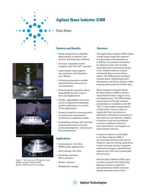
Figure 1. Top: close-up of XP indenter head.<br />
Middle: the <strong>Nano</strong> <strong>Indenter</strong> <strong>G300</strong>.<br />
Bottom: <strong>G300</strong> vacuum chuck stages.<br />
Features and Benefits<br />
• Newly integrated tool simplifies<br />
determination of indenter area<br />
function and load-frame stiffness<br />
• Accurate, repeatable results<br />
compliant with ISO 14577 standard<br />
• Large sample stage supports<br />
test specimens with diameters<br />
up to 300mm<br />
• Full testing automation enables<br />
nanoindentation instrument to<br />
run unattended<br />
• Electromagnetic actuation allows<br />
unparalleled dynamic range in<br />
force and displacement<br />
• Flexible, upgradeable instrument<br />
can be configured for repeatable<br />
specific applications or a variety<br />
of new applications<br />
• Dynamic properties characterization<br />
via continuous measurement<br />
of stiffness by indentation depth<br />
• Outstanding software with real-time<br />
experimental control, easy test<br />
protocol development, and precision<br />
drift compensation<br />
Applications<br />
• Semiconductor, thin films,<br />
MEMs (wafer applications)<br />
• Hard coatings, DLC films<br />
• Composite materials,<br />
fibers, polymers<br />
• Metals, ceramics<br />
• Biomaterials, biology<br />
Overview<br />
The <strong>Agilent</strong> <strong>Nano</strong> <strong>Indenter</strong> <strong>G300</strong> utilizes<br />
a large sample stage that supports<br />
test specimens with diameters up<br />
to 300mm. An excellent investment<br />
for industrial users, this versatile<br />
nanoindentation instrument provides<br />
a fast, reliable method to acquire<br />
mechanical data on uncut silicon<br />
wafers. The <strong>G300</strong> permits testing of<br />
multiple layers, facilitating product<br />
development and failure analysis, while<br />
keeping wafers intact for further tests.<br />
Electromagnetic actuation allows<br />
the <strong>Nano</strong> <strong>Indenter</strong> <strong>G300</strong> to achieve<br />
unparalleled dynamic range in force<br />
and displacement. The <strong>G300</strong> enables<br />
measurement of Young’s modulus<br />
and hardness in compliance with ISO<br />
14577. It also enables measurement<br />
of deformation over six orders of<br />
magnitude (from nanometers to<br />
millimeters). Mechanical properties at<br />
this scale such as hardness, modulus<br />
of elasticity, and fracture behavior<br />
can have a significant effect on<br />
yield, performance, and longevity of<br />
semiconductor devices.<br />
A variety of options can be added<br />
to the <strong>Nano</strong> <strong>Indenter</strong> <strong>G300</strong> to<br />
accommodate testing needs such as<br />
frequency-specific testing, quantitative<br />
scratch and wear testing, integrated<br />
probe-based imaging, expanded load<br />
capacity up to 10N, and customizable<br />
test protocols.<br />
With the <strong>Nano</strong> <strong>Indenter</strong> <strong>G300</strong>, users<br />
are able to quantify the relationship<br />
between structure, properties,<br />
and performance of their materials<br />
quickly and easily with minimal
sample preparation. The user-friendly<br />
design of the <strong>G300</strong> simplifies training<br />
requirements — standard tests can<br />
be run on the same day the instrument<br />
is installed. Every <strong>G300</strong> is backed by<br />
highly responsive <strong>Agilent</strong> <strong>Technologies</strong><br />
customer service personnel.<br />
Knowledgeable and experienced<br />
regional applications engineers are<br />
available to guide users through more<br />
advanced testing, provide outstanding<br />
technical support, and offer unmatched<br />
applications expertise.<br />
Advanced Design<br />
All nanoindentation experiments rely<br />
on the accuracy of the fundamental<br />
load and the displacement data,<br />
requiring the highest precision control<br />
of load applied to the sample. The<br />
<strong>Nano</strong> <strong>Indenter</strong> <strong>G300</strong> is powered by<br />
electromagnetic actuation-based<br />
force transducers to ensure precise<br />
measurements; users can program<br />
experiments with each force transducer<br />
and switch between them at any time.<br />
The instrument’s unique design avoids<br />
lateral displacement artifacts, while<br />
software compensates fully for any drift<br />
in force.<br />
The <strong>Nano</strong> <strong>Indenter</strong> <strong>G300</strong> is software<br />
controlled and simple to use. Operators<br />
need only decide where to place the<br />
indentations and what experiments to<br />
perform at those positions. Full testing<br />
automation enables the instrument to<br />
run unattended and report results in<br />
both Microsoft ® Word and Excel. The<br />
<strong>G300</strong> can help streamline materials<br />
selection processes and large-scale<br />
industrial testing.<br />
New Enhanced Dynamic<br />
Contact Module II Option<br />
The <strong>Nano</strong> <strong>Indenter</strong> <strong>G300</strong> standard<br />
configuration utilizes the <strong>Agilent</strong> XP<br />
indentation head, which delivers<br />
500µm maximum indentation<br />
depth. To extend the range of<br />
load-displacement experimentation<br />
to the surface contact level, the <strong>G300</strong><br />
can be equipped with the new <strong>Agilent</strong><br />
Dynamic Contact Module II (DCM II)<br />
option. This option offers all of the<br />
impressive performance afforded by<br />
<strong>Agilent</strong>’s original DCM option as well<br />
as several new advantages, including<br />
3x higher loading capability (30mN<br />
max load), easy tip exchange for quick<br />
removal and installation of applicationspecific<br />
tips, and a full 70µm range of<br />
indenter travel.<br />
With the DCM II option, researchers<br />
can study not only the first few<br />
nanometers of an indentation into the<br />
surface of a material, but even the<br />
pre-contact mechanics. At this scale,<br />
the noise level of the indentation<br />
system also must be optimized to<br />
enhance its actual displacement<br />
measurement capability. Using standard<br />
methods, the displacement resolution<br />
of the DCM II is determined to be<br />
0.0002nm (0.2 picometers). Even more<br />
importantly, real-world testing shows<br />
that the noise levels are typically less<br />
than an angstrom, ensuring the best<br />
resolution of any indenter on the market<br />
today. The DCM II has the lowest noise<br />
floor of any instrument of its type.<br />
Continuous Stiffness<br />
Measurement (CSM) Option<br />
In conventional quasi-static indentation<br />
testing, the stiffness of contact is<br />
determined by analyzing the force vs.<br />
displacement curve during unloading.<br />
This depth-sensing method provides<br />
a single measurement for the given<br />
indentation depth. The <strong>Agilent</strong><br />
Continuous Stiffness Measurement<br />
(CSM) technique, which is compatible<br />
with both the XP and the DCM II<br />
indentation heads, satisfies application<br />
requirements that must take into<br />
account dynamic effects, such as strain<br />
rate and frequency.<br />
With the CSM option, the <strong>Nano</strong><br />
<strong>Indenter</strong> <strong>G300</strong> applies a load to the<br />
indenter tip to force the tip into<br />
the surface while simultaneously<br />
superimposing an oscillating force with<br />
a force amplitude generally several<br />
orders of magnitude smaller than the<br />
nominal load. The CSM option offers<br />
a means of separating the in-phase<br />
and out-of-phase components of<br />
the load-displacement history. This<br />
separation provides an accurate<br />
measurement of the location of initial<br />
surface contact and continuous<br />
measurement of contact stiffness as<br />
a function of depth or frequency, thus<br />
eliminating the need for unloading<br />
cycles. Since the contact stiffness is<br />
determined directly, no assumptions<br />
(such as mechanical equilibrium) are<br />
required to correct for elasticity.<br />
The <strong>G300</strong> includes a motorized sample<br />
manipulation table with mouse<br />
control, a vibration isolation table and<br />
environmental enclosure, an optical<br />
imaging system, a video camera<br />
with frame-grabbing software, and a<br />
pre-mounted diamond indentation tip.<br />
The <strong>G300</strong> also includes a softwarecontrolled,<br />
automated handset as<br />
well as a fully automated data<br />
acquisition and control system with<br />
PC, monitor, keyboard, color inkjet<br />
printer, and <strong>Agilent</strong> <strong>Nano</strong>Suite 6.1<br />
Professional software.<br />
Figure 2. Low-k film normalized by percent of film thickness. Non-destructive testing was done at<br />
predetermined sites using with a method that allows collection of substrate-independent properties<br />
of your film.<br />
2
This makes CSM a powerful tool not<br />
only for stiff materials such as metals,<br />
alloys, and ceramics but also for<br />
time-dependent materials like polymers,<br />
structural composites, and biomedical<br />
materials.<br />
The state-of-the-art CSM option<br />
provides the only means available<br />
to both fully characterize dynamic<br />
properties in the nanometer range and<br />
accurately characterize viscoelastic<br />
materials providing values such as<br />
storage modulus. Indentation tests<br />
using CSM can be controlled with a<br />
constant strain rate, a critical test<br />
parameter for material systems such as<br />
pure metals or low-melting-point alloys,<br />
and polymer films and film/substrate<br />
systems. This level of control is not<br />
possible with the conventional method.<br />
Lateral Force Measurement<br />
(LFM) Option<br />
There are several additional<br />
performance-extending <strong>Nano</strong><br />
<strong>Indenter</strong> <strong>G300</strong> options available for<br />
use with the standard XP indentation<br />
head. The <strong>Agilent</strong> Lateral Force<br />
Measurement (LFM) option provides<br />
three-dimensional quantitative analysis<br />
for scratch testing, wear testing, and<br />
MEMS probing. This option enables<br />
force detection in the X and Y directions<br />
to examine shear forces. Tribological<br />
studies benefit greatly from the LFM<br />
option for determination of the critical<br />
load and coefficient of friction over the<br />
scratch length.<br />
High Load Option<br />
The capabilities of the <strong>Nano</strong> <strong>Indenter</strong><br />
<strong>G300</strong> can also be enhanced via the<br />
<strong>Agilent</strong> High Load option. Designed for<br />
use with the standard XP indentation<br />
head, this option expands the load<br />
capabilities of the <strong>Nano</strong> <strong>Indenter</strong><br />
<strong>G300</strong> up to 10N of force, allowing the<br />
complete mechanical characterization<br />
of ceramics, bulk metals, and<br />
composites. The High Load option has<br />
been engineered to avoid sacrificing<br />
the instrument’s load and displacement<br />
resolutions at low forces while<br />
seamlessly engaging at the point in<br />
the test protocol when extra force is<br />
required.<br />
New Enhanced <strong>Nano</strong>Suite 6.1<br />
Professional Software<br />
Every <strong>Nano</strong> <strong>Indenter</strong> <strong>G300</strong> comes with<br />
<strong>Agilent</strong> <strong>Nano</strong>Suite 6.1 Professional<br />
software, a premium-performance<br />
package that gives researchers in<br />
scientific and industrial settings<br />
an unprecedented combination of<br />
speed, flexibility, and ease of use.<br />
<strong>Nano</strong>Suite 6.1 offers a variety of brand<br />
new, prewritten test methods, including<br />
an exclusive nanoindentation technique<br />
for making substrate-independent<br />
measurements of thin film materials,<br />
several novel techniques for testing<br />
polymers, and improved scratch test<br />
methods. <strong>Agilent</strong>’s field-proven method<br />
for testing in compliance with ISO<br />
14577, the international standard for<br />
indentation testing, is provided<br />
as well.<br />
<strong>Nano</strong>Suite 6.1 even includes a fully<br />
integrated tool that greatly simplifies<br />
the determination of indenter area<br />
function and load-frame stiffness. Once<br />
a rather involved and time-consuming<br />
endeavor, this process now requires<br />
only a couple of mouse-clicks within<br />
the <strong>Nano</strong>Suite 6.1 program. Prewritten<br />
methods for testing gels (DCM II<br />
indentation head and CSM option<br />
required) and for measuring strain-rate<br />
sensitivity (XP indentation head and<br />
CSM option required) have also been<br />
added to <strong>Nano</strong>Suite 6.1.<br />
Additional new capabilities allow a<br />
standard batch of tests comprising<br />
25 or more samples to be set up in 5<br />
minutes or less, 2D graphs to be plotted<br />
on-screen and exported directly to<br />
<strong>Nano</strong>indentation instruments from <strong>Agilent</strong> <strong>Technologies</strong> conform to the<br />
ISO 14577 standard, delivering confidence in test accuracy and repeatability.<br />
These state-of-the-art solutions ensure reliable, high-precision measurement<br />
of nanomechanical properties for research and industry.<br />
Figure 3. The <strong>G300</strong> tests for the adhesion of<br />
film. This image shows the delamination of a<br />
polymer film on glass.<br />
Microsoft Excel while preserving all<br />
labels and scales, and sample files to<br />
be organized by project and subproject.<br />
<strong>Nano</strong>Suite 6.1 also provides Microsoft<br />
Windows 7 (32-bit) compliance for<br />
current systems and a convenient PDF<br />
printer to replace hardware printers.<br />
As in the package’s previous iteration,<br />
an intuitive interface allows users to<br />
set up and run experiments quickly<br />
— changing test parameters as often<br />
as desired — with just a few clicks.<br />
<strong>Nano</strong>Suite 6.1 offers support of small<br />
force/displacement measurements,<br />
surface topology, stiffness mapping,<br />
scratch tests, and more. Versatile<br />
imaging capabilities, a survey scanning<br />
option, and streamlined test method<br />
development help researchers get from<br />
testing to results in record time.<br />
<strong>Nano</strong>Vision Software Option<br />
The <strong>Agilent</strong> <strong>Nano</strong>Vision option for the<br />
<strong>Nano</strong> <strong>Indenter</strong> <strong>G300</strong> is used to probe the<br />
surface of a sample, generating a 3D map<br />
of the surface. Backed by decades of<br />
nanomechanical testing experience, the<br />
<strong>Nano</strong>Vision nanomechanical microscopy<br />
option delivers quantitative imaging<br />
by coupling a linear electromagnetic<br />
actuation-based indentation head<br />
with a closed-loop nanopositioning<br />
stage. <strong>Nano</strong>Vision allows users to<br />
create quantitative high-resolution<br />
images using a <strong>Nano</strong> <strong>Indenter</strong> <strong>G300</strong>,<br />
target indentation test sites with<br />
nanometer-scale precision, and examine<br />
residual impressions in order to quantify<br />
material response phenomena such as<br />
pile-up, deformed volume, and fracture<br />
toughness. This option also lets users<br />
target and characterize individual phases<br />
of complex materials.<br />
3
<strong>Agilent</strong> <strong>Nano</strong> <strong>Indenter</strong> <strong>G300</strong> Specifications<br />
Standard XP Indentation Head<br />
Displacement resolution<br />
500µm<br />
Load application<br />
Coil / magnet assembly<br />
Displacement measurement<br />
Capacitance gauge<br />
Loading capability<br />
Maximum load (standard)<br />
500mN<br />
Maximum load with DCM II option 30mN<br />
Maximum load with High Load option 10N<br />
Load resolution<br />
50nN<br />
Contact force<br />
120Hz<br />
<strong>Nano</strong> Mechanical Systems from<br />
<strong>Agilent</strong> <strong>Technologies</strong><br />
<strong>Agilent</strong> <strong>Technologies</strong>, the premier<br />
measurement company, offers highprecision,<br />
modular nano-measurement<br />
solutions for research, industry, and<br />
education. Exceptional worldwide support<br />
is provided by experienced application<br />
scientists and technical service personnel.<br />
<strong>Agilent</strong>’s leading-edge R&D laboratories<br />
ensure the continued, timely introduction<br />
and optimization of innovative, easy-to-use<br />
nanomechanical system technologies.<br />
www.agilent.com/find/nanoindenter<br />
Americas<br />
Canada (877) 894 4414<br />
Latin America 305 269 7500<br />
United States (800) 829 4444<br />
Asia Pacific<br />
Australia 1 800 629 485<br />
China 800 810 0189<br />
Hong Kong 800 938 693<br />
India 1 800 112 929<br />
Japan 0120 (421) 345<br />
Korea 080 769 0800<br />
Malaysia 1 800 888 848<br />
Singapore 1 800 375 8100<br />
Taiwan 0800 047 866<br />
Thailand 1 800 226 008<br />
Europe & Middle East<br />
Austria 43 (0) 1 360 277 1571<br />
Belgium 32 (0) 2 404 93 40<br />
Denmark 45 70 13 15 15<br />
Finland 358 (0) 10 855 2100<br />
France 0825 010 700*<br />
*0.125 €/minute<br />
Germany 49 (0) 7031 464 6333<br />
Ireland 1890 924 204<br />
Israel 972-3-9288-504/544<br />
Italy 39 02 92 60 8484<br />
Netherlands 31 (0) 20 547 2111<br />
Spain 34 (91) 631 3300<br />
Sweden 0200-88 22 55<br />
Switzerland 0800 80 53 53<br />
United Kingdom 44 (0) 118 9276201<br />
Other European Countries:<br />
www.agilent.com/find/contactus<br />
Product specifications and descriptions in this<br />
document subject to change without notice.<br />
© <strong>Agilent</strong> <strong>Technologies</strong>, Inc. 2012<br />
Printed in USA, March 28, 2012<br />
5990-4178EN RevD