Atomic layer deposition of GaN using GaCl3 and NH3
Atomic layer deposition of GaN using GaCl3 and NH3
Atomic layer deposition of GaN using GaCl3 and NH3

Create successful ePaper yourself
Turn your PDF publications into a flip-book with our unique Google optimized e-Paper software.
924 Kim, Kim, <strong>and</strong> Anderson: <strong>Atomic</strong> <strong>layer</strong> <strong>deposition</strong> <strong>of</strong> <strong>GaN</strong> <strong>using</strong> GaCl 3 <strong>and</strong> NH 3 924<br />
48 °C to allow easy delivery. The microstructure, Cl content,<br />
<strong>and</strong> chemical bonding states were examined for films<br />
grown within the ALD process window.<br />
II. EXPERIMENTAL PROCEDURES<br />
In this study, one ALD cycle consisted <strong>of</strong> four steps <strong>of</strong><br />
sequential gas supplies: 1 GaCl 3 /N 2 carrier, 2 N 2 purge,<br />
3 NH 3 /N 2 carrier, <strong>and</strong> 4 N 2 purge. The ALD growth<br />
mechanism <strong>of</strong> <strong>GaN</strong> <strong>using</strong> GaCl 3 <strong>and</strong> NH 3 is anticipated to be<br />
similar to that <strong>of</strong> TiN <strong>using</strong> TiCl 4 <strong>and</strong> NH 3 . 5 During the first<br />
step, input GaCl 3 adsorbs on the surface active sites to form<br />
GaCl x x3. Any remaining GaCl 3 or physisorbed byproducts<br />
are purged from the reactor in the second step.<br />
Next, NH 3 reacts with adsorbed GaCl x to form chemisorbed<br />
<strong>GaN</strong>H 3−x <strong>and</strong> xHCl as a physisorbed by-product. The remaining<br />
NH 3 <strong>and</strong> physisorbed HCl are finally purged upon<br />
exposure to the N 2 carrier in the last step.<br />
ALD <strong>of</strong> <strong>GaN</strong> on Si100 was performed in a custom horizontal<br />
quartz reactor equipped with a load-lock system.<br />
Pneumatically actuated valves, controlled with a LABVIEWbased<br />
algorithm, were sequenced to deliver each reactant <strong>and</strong><br />
purge gas to the reactor or bypass line. The Si100 surface<br />
was degreased trichloroethylene, acetone, <strong>and</strong> methanol,<br />
followed by a buffered oxide etch 2 min. GaCl 3 99.999%,<br />
Sigma Aldrich was contained in a bubbler maintained at<br />
70 °C <strong>and</strong> delivered to the reactor in N 2 99.999%, Praxair<br />
carrier gas. NH 3 99.9999%, Matheson Tri-Gas was used as<br />
the reactive nitrogen source <strong>and</strong> N 2 as the purge gas. <strong>GaN</strong><br />
films were deposited in the temperature range <strong>of</strong><br />
375–750 °C at a nominal growth pressure <strong>of</strong> 1 Torr. One<br />
ALD cycle consisted <strong>of</strong> sequential GaCl 3 supply 50 sccm<br />
N 2 sccm denotes cubic centimeters per minute at STP, N 2<br />
purge 30 s, 500 sccm, NH 3 supply 500 sccm, <strong>and</strong> N 2<br />
purge 30 s, 500 sccm.<br />
The film thickness was measured by cross-sectional scanning<br />
electron microscopy SEM <strong>and</strong> x-ray reflectometry<br />
XRR <strong>using</strong> a JEOL JSM-6335F SEM <strong>and</strong> a Philips MRD<br />
X’Pert system, respectively. Grazing incident angle x-ray<br />
diffraction GIXD <strong>using</strong> a Philips MRD X’Pert system operating<br />
with Cu K radiation 40 kV <strong>and</strong> 40 mA was used<br />
to characterize the film microstructure. GIXD was performed<br />
from 30° to 40° 2 at 1° tilt. <strong>Atomic</strong> force microscopy<br />
AFM Digital Instruments Dimension 3100 was used to<br />
examine the film surface morphology. To investigate chemical<br />
bonding states, x-ray photoelectron spectroscopy XPS<br />
measurements were performed with a PerkinElmer PH1<br />
ESCA system. Monochromatic Mg K ionizing radiation<br />
1254 eV was used with the x-ray source operating at<br />
300 W 15 kV <strong>and</strong> 20 mA. To remove surface contamination,<br />
as-grown films were sputtered with Ar + ions for 10 min<br />
prior to XPS measurement.<br />
III. RESULTS AND DISCUSSION<br />
A. Confirmation <strong>of</strong> self-saturation ALD growth<br />
To verify that growth occurred in ALD mode, a set <strong>of</strong><br />
experiments was performed to identify a growth window in<br />
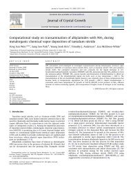
FIG. 1. Dependence <strong>of</strong> ALD <strong>GaN</strong> growth rate on GaCl 3 exposure time at<br />
T growth =a 550 °C <strong>and</strong> b 650 °C. These films are grown on Si100 with<br />
NH 3 exposure time <strong>of</strong> 10 s.<br />
temperature <strong>and</strong> GaCl 3 exposure time that produced selflimiting<br />
growth. To this end, a series <strong>of</strong> films was grown<br />
150 cycles in which the exposure time was varied in the<br />
range <strong>of</strong> 2–17 s at a fixed NH 3 exposure time <strong>of</strong> 10 s <strong>and</strong> N 2<br />
purge time <strong>of</strong> 30 s. Figures 1a <strong>and</strong> 1b show the growth<br />
rate film thickness per cycle as a function <strong>of</strong> GaCl 3 exposure<br />
time at growth temperature <strong>of</strong> 550 <strong>and</strong> 650 °C, respectively.<br />
The results in Fig. 1a suggest that the growth rate at<br />
550 °C remains constant at 2.00.4 Å/cycle in the range <strong>of</strong><br />
4–11 s <strong>of</strong> GaCl 3 exposure time. The measurements at the<br />
higher growth temperature, 650 °C, show a similar growth<br />
plateau at 2.10.5 Å/cycle, but as expected, a narrower exposure<br />
time window GaCl 3 exposure time in the range <strong>of</strong><br />
5–9 s. The constant thickness/cycle regime versus reactant<br />
exposure is a feature <strong>of</strong> ALD <strong>and</strong> indicates that GaCl 3 is<br />
incorporated by self-limiting adsorption.<br />
The <strong>deposition</strong> rate in the saturation growth regime was<br />
1.6–2.6 Å/cycle. As subsequently presented, the microstructure<br />
<strong>of</strong> ALD-<strong>GaN</strong> in this process window is a mixture <strong>of</strong><br />
0002 <strong>and</strong> 101¯1 oriented <strong>GaN</strong>. Thus, the thickness <strong>of</strong> 1<br />
ML <strong>of</strong> ALD-<strong>GaN</strong> is calculated as 5.58 Å. Therefore, the<br />
<strong>deposition</strong> rate in saturation growth regime is 29%–47% <strong>of</strong><br />
1ML/cycle. It is commonly reported that the saturation coverage<br />
<strong>of</strong> the metal-containing precursor for most metal nitride<br />
ALD reactions is less than a single mono<strong>layer</strong>. 10 An<br />
<strong>of</strong>ten cited reason is that steric hindrance <strong>of</strong> adsorbed metal<br />
precursors prevents mono<strong>layer</strong> coverage. 5<br />
The results in Fig. 1 show that the growth rate linearly<br />
increases for GaCl 3 exposure time greater than the window<br />
limit, with the rate <strong>of</strong> increase greater at the lower temperature.<br />
An increase in growth rate with exposure time is usually<br />
ascribed to continued chemisorption beyond the saturation<br />
J. Vac. Sci. Technol. A, Vol. 27, No. 4, Jul/Aug 2009