Atomic layer deposition of GaN using GaCl3 and NH3
Atomic layer deposition of GaN using GaCl3 and NH3
Atomic layer deposition of GaN using GaCl3 and NH3

Create successful ePaper yourself
Turn your PDF publications into a flip-book with our unique Google optimized e-Paper software.
<strong>Atomic</strong> <strong>layer</strong> <strong>deposition</strong> <strong>of</strong> <strong>GaN</strong> <strong>using</strong> GaCl 3 <strong>and</strong> NH 3<br />
Oh Hyun Kim, Dojun Kim, <strong>and</strong> Tim Anderson a<br />
Department <strong>of</strong> Chemical Engineering, University <strong>of</strong> Florida, Gainesville, Florida 32611-6005<br />
Received 20 October 2008; accepted 2 March 2009; published 30 June 2009<br />
<strong>GaN</strong> films were grown on Si100 substrate by atomic <strong>layer</strong> <strong>deposition</strong> ALD <strong>using</strong> GaCl 3 <strong>and</strong><br />
NH 3 . Growth conditions were identified for which the growth rate exhibited a plateau at<br />
2.0 Å/cycle, consistent with self-limiting adsorption. A relatively wide temperature window<br />
500–750 °C for ALD growth mode was also established for one flow sequence schedule. In this<br />
limit, both the 0002 <strong>and</strong> 101¯1 orientations <strong>of</strong> <strong>GaN</strong> were evident, which was attributed to the<br />
competition between vertical <strong>and</strong> lateral growths. Cl incorporation was detected by x-ray<br />
photoelectron spectroscopy for samples prepared with long GaCl 3 exposure time. It is postulated<br />
that gas phase formation <strong>of</strong> Cl<strong>GaN</strong>H n with n=1–3 Kovács, Inorg. Chem. 41, 3067 2002<br />
results in higher Cl content. © 2009 American Vacuum Society. DOI: 10.1116/1.3106619<br />
I. INTRODUCTION<br />
Group III nitrides have found wide application in both<br />
electronic <strong>and</strong> optoelectronic devices. In particular, solid solutions<br />
<strong>of</strong> the direct b<strong>and</strong>-gap nitrides can access the entire<br />
visible range <strong>of</strong> the spectrum as well as the near UV. Furthermore,<br />
the relatively high thermal stability <strong>of</strong> <strong>GaN</strong> <strong>and</strong><br />
AlN has made these nitrides useful in power electronics.<br />
Sapphire is commonly used as substrate for growth <strong>of</strong> <strong>GaN</strong>,<br />
but the low cost, high crystalline quality, <strong>and</strong> large area <strong>of</strong> Si<br />
make it an attractive substrate choice. In practice, the nitrides<br />
are typically deposited by metal organic chemical vapor<br />
<strong>deposition</strong> MOCVD, <strong>and</strong> for <strong>GaN</strong> <strong>layer</strong>s, a <strong>deposition</strong> temperature<br />
in the range <strong>of</strong> 900–1100 °C is needed to produce<br />
device quality material. Although the rate <strong>of</strong> NH 3 cracking is<br />
greater at higher temperature, the nitrogen partial pressure in<br />
equilibrium with the compound is also higher, which leads to<br />
a high concentration <strong>of</strong> nitrogen vacancies in the <strong>GaN</strong> film.<br />
This higher vacancy concentration is reported to be the reason<br />
for the high background-carrier concentration in<br />
MOCVD grown <strong>GaN</strong>. 1 Thus, a lower growth temperature is<br />
preferred to reduce background-carrier concentration. 2 In<br />
contrast, the thermal stability <strong>of</strong> InN is considerably less than<br />
that <strong>of</strong> <strong>GaN</strong> <strong>and</strong> AlN, <strong>and</strong> thus growth is typically limited to<br />
a temperature below 800 °C. Also, a lower growth temperature<br />
is preferred for growth <strong>of</strong> In x Ga 1−x N. Lowering the<br />
growth temperature in MOCVD, however, does present difficulties.<br />
At lower growth temperature the surface mobility <strong>of</strong><br />
adsorbed species is reduced, which produces films with<br />
poorer structural quality <strong>and</strong> hence optical properties. As example,<br />
it has been reported that In x Ga 1−x N grown at 500 °C<br />
shows 1000 times weaker photoluminescence than material<br />
grown at 800 °C. 3 Another issue at lower growth temperature<br />
is a decreased extent <strong>of</strong> NH 3 thermal decomposition.<br />
Thus both poor mobility <strong>of</strong> surface species <strong>and</strong> the low<br />
availability <strong>of</strong> reactive nitrogen make growth at low temperature<br />
challenging.<br />
a Electronic mail: tim@ufl.edu<br />
<strong>Atomic</strong> <strong>layer</strong> <strong>deposition</strong> ALD is a potential solution to<br />
these growth issues. Since sequential delivery <strong>of</strong> the reactants<br />
in a self-limiting adsorption mode affords increased<br />
residence time, both the extent <strong>of</strong> species surface transport<br />
<strong>and</strong> chemical reaction are increased. This allows for improved<br />
structural quality as well as increased levels <strong>of</strong> reactive<br />
nitrogen. Thus ALD films <strong>of</strong> acceptable quality can <strong>of</strong>ten<br />
be grown at lower temperature than by CVD. As example,<br />
ALD growth <strong>of</strong> device quality GaAs, GaP, <strong>and</strong> InGaP has<br />
been demonstrated at a temperature <strong>of</strong> as low as 200 °C. 4<br />
Of course, ALD gives control <strong>of</strong> the film thickness at the<br />
atomic <strong>layer</strong> <strong>and</strong> shows improved reproducibility <strong>of</strong> alloy<br />
composition. 5 Potential drawbacks <strong>of</strong> ALD are the lower<br />
growth rate <strong>and</strong> the fact that impurities can more effectively<br />
compete for adsorption sites, <strong>and</strong> thus increase impurity concentration<br />
levels.<br />
Unfortunately, very little work has been reported on ALD<br />
<strong>of</strong> <strong>GaN</strong>. Early studies <strong>of</strong> ALD growth <strong>of</strong> <strong>GaN</strong> used a Ga<br />
metal organic source trimethylgallium TMG <strong>and</strong> trithylgallium<br />
TEG <strong>and</strong> NH 3 . 2,6,7 Films were grown on sapphire or<br />
AlN, <strong>and</strong> self-limiting adsorption region was shown with Ga<br />
source exposure time. The growth temperature window,<br />
however, was not investigated in these studies. The relatively<br />
unstable MO sources show a narrow process temperature<br />
window for most materials. To resolve this issue, Ga chloride<br />
sources GaCl <strong>and</strong> GaCl 3 have been used with NH 3 in ALD<br />
growth mode on GaAs or <strong>GaN</strong>/GaAs. 8,9 In these studies, the<br />
self-limiting adsorption region was evident with GaCl exposure<br />
time, <strong>and</strong> a temperature window was found when <strong>using</strong><br />
GaCl. Films showed either hexagonal or cubic <strong>GaN</strong>002<br />
preferred orientation. The self-limiting adsorption windows,<br />
however, were not established for use <strong>of</strong> GaCl 3 . Also, Cl<br />
incorporation in the film, which is critical to the device performance,<br />
was not considered. This study conclusively demonstrates<br />
ALD <strong>of</strong> <strong>GaN</strong> on Si100 for the first time <strong>using</strong><br />
GaCl 3 <strong>and</strong> NH 3 sources. It is suggested that GaCl 3 is a superior<br />
source because <strong>of</strong> its thermal stability in an H 2 -free<br />
adsorption step, which increases the width <strong>of</strong> the temperature<br />
window. GaCl 3 is also sufficiently volatile 1 mmHg at<br />
923 J. Vac. Sci. Technol. A 27„4…, Jul/Aug 2009 0734-2101/2009/27„4…/923/6/$25.00 ©2009 American Vacuum Society 923
924 Kim, Kim, <strong>and</strong> Anderson: <strong>Atomic</strong> <strong>layer</strong> <strong>deposition</strong> <strong>of</strong> <strong>GaN</strong> <strong>using</strong> GaCl 3 <strong>and</strong> NH 3 924<br />
48 °C to allow easy delivery. The microstructure, Cl content,<br />
<strong>and</strong> chemical bonding states were examined for films<br />
grown within the ALD process window.<br />
II. EXPERIMENTAL PROCEDURES<br />
In this study, one ALD cycle consisted <strong>of</strong> four steps <strong>of</strong><br />
sequential gas supplies: 1 GaCl 3 /N 2 carrier, 2 N 2 purge,<br />
3 NH 3 /N 2 carrier, <strong>and</strong> 4 N 2 purge. The ALD growth<br />
mechanism <strong>of</strong> <strong>GaN</strong> <strong>using</strong> GaCl 3 <strong>and</strong> NH 3 is anticipated to be<br />
similar to that <strong>of</strong> TiN <strong>using</strong> TiCl 4 <strong>and</strong> NH 3 . 5 During the first<br />
step, input GaCl 3 adsorbs on the surface active sites to form<br />
GaCl x x3. Any remaining GaCl 3 or physisorbed byproducts<br />
are purged from the reactor in the second step.<br />
Next, NH 3 reacts with adsorbed GaCl x to form chemisorbed<br />
<strong>GaN</strong>H 3−x <strong>and</strong> xHCl as a physisorbed by-product. The remaining<br />
NH 3 <strong>and</strong> physisorbed HCl are finally purged upon<br />
exposure to the N 2 carrier in the last step.<br />
ALD <strong>of</strong> <strong>GaN</strong> on Si100 was performed in a custom horizontal<br />
quartz reactor equipped with a load-lock system.<br />
Pneumatically actuated valves, controlled with a LABVIEWbased<br />
algorithm, were sequenced to deliver each reactant <strong>and</strong><br />
purge gas to the reactor or bypass line. The Si100 surface<br />
was degreased trichloroethylene, acetone, <strong>and</strong> methanol,<br />
followed by a buffered oxide etch 2 min. GaCl 3 99.999%,<br />
Sigma Aldrich was contained in a bubbler maintained at<br />
70 °C <strong>and</strong> delivered to the reactor in N 2 99.999%, Praxair<br />
carrier gas. NH 3 99.9999%, Matheson Tri-Gas was used as<br />
the reactive nitrogen source <strong>and</strong> N 2 as the purge gas. <strong>GaN</strong><br />
films were deposited in the temperature range <strong>of</strong><br />
375–750 °C at a nominal growth pressure <strong>of</strong> 1 Torr. One<br />
ALD cycle consisted <strong>of</strong> sequential GaCl 3 supply 50 sccm<br />
N 2 sccm denotes cubic centimeters per minute at STP, N 2<br />
purge 30 s, 500 sccm, NH 3 supply 500 sccm, <strong>and</strong> N 2<br />
purge 30 s, 500 sccm.<br />
The film thickness was measured by cross-sectional scanning<br />
electron microscopy SEM <strong>and</strong> x-ray reflectometry<br />
XRR <strong>using</strong> a JEOL JSM-6335F SEM <strong>and</strong> a Philips MRD<br />
X’Pert system, respectively. Grazing incident angle x-ray<br />
diffraction GIXD <strong>using</strong> a Philips MRD X’Pert system operating<br />
with Cu K radiation 40 kV <strong>and</strong> 40 mA was used<br />
to characterize the film microstructure. GIXD was performed<br />
from 30° to 40° 2 at 1° tilt. <strong>Atomic</strong> force microscopy<br />
AFM Digital Instruments Dimension 3100 was used to<br />
examine the film surface morphology. To investigate chemical<br />
bonding states, x-ray photoelectron spectroscopy XPS<br />
measurements were performed with a PerkinElmer PH1<br />
ESCA system. Monochromatic Mg K ionizing radiation<br />
1254 eV was used with the x-ray source operating at<br />
300 W 15 kV <strong>and</strong> 20 mA. To remove surface contamination,<br />
as-grown films were sputtered with Ar + ions for 10 min<br />
prior to XPS measurement.<br />
III. RESULTS AND DISCUSSION<br />
A. Confirmation <strong>of</strong> self-saturation ALD growth<br />
To verify that growth occurred in ALD mode, a set <strong>of</strong><br />
experiments was performed to identify a growth window in<br />
FIG. 1. Dependence <strong>of</strong> ALD <strong>GaN</strong> growth rate on GaCl 3 exposure time at<br />
T growth =a 550 °C <strong>and</strong> b 650 °C. These films are grown on Si100 with<br />
NH 3 exposure time <strong>of</strong> 10 s.<br />
temperature <strong>and</strong> GaCl 3 exposure time that produced selflimiting<br />
growth. To this end, a series <strong>of</strong> films was grown<br />
150 cycles in which the exposure time was varied in the<br />
range <strong>of</strong> 2–17 s at a fixed NH 3 exposure time <strong>of</strong> 10 s <strong>and</strong> N 2<br />
purge time <strong>of</strong> 30 s. Figures 1a <strong>and</strong> 1b show the growth<br />
rate film thickness per cycle as a function <strong>of</strong> GaCl 3 exposure<br />
time at growth temperature <strong>of</strong> 550 <strong>and</strong> 650 °C, respectively.<br />
The results in Fig. 1a suggest that the growth rate at<br />
550 °C remains constant at 2.00.4 Å/cycle in the range <strong>of</strong><br />
4–11 s <strong>of</strong> GaCl 3 exposure time. The measurements at the<br />
higher growth temperature, 650 °C, show a similar growth<br />
plateau at 2.10.5 Å/cycle, but as expected, a narrower exposure<br />
time window GaCl 3 exposure time in the range <strong>of</strong><br />
5–9 s. The constant thickness/cycle regime versus reactant<br />
exposure is a feature <strong>of</strong> ALD <strong>and</strong> indicates that GaCl 3 is<br />
incorporated by self-limiting adsorption.<br />
The <strong>deposition</strong> rate in the saturation growth regime was<br />
1.6–2.6 Å/cycle. As subsequently presented, the microstructure<br />
<strong>of</strong> ALD-<strong>GaN</strong> in this process window is a mixture <strong>of</strong><br />
0002 <strong>and</strong> 101¯1 oriented <strong>GaN</strong>. Thus, the thickness <strong>of</strong> 1<br />
ML <strong>of</strong> ALD-<strong>GaN</strong> is calculated as 5.58 Å. Therefore, the<br />
<strong>deposition</strong> rate in saturation growth regime is 29%–47% <strong>of</strong><br />
1ML/cycle. It is commonly reported that the saturation coverage<br />
<strong>of</strong> the metal-containing precursor for most metal nitride<br />
ALD reactions is less than a single mono<strong>layer</strong>. 10 An<br />
<strong>of</strong>ten cited reason is that steric hindrance <strong>of</strong> adsorbed metal<br />
precursors prevents mono<strong>layer</strong> coverage. 5<br />
The results in Fig. 1 show that the growth rate linearly<br />
increases for GaCl 3 exposure time greater than the window<br />
limit, with the rate <strong>of</strong> increase greater at the lower temperature.<br />
An increase in growth rate with exposure time is usually<br />
ascribed to continued chemisorption beyond the saturation<br />
J. Vac. Sci. Technol. A, Vol. 27, No. 4, Jul/Aug 2009
925 Kim, Kim, <strong>and</strong> Anderson: <strong>Atomic</strong> <strong>layer</strong> <strong>deposition</strong> <strong>of</strong> <strong>GaN</strong> <strong>using</strong> GaCl 3 <strong>and</strong> NH 3 925<br />
FIG. 2. Dependence <strong>of</strong> the growth rate on temperature. Exposure times were<br />
set as GaCl 3 =7 s, NH 3 =10 s, <strong>and</strong> N 2 purge=30 s.<br />
limit at longer time. The steeper increase in growth rate at<br />
lower temperature suggests that a second reaction occurs in<br />
competition, which may be desorption <strong>of</strong> a surface Ga species<br />
to more volatile GaCl by the reaction with residual HCl.<br />
The results <strong>of</strong> these experiments also show the commonly<br />
observed decrease in growth rate at metal exposure times<br />
less than that required for operation in the plateau region <strong>and</strong><br />
attributed to insufficient exposure time to reach saturation. It<br />
is noted that the rate <strong>of</strong> change in the growth rate was similar<br />
for both growth temperatures.<br />
FIG. 4.Color online Surface morphology <strong>of</strong> the <strong>GaN</strong> films deposited with<br />
9 s <strong>of</strong> GaCl 3 exposure time at 650 °C for a 5, b 10, c 15, <strong>and</strong> d<br />
150 cycles.<br />
B. Process temperature window<br />
FIG. 3. Dependence <strong>of</strong> film thickness XRR on the cycle number. Growth<br />
conditions were set as GaCl 3 exposure time=9 s, NH 3 exposure time<br />
=10 s, <strong>and</strong> N 2 purge time=30 s at T growth =650 °C.<br />
To further substantiate that growth occurs in ALD mode<br />
<strong>using</strong> this chemistry, a second set <strong>of</strong> experiments was performed<br />
to establish the extent <strong>of</strong> the temperature range yielding<br />
saturation-limited growth. In these experiments, <strong>deposition</strong>s<br />
were made at the self-saturation growth condition:<br />
GaCl 3 7 s, 50 sccm, N 2 purge 30 s, 500 sccm, <strong>and</strong> NH 3<br />
10 s, 500 sccm while varying the growth temperature in<br />
the range <strong>of</strong> 375–750 °C for runs <strong>of</strong> 150 cycles. As shown<br />
in Fig. 2, the growth rate increased with increasing growth<br />
temperature below 500 °C, but then remained constant<br />
2.10.2 Å/cycle above this temperature, which is consistent<br />
with operating in the ALD process temperature window.<br />
Since precursor adsorption onto a surface active site <strong>and</strong> reaction<br />
between adsorbed precursor <strong>and</strong> surface species are<br />
thermally activated processes, the growth temperature is expected<br />
to be an important factor. 5 At temperature below the<br />
window limit, there is insufficient thermal energy available<br />
to promote chemisorption at full coverage in the available<br />
exposure time. Within the ALD growth temperature window,<br />
there is sufficient thermal energy to reach the saturation condition<br />
but insufficient for additional reactions to occur e.g.,<br />
precursor decomposition <strong>and</strong> desorption that preclude saturation.<br />
An important feature <strong>of</strong> <strong>using</strong> a metal halide precursor<br />
is its high thermal stability, <strong>and</strong> thus the growth rate remains<br />
constant even at a relatively high growth temperature. It is<br />
noted that GaCl 3 does not react with N 2 in the temperature<br />
range <strong>of</strong> this study <strong>and</strong> also will not disproportionate since<br />
there is no reducing species available e.g., H 2 . Thus this Ga<br />
source seems well suited for ALD growth <strong>of</strong> <strong>GaN</strong>.<br />
C. Growth characteristic <strong>of</strong> <strong>GaN</strong> ALD<br />
Since the first <strong>layer</strong> to deposit requires adsorption on a Si<br />
or SiO x /Si surface, its growth characteristics are expected to<br />
be different from those <strong>layer</strong>s subsequently grown on the<br />
<strong>GaN</strong> surface. Furthermore, <strong>GaN</strong> is not well lattice matched<br />
to Si so that residual strain may persist for additional <strong>layer</strong>s<br />
to further modify the growth characteristics <strong>of</strong> <strong>layer</strong>s in the<br />
near Si/<strong>GaN</strong> interfacial region. Kinetic modeling <strong>and</strong> experimental<br />
results during the initial stages <strong>and</strong> the following stabilized<br />
stage have been reported. 11–13 To better underst<strong>and</strong><br />
the early stages <strong>of</strong> growth, a series <strong>of</strong> films was grown at<br />
identical conditions except with variable cycle number. The<br />
JVST A - Vacuum, Surfaces, <strong>and</strong> Films
926 Kim, Kim, <strong>and</strong> Anderson: <strong>Atomic</strong> <strong>layer</strong> <strong>deposition</strong> <strong>of</strong> <strong>GaN</strong> <strong>using</strong> GaCl 3 <strong>and</strong> NH 3 926<br />
FIG. 5. Color online GIXD patterns for a ALD-<strong>GaN</strong> <strong>and</strong> b CVD-<strong>GaN</strong><br />
films grown on Si100 at 650 °C.<br />
dependency <strong>of</strong> film thickness on the number <strong>of</strong> cycles was<br />
then examined by XRR. The ALD growth conditions were<br />
7 s <strong>of</strong> GaCl 3 exposure time at 650 °C with the other steps at<br />
the base conditions, while the cycle number was varied in the<br />
range 5–200.<br />
The results are shown in Fig. 3 <strong>and</strong> indicate that the<br />
growth rate <strong>of</strong> ALD-<strong>GaN</strong> gradually increased toward a constant<br />
value <strong>of</strong> 2.1 Å/cycle below 15 cycles, <strong>and</strong> this transition<br />
period is termed the transient stage. The growth rate<br />
becomes constant 2.10.2 Å/cycle above 15 cycles, exhibiting<br />
a linear dependency <strong>of</strong> film thickness on the cycle<br />
number. This is expected to occur because the adsorption<br />
characteristics <strong>of</strong> GaCl 3 on bare Si or SiO x /Si are different<br />
than those on N terminated <strong>GaN</strong>. During the first few cycles,<br />
self-limiting adsorption likely does not occur. However, once<br />
the surface is fully covered <strong>and</strong> presumably a few <strong>layer</strong>s<br />
thick, relaxed <strong>GaN</strong> becomes the growth surface, which allows<br />
self-limiting adsorption.<br />
During the transient stage, it is possible that the adsorption<br />
<strong>of</strong> reactants <strong>and</strong> preferential growth on as-deposited film<br />
compete, leading to three dimensional 3D growth. For example,<br />
studies on ALD <strong>of</strong> high- materials have reported 3D<br />
growth during the transient stage. 14 To probe this possibility<br />
for ALD-<strong>GaN</strong>, AFM images <strong>of</strong> the surface <strong>of</strong> films deposited<br />
in the transient stage were taken. Figure 4 depicts the surface<br />
morphology <strong>of</strong> ALD-<strong>GaN</strong> films grown for 5, 10, <strong>and</strong><br />
FIG. 6.Color online Surface morphology <strong>of</strong> the 60-nm-thick <strong>GaN</strong> films<br />
deposited at 650 °C under a ALD growth condition <strong>and</strong> b CVD growth<br />
condition.<br />
15 cycles. Figures 4a <strong>and</strong> 4b show that the surface roughness,<br />
R q root-mean-square roughness is relatively high for<br />
films grown with 5 <strong>and</strong> 10 cycles R q =0.84 nm for 5 cycles,<br />
R q =0.72 nm for 10 cycles, consistent with the 3D growth.<br />
The surface <strong>of</strong> the sample grown for 15 cycles Fig. 4c,<br />
however, is substantially smoother R q =0.55 nm. Note that<br />
the linear region begins at 15 cycles <strong>and</strong> is considered the<br />
point at which complete coverage <strong>of</strong> <strong>GaN</strong> on Si substrate is<br />
obtained. This conclusion is supported by noting that the<br />
surface roughness <strong>of</strong> the sample grown for 150 cycles Fig.<br />
4d is close to that <strong>of</strong> 15 cycles R q =0.58 nm.<br />
D. Film microstructure<br />
Given the differences in reaction time <strong>and</strong> delivery sequence,<br />
differences in microstructure between ALD <strong>and</strong><br />
CVD films might be expected. To explore this possibility,<br />
GIXD patterns <strong>of</strong> <strong>GaN</strong> film deposited in ALD mode were<br />
compared to those deposited outside the ALD process window<br />
at higher <strong>deposition</strong> rate <strong>and</strong> those deposited in CVD<br />
mode. GIXD patterns for all ALD <strong>GaN</strong> films are presented in<br />
Fig. 5a that reveals the change in the crystalline orientation<br />
for two different GaCl 3 exposure times. The lower GIXD<br />
pattern in Fig. 5a shows the result for the film grown in<br />
J. Vac. Sci. Technol. A, Vol. 27, No. 4, Jul/Aug 2009
927 Kim, Kim, <strong>and</strong> Anderson: <strong>Atomic</strong> <strong>layer</strong> <strong>deposition</strong> <strong>of</strong> <strong>GaN</strong> <strong>using</strong> GaCl 3 <strong>and</strong> NH 3 927<br />
(a)<br />
Ga 2p<br />
(b)<br />
N1s<br />
Intensity (a.u.)<br />
<strong>GaCl3</strong>=25 s<br />
<strong>GaCl3</strong>=15 s<br />
<strong>GaCl3</strong>=9s<br />
<strong>GaCl3</strong>=7 s<br />
Intensity (a.u.)<br />
<strong>GaCl3</strong>=25 s<br />
<strong>GaCl3</strong>=15 s<br />
<strong>GaCl3</strong>=9 s<br />
<strong>GaCl3</strong>=7 s<br />
<strong>GaCl3</strong>=2 s<br />
<strong>GaCl3</strong>=2 s<br />
1113 1118 1123<br />
Binding Energy (eV)<br />
394 396 398 400 402<br />
Binding Energy (eV)<br />
(c)<br />
O1s<br />
(d)<br />
Cl 2p<br />
<strong>GaCl3</strong>=25 s<br />
Intensity (a.u.)<br />
<strong>GaCl3</strong>=15 s<br />
<strong>GaCl3</strong>=9 s<br />
<strong>GaCl3</strong>=7 s<br />
<strong>GaCl3</strong>=2 s<br />
Intensity (a.u.)<br />
CVD<br />
<strong>GaCl3</strong>=25 s<br />
<strong>GaCl3</strong>=15 s<br />
<strong>GaCl3</strong>=9 s<br />
<strong>GaCl3</strong>=7 s<br />
<strong>GaCl3</strong>=2 s<br />
525 527 529 531 533 535<br />
Binding Energy (eV)<br />
195 197 199 201 203 205<br />
Binding Energy (eV)<br />
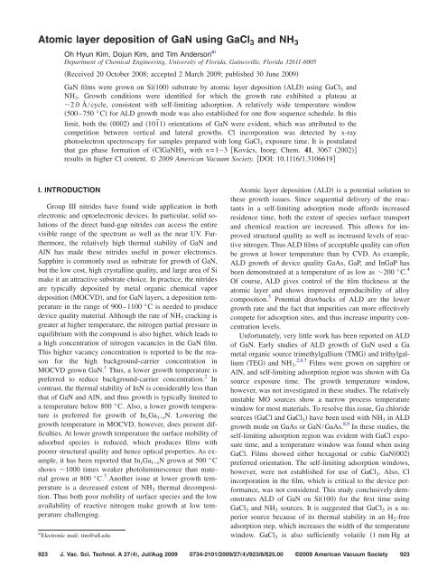
FIG. 7. Color online XPS spectra <strong>of</strong> a Ga 2p, b N1s, c O1s, <strong>and</strong> d Cl 2p measured for <strong>GaN</strong> film grown by ALD at various GaCl 3 exposure times.<br />
ALD mode with 7 s <strong>of</strong> GaCl 3 exposure time, while upper<br />
GIXD pattern shows the result for a film grown in CVD-like<br />
mode <strong>using</strong> 25 s <strong>of</strong> GaCl 3 exposure time. The GIXD patterns<br />
<strong>of</strong> both films indicate that their diffraction patterns are well<br />
matched with h-<strong>GaN</strong>0002 plane <strong>and</strong> h-<strong>GaN</strong>101¯1 plane,<br />
peak positions <strong>of</strong> 34.633° <strong>and</strong> 36.994° 2, respectively. 15 It<br />
is observed, however, that the h-<strong>GaN</strong>101¯1 <strong>and</strong><br />
h-<strong>GaN</strong>0002 peak intensities are similar for ALD film,<br />
while h-<strong>GaN</strong>0002 peak is dominant for the CVD-like film.<br />
The dominance <strong>of</strong> h-<strong>GaN</strong>0002 peak becomes more significant<br />
in the GIXD pattern <strong>of</strong> films grown in full CVD mode<br />
Fig. 5b. The significant presence <strong>of</strong> the h-<strong>GaN</strong>101¯1 reflection<br />
in self-saturation region is believed to be a result <strong>of</strong><br />
the lower growth rate. As shown in Fig. 1, the growth rate <strong>of</strong><br />
the ALD film is 1/3 <strong>of</strong> that grown in the CVD-like region.<br />
When the growth rate is low, the step spacing is small <strong>and</strong><br />
the growth mode is two dimensional 2D step-flow. The<br />
tendency for 2D step-flow growth is stronger for strained<br />
films as is the case here. In 2D step-flow growth mode, the<br />
lateral growth orientation is preferred with the suppression <strong>of</strong><br />
3D growth. 16 Thus, the formation <strong>of</strong> the 101¯1 plane is<br />
found in ALD films. As shown in Fig. 6, comparison <strong>of</strong> the<br />
surface morphologies <strong>of</strong> ALD <strong>and</strong> CVD is consistent with<br />
ALD-<strong>GaN</strong> growth in 2D step-flow mode <strong>and</strong> CVD-<strong>GaN</strong> in<br />
3D growth mode.<br />
E. Chemical bonding state<br />
It is <strong>of</strong> interest to examine the composition <strong>of</strong> the film as<br />
well as the bonding states <strong>of</strong> the elements. XPS was used to<br />
determine the bonding states for a set <strong>of</strong> films grown in ALD<br />
mode as well as in the undersaturated <strong>and</strong> CVD-like regimes.<br />
Films were prepared <strong>using</strong> GaCl 3 exposure times in the<br />
range 2–25 s <strong>and</strong> at base conditions for the other flow rates<br />
<strong>and</strong> exposure times at 650 °C <strong>and</strong> 1 Torr.<br />
Figure 7 shows the evolution <strong>of</strong> XPS spectra for Ga 2p 3 ,<br />
N1s, O1s, <strong>and</strong> Cl 2p with varying GaCl 3 exposure time.<br />
Figure 7a shows the Ga 2p spectra, which were deconvoluted<br />
<strong>using</strong> a Gaussian–Lorentzian function with background<br />
subtraction. The major Ga 2p peak is at a binding energy<br />
BE <strong>of</strong> 1117.9 eV, which is close to the reported value for<br />
<strong>GaN</strong>. 17 The Ga 2p spectra differ by the presence <strong>of</strong> a low<br />
energy shoulder, which has a BE <strong>of</strong> 1116.9 eV, which is<br />
attributed to Ga 2 O 3 . For GaCl 3 exposure times shorter than<br />
the minimum one for self-saturation 9 s, the presence <strong>of</strong><br />
Ga 2 O 3 in the film is evident from the Ga 2p peak at the<br />
lower BE <strong>of</strong> 1116.9 eV, which shows a maximum area <strong>of</strong><br />
15%. As GaCl 3 exposure time increases, the Ga 2p BE<br />
shifted from lower BE mixture <strong>of</strong> Ga 2 O 3 <strong>and</strong> <strong>GaN</strong> to the<br />
higher BE <strong>GaN</strong> only. The presence <strong>of</strong> Ga 2 O 3 in the film in<br />
the self-saturation region is in agreement with the O 1s spectra<br />
Fig. 7c, showing a BE <strong>of</strong> 530.8 eV, which corre-<br />
JVST A - Vacuum, Surfaces, <strong>and</strong> Films
928 Kim, Kim, <strong>and</strong> Anderson: <strong>Atomic</strong> <strong>layer</strong> <strong>deposition</strong> <strong>of</strong> <strong>GaN</strong> <strong>using</strong> GaCl 3 <strong>and</strong> NH 3 928<br />
sponds to Ga 2 O 3 . As GaCl 3 exposure time increases, the O<br />
1s peak intensity decreases <strong>and</strong> becomes negligible at 25 s <strong>of</strong><br />
GaCl 3 exposure time.<br />
The results represented in these Ga 2p <strong>and</strong>O1s spectra<br />
suggest that Ga 2 O 3 is present in film grown in the ALD<br />
self-saturation region, but disappears for films deposited in<br />
the CVD-like region. This trend is opposite that for the Cl.<br />
Figure 7d shows the XPS spectra <strong>of</strong> Cl 2p, which increases<br />
with GaCl 3 exposure time. For GaCl 3 exposure times to 9 s<br />
self-saturation region, the Cl content is below the detection<br />
limit <strong>of</strong> XPS measurement 1 at. %. As the GaCl 3 exposure<br />
time increases, the Cl 2p peak intensity increases to an<br />
estimated 1.1 at. % for the 25 s GaCl 3 exposure time. As<br />
previously mentioned, it is reported that the oligomer<br />
Cl 2 <strong>GaN</strong>H 2 n with n=1–3 is generated from gas phase reaction<br />
<strong>of</strong> GaCl 3 <strong>and</strong> NH 3 at 650 °C. 18 It is possible that this<br />
adduct forms at long exposure times from the reaction <strong>of</strong> the<br />
NH 3 with a small amount <strong>of</strong> residual GaCl 3 remaining in the<br />
reactor e.g., adsorbed on the wall. Thus a small amount <strong>of</strong><br />
the oligomer adsorbs on the surface <strong>and</strong> is not fully eliminated<br />
by the ammonia flow. To test this possibility, a full<br />
CVD film was grown, i.e., all reactants flowing simultaneously.<br />
Since the oligomer should be produced under these<br />
conditions, high levels <strong>of</strong> Cl should be evident in the CVD<br />
film. The full CVD XPS results shown in Fig. 7d indicate a<br />
relatively high Cl content 1.6 at. % consistent with the<br />
long GaCl 3 exposure time result. It is known that Cl incorporation<br />
can lead to b<strong>and</strong>gap narrowing <strong>and</strong> contact material<br />
corrosion in optoelectronic semiconductors. 19 Thus, it is necessary<br />
to minimize Cl contamination. It has been shown that<br />
Cl levels can be lowered by including H 2 in purge steps. 20,21<br />
The observed Cl contamination, however, is significant only<br />
if the GaCl 3 exposure time was longer than self-saturation<br />
limit above 10 s, presumably as a result <strong>of</strong> adduct formation<br />
between GaCl 3 <strong>and</strong> NH 3 in the gas phase <strong>and</strong> on the<br />
surface. Thus, as long as GaCl 3 is below the self-saturation<br />
limit, the Cl impurity is negligible within the limits <strong>of</strong> detection<br />
by XPS 1% as shown in Fig. 7.<br />
IV. CONCLUSIONS<br />
ALD <strong>of</strong> <strong>GaN</strong> was demonstrated on Si100 <strong>using</strong> GaCl 3<br />
<strong>and</strong> NH 3 . The growth rate <strong>of</strong> <strong>GaN</strong> film was observed to be<br />
constant at 2.0 to 2.10.5 Å/cycle 29%–47% <strong>of</strong> 1 ML <strong>of</strong><br />
h-<strong>GaN</strong>/cycle in the ALD self-saturation limit. The ALD<br />
process window was found for GaCl 3 exposure time to be<br />
between 4 <strong>and</strong> 11 s at T growth =550 °C, <strong>and</strong> 5 <strong>and</strong> 9 s at<br />
T growth =650 °C. The high stability <strong>of</strong> GaCl 3 yielded a relatively<br />
wide ALD temperature window in the range from 500<br />
to at least 750 °C for the specific switching schedule examined.<br />
The GIXD results indicated that ALD film contained<br />
two different orientations, <strong>GaN</strong>1011 <strong>and</strong> <strong>GaN</strong>0002, in<br />
contrast to only <strong>GaN</strong>0002 for a CVD-like film. For most<br />
device applications, this is not acceptable <strong>and</strong> thus Si surface<br />
pretreatments for buffer <strong>layer</strong>s should be explored to permit<br />
single crystal growth. The XPS results showed that ALD-<br />
<strong>GaN</strong> films contained Ga 2 O 3 than CVD-<strong>GaN</strong> films. The Cl<br />
content was correlated inversely with the oxygen level.<br />
When GaCl 3 exposure time is less than that required give<br />
self-saturation growth, films were chorine free. And, films<br />
deposited in CVD-like region showed 1.1 at. % Cl as did full<br />
CVD films.<br />
ACKNOWLEDGMENTS<br />
The authors would like to thank the Major Analytical Instrumentation<br />
Center MAIC at the University <strong>of</strong> Florida for<br />
assistance with XRR, XRD, GIXD, AFM, SEM, <strong>and</strong> XPS,<br />
respectively.<br />
1 H. Morkoç, S. Strite, G. B. Gao, M. E. Lin, B. Sverdiov, <strong>and</strong> M. Burns, J.<br />
Appl. Phys. 76, 1363 1994.<br />
2 N. H. Karam, T. Parodos, P. Colter, D. McNulty, W. Rowl<strong>and</strong>, J.<br />
Schetzina, N. El-Masry, <strong>and</strong> S. M. Bedair, Appl. Phys. Lett. 67, 94<br />
1995.<br />
3 N. Yoshimoto, T. Matsuoka, T. Sassaki, <strong>and</strong> A. Katsui, Appl. Phys. Lett.<br />
59, 2251 1991.<br />
4 B. T. McDermott, K. G. Reid, N. A. El-Masry, S. M. Bedair, W. M.<br />
Duncan, X. Yin, <strong>and</strong> F. H. Pollak, Appl. Phys. Lett. 56, 1172 1990.<br />
5 H. Kim, J. Vac. Sci. Technol. B 21, 2231 2003.<br />
6 Y. Tsai, J. Gong, T. Lin, H. Lin, Y. Chen, <strong>and</strong> K. Lin, Appl. Surf. Sci.<br />
252, 34542006.<br />
7 M. A. Khan, R. A. Skogman, J. M. Van Hove, D. T. Olson, <strong>and</strong> J. N.<br />
Kuznia, Appl. Phys. Lett. 60, 1366 1992.<br />
8 A. Koukitu, Y. Kumagai, T. Taki, <strong>and</strong> H. Seki, Jpn. J. Appl. Phys., Part 1<br />
38, 4980 1999.<br />
9 H. Tsuchiya, M. Akamatsu, M. Ishida, <strong>and</strong> F. Hasegawa, Jpn. J. Appl.<br />
Phys., Part 2 35, L748 1996.<br />
10 R. Puurunen, J. Appl. Phys. 97, 121301 2005.<br />
11 J. Lim, H. Park, <strong>and</strong> S. Kang, J. Appl. Phys. 88, 6327 2000.<br />
12 J. Lim, H. Park, <strong>and</strong> S. Kang, J. Electrochem. Soc. 148, C403 2001.<br />
13 A. Satta, J. Schuhmacher, C. M. Whelan, W. V<strong>and</strong>ervorst, S. H. Brongersma,<br />
G. P. Beyer, K. Maex, A. Vantomme, M. M. Viitanen, H. H.<br />
Brongersma, <strong>and</strong> W. F. A. Besling,J. Appl. Phys. 92, 7641 2002.<br />
14 M. L. Green, M. Ho, B. Busch, G. D. Wilk, <strong>and</strong> T. Sorsch, J. Appl. Phys.<br />
92, 7168 2002.<br />
15 JCPDS Card No. 02-1078.<br />
16 G. Stringfellow, Organometallic Vapor-Phase Epitaxy, 2nd ed. Academic,<br />
London, 1999.<br />
17 R. Carin, J. P. Deville, <strong>and</strong> J. Werckmann, Surf. Interface Anal. 16, 65<br />
1990.<br />
18 A. Kovács, Inorg. Chem. 41, 30672002.<br />
19 D. King, X. Du, A. Cavanagh, <strong>and</strong> A. Weimer, Nanotechnology 19,<br />
445401 2008.<br />
20 S. Jang <strong>and</strong> W. Lee, Jpn. J. Appl. Phys., Part 1 40, 4819 2001.<br />
21 S. Krukowski, P. Kempisty, <strong>and</strong> P. Strak, J. Cryst. Growth 310, 1391<br />
2008.<br />
J. Vac. Sci. Technol. A, Vol. 27, No. 4, Jul/Aug 2009