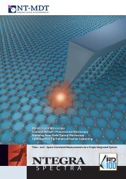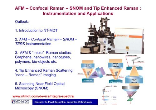
AFM – Confocal Raman – SNOM and Tip Enhanced Raman ...
AFM – Confocal Raman – SNOM and Tip Enhanced Raman ...
AFM – Confocal Raman – SNOM and Tip Enhanced Raman ...

Create successful ePaper yourself
Turn your PDF publications into a flip-book with our unique Google optimized e-Paper software.
<strong>AFM</strong> – <strong>Confocal</strong> <strong>Raman</strong> – <strong>SNOM</strong> <strong>and</strong> <strong>Tip</strong> <strong>Enhanced</strong> <strong>Raman</strong> :<br />
Instrumentation <strong>and</strong> Applications<br />
Outlook:<br />
11. Introduction to NT NT-MDT MDT<br />
2. <strong>AFM</strong> – <strong>Confocal</strong> <strong>Raman</strong> – <strong>SNOM</strong> –<br />
TERS iinstrumentation t t ti<br />
3. <strong>AFM</strong> & “micro”- <strong>Raman</strong> studies:<br />
Graphene, nanowires, nanotubes,<br />
polymers, bio-objects etc.<br />
4. <strong>Tip</strong> <strong>Enhanced</strong> <strong>Raman</strong> Scattering:<br />
“nano – <strong>Raman</strong>” imaging<br />
5. Scanning Near Field Optical<br />
Microscopy (<strong>SNOM</strong>)<br />
www.ntmdt.com/device/ntegra-spectra<br />
Contact: Contact : Dr. Pavel Dorozhkin, dorozhkin@ntmdt.com
NT-MDT NT MDT Europe<br />
Eindhoven, NL<br />
NT-MDT America<br />
SSanta t Clara, Cl USA<br />
NT-MDT Basic offices modes worldwide<br />
www.ntmdt.com<br />
NT-MDT Head Office,<br />
Moscow, Russia<br />
Distributors<br />
Sales Representatives<br />
NT-MDT Shanghai<br />
Shanghai, China<br />
NT-MDT S&L<br />
Limerick Limerick, Irel<strong>and</strong>
NT-MDT Product line<br />
NANOFABs N NO s<br />
NanoLabs<br />
Ed Educations ti<br />
Accessories<br />
• More than 20 years on the SPM/<strong>AFM</strong> market<br />
y<br />
• More than 2400 SPM installations Worldwide<br />
• Offices: Moscow, Eindhoven, Limerick, San-Francisco, Shanghai
SPM modes:<br />
<strong>AFM</strong> (contact, intermittent contact), STM
ALL major <strong>AFM</strong> modes are integrated with RAMAN<br />
NT-MDT St<strong>and</strong>ard Measuring modes<br />
More than 30 possible different <strong>AFM</strong> modes<br />
INTEGRATED with <strong>Raman</strong>-<strong>Confocal</strong><br />
• STM<br />
• Contact <strong>AFM</strong><br />
• Lateral Force Microscopy<br />
• Resonant Mode -Semicontact<br />
• Noncontact <strong>AFM</strong> mode<br />
• Phase Imaging<br />
• Force Modulation (viscoelastisity)<br />
• Magnetic force Microcopy<br />
• Electrostatic Force Microscopy<br />
• Adhesion Force Imaging<br />
• <strong>AFM</strong> Lithography-Force<br />
• Spreading Resistance Imaging (SRI) in Currents 30fA-50nA<br />
• <strong>AFM</strong> Nanolitogrphy (voltage <strong>and</strong> scratching)<br />
• SScanning Capacitance C Imaging (SC (SCI) ) ( (dC/dZ, C/ dC/dV) C/ )<br />
• Scanning Kelvin probe microscopy (SKM)<br />
• Force distance curves<br />
• Force Volume<br />
• NNanomanipulation i l ti<br />
• Piezoresponce Mode<br />
• Sample heating for in-situ melting<br />
• I/V spectroscopy, I(Z) spectroscopy etc.<br />
• El Electrochemistry<br />
t h i t<br />
• <strong>SNOM</strong><br />
• ….<br />
SPM PROBES:<br />
- <strong>AFM</strong> cantilever (any type)<br />
- STM<br />
- tuning fork (shear force)<br />
- tuning fork (normal force)
Inverted<br />
UUpright i ht
<strong>SNOM</strong><br />
ONE SPM BASEMENT & CONTROLLER –<br />
DIFFERENT INSTRUMENTS<br />
<strong>AFM</strong> + STM<br />
NT-MDT SPM’s abilities<br />
<strong>AFM</strong> - <strong>Confocal</strong> <strong>Raman</strong> -<br />
<strong>SNOM</strong> (UPRIGHT)<br />
<strong>AFM</strong> - <strong>Confocal</strong> <strong>Raman</strong> - <strong>SNOM</strong> (INVERTED)
NTEGRA Spectra<br />
Inverted microscope setup (for transparent samples)<br />
“<strong>AFM</strong> + <strong>SNOM</strong> + 3D confocal <strong>Raman</strong> microscope + TERS” system<br />
Lasers<br />
NTEGRA universal<br />
SPM platform<br />
Inverted microscope<br />
(Olympus (Olympus, Nikon …)<br />
)<br />
NTEGRA Spectra<br />
<strong>AFM</strong>-head<br />
<strong>Raman</strong> unit (NT-MDT) (NT MDT)<br />
Sample scanning stage<br />
(100x,1.4 NA objective inside)
NTEGRA Spectra in Upright setup<br />
“<strong>AFM</strong> + <strong>SNOM</strong> + 3D confocal <strong>Raman</strong> microscope + TERS”<br />
system for non-transparent samples<br />
NTEGRA Spectra<br />
<strong>Raman</strong> unit (Renishaw)<br />
Optical <strong>AFM</strong>-head<br />
with integrated 100x objective<br />
Sample scanner<br />
NTEGRA universal<br />
SPM platform
Combination of <strong>AFM</strong> with <strong>Raman</strong><br />
<strong>Confocal</strong><br />
<strong>Raman</strong>:<br />
imaging <strong>and</strong><br />
spectroscopy<br />
<strong>Confocal</strong><br />
fluorescence:<br />
iimaging i <strong>and</strong> d<br />
spectroscopy<br />
NTEGRA Spectra<br />
One object j – many y techniques q<br />
Atomic-force<br />
microscopy:<br />
mechanical,<br />
electrical, magnetic<br />
properties p p <strong>and</strong><br />
nanomanipulations<br />
<strong>Tip</strong> <strong>Enhanced</strong> <strong>Raman</strong> <strong>and</strong><br />
Fluorescence microscopy<br />
Near-field<br />
optical<br />
microscopy i<br />
Optical (white light)<br />
microscopy <strong>and</strong><br />
reflected laser<br />
confocal imaging<br />
Measurements in air, in liquid or in a controlled environment<br />
NTEGRA Spectra<br />
NTEGRA Spectra
NTEGRA Spectra<br />
NTEGRA Spectra<br />
<strong>Confocal</strong> <strong>Raman</strong>/Fluorescence - critical resolution
Resolution test: features 200 nm apart are clearly resolved<br />
<strong>Raman</strong> map measurement parameters:<br />
Objective: 100x, oil immersion<br />
Laser: 473 nm, Grating: 150 lines/mm<br />
Exposure time 0.3 sec<br />
Spectra per sec: >3<br />
PPoint i t number: b 200 200x200 200 pix<br />
i<br />
Sample: p Mineralic toothpaste p<br />
Resolution: < 200 nm<br />
Line #1, Integral intensity<br />
200 nm<br />
300 nm
Very high spectral resolution by Echelle grating<br />
Measurement parameters<br />
Laser: 473 nm<br />
Objective: 100x, 0.95 NA<br />
Grating: Echelle<br />
Actual pixels p of CCD camera are plotted p<br />
(26 µm pixel size)<br />
Spectral resolution:<br />
0281/cm(pixel 0.28 1/cm (pixel to pixel) for 473 nm laser<br />
0.11 1/cm (pixel to pixel) for 785 nm laser<br />
Si line, 1 st order
3D <strong>Raman</strong> mapping, Polystyrene microspheres<br />
X,Y - resolution: 200 nm<br />
Z – resolution: 500 nm<br />
10100<br />
1/cm<br />
3D <strong>Raman</strong> image<br />
XY cross-section<br />
scan size 10x10x14 µm µ
NTEGRA Spectra<br />
Upright configuration for <strong>AFM</strong> – <strong>Confocal</strong> <strong>Raman</strong> – TERS<br />
U i i t ti f<strong>AFM</strong> ith<br />
Unique integration of <strong>AFM</strong> with<br />
high resolution optical microscopy <strong>and</strong> spectroscopy
<strong>AFM</strong> with 100x 0.7 NA objective in upright configuration –<br />
for non-transparent samples<br />
Laser<br />
input&scanning<br />
module d l<br />
NTEGRA Spectra<br />
Probe<br />
deflectometer<br />
Optical <strong>AFM</strong> head<br />
(100x,0.7 NA<br />
objective inside)<br />
CCD video camera<br />
Imaging optics<br />
Beam splitter p 2<br />
Beam splitter 1<br />
<strong>AFM</strong> probe<br />
XYZ scanner<br />
NA=0.7<br />
400 nm resolution<br />
Excitation light<br />
Scattered light<br />
Laser<br />
deflectometer<br />
Sample<br />
objective
<strong>AFM</strong> cantilever under 100x objective (in upright geometry)<br />
Cantilever<br />
<strong>AFM</strong> Optical Image<br />
1 µm height letters are<br />
readable – thanks to<br />
100x objective<br />
(see next slide for <strong>AFM</strong>)<br />
Black spot at the apex of<br />
cantilever is the exact<br />
point there the tip<br />
touches substrate !!!<br />
<strong>AFM</strong> probe over a structured Si substrate.<br />
View through 0.7N 100x objective, resolution 400 nm<br />
Apex of opaque Si tip looks transparent on the image<br />
This unique observation is due to high aperture (0.7 NA) of the imaging objective<br />
NTEGRA Spectra
NTEGRA Spectra<br />
<strong>AFM</strong> – <strong>Confocal</strong> <strong>Raman</strong> “classical applications”<br />
Stress in Silicon<br />
Sili Silicon nanowires i<br />
Carbon nanotubes<br />
GGraphene h<br />
Bio objects<br />
…
Mapping stress in Si by spectral shift of 520 cm -1 line<br />
Stress distribution around nanoindentation in Silicon substrate<br />
<strong>AFM</strong> topography of indentation in<br />
silicon substrate<br />
σ(MPa) = -435 ∆ω (1/cm)<br />
NTEGRA Spectra<br />
Scan size: s 12xx12<br />
microon<br />
0.5 1/ cm<br />
Center of mass position shift of 520 1/cm silicon<br />
line – proportional to stress distribution around<br />
the indentation.<br />
Spectral resolution: better then 0.1 1/cm
Si nanowire – snapshot from the experiment<br />
cantilever apex<br />
cantilever cantilever<br />
nanowire<br />
nanowire laser spot<br />
NTEGRA Spectra + Renishaw <strong>Raman</strong> microscope
Si nanowire - comprehensive characterization in one<br />
sample p scan<br />
Optical image<br />
<strong>AFM</strong> topography<br />
<strong>Raman</strong> map (main Si b<strong>and</strong>)<br />
_____ 5 µm _____ 5 µm<br />
<strong>Raman</strong> map, Si b<strong>and</strong><br />
center of mass position<br />
_____ 5 µm _____ 5 µm<br />
Fluorescence map <strong>Raman</strong> map<br />
(Si nanoparticles b<strong>and</strong>)<br />
_____ 5 µm<br />
Stressed Si<br />
Pristine Si<br />
Si nanoparticles<br />
NT-MDT NTEGRA Spectra + Renishaw <strong>Raman</strong> microscope
Sample: SWCNs, <strong>Raman</strong> spectrum of nanotube bundle<br />
Grating: 600 lines/mm<br />
RBM D<br />
NTEGRA Spectra<br />
G +<br />
G -<br />
Laser: 473 nm<br />
2D
Intensity distribution of different <strong>Raman</strong> b<strong>and</strong>s &<br />
<strong>AFM</strong> topography image of individual NT bundle<br />
RBM-b<strong>and</strong> D-b<strong>and</strong> G - - b<strong>and</strong> G + - b<strong>and</strong><br />
<strong>AFM</strong> height g <strong>AFM</strong> phase<br />
Integration time: 100 ms / point. 50*150 points.<br />
Total spectrum was acquired at each point of the scan. After measurement, different <strong>Raman</strong><br />
b<strong>and</strong>s are chosen <strong>and</strong> their intensity distribution is analyzed. All the images (<strong>AFM</strong> + all <strong>Raman</strong><br />
maps) can obtained simultaneously, simultaneously in a single experiment experiment, without any moving of the sample<br />
or objective<br />
NTEGRA Spectra
2 nm<br />
Sensing individual SWNTs on Si substrate<br />
Spectral integration time at 1 point : 100 msec<br />
E (Horizontal pol.)<br />
E (vertical pol.)<br />
Topography <strong>Raman</strong> map (G-b<strong>and</strong>)
NTEGRA Spectra p<br />
<strong>AFM</strong> – <strong>Confocal</strong> <strong>Raman</strong> of Graphene
Lateral Force Microscopy<br />
Graphene, <strong>AFM</strong> + <strong>Confocal</strong> <strong>Raman</strong><br />
One experiment - multiple data<br />
Electrostatic Force<br />
Force Modulation Microscopy<br />
Microscopy<br />
Capacitance<br />
Microscopy<br />
<strong>Raman</strong> Map, Mass Center of<br />
2D (G’) B<strong>and</strong><br />
<strong>AFM</strong> Topography, Size: 30*30 µm<br />
Scanning Kelvin Probe<br />
Microscopy<br />
R<strong>Raman</strong> MMap, GG-b<strong>and</strong> b d<br />
Intensity<br />
<strong>Confocal</strong> Rayleigh<br />
Microscopy<br />
Data from: E. Kuznetsov,<br />
S. Timofeev, P. Dorozhkin, NT-MDT Co.
HIGH RESOLUTION <strong>AFM</strong> & STM<br />
The high-resolution <strong>AFM</strong> image showing<br />
an assembly of single-layer,<br />
functionalized Graphene sheets sheets.<br />
Some of the sheets are many square<br />
micrometers large. The thickness of each<br />
Atomic resolution STM image of graphite<br />
(HOPG)<br />
sheet is less than 1 nm. Image courtesy:<br />
Dr. Hannes Schniepp (The College of William & Mary, USA)
Nanowire<br />
Light Transport studies with NTEGRA Spectra<br />
Fibeer<br />
probe<br />
(X,YY,Z<br />
scan)<br />
EExcitation it ti points i t<br />
Laser excitation B<br />
Edge filter<br />
Collected light<br />
<strong>AFM</strong> A probe (X,Y,Z scan)<br />
Detection point<br />
Sample (on X,Y,Z-stage)<br />
High NA 100x objective<br />
(Z-movable)<br />
Laser excitation A<br />
X,Y,Z-movable objective<br />
Pinhole: adjustable (0-2 mm) & X,Y-movable<br />
NTEGRA Spectra<br />
To light registration:<br />
Excitation point<br />
`<br />
Emission from ends<br />
Emission from end<br />
Excitation point
Emission from end<br />
Light Transport studies with NTegra Spectra<br />
Excitation point<br />
NNanowire i iis llocally ll excited it d at t the th bbottom tt end. d RRed d curve shows h<br />
fluorescence spectrum taken at the excitation point. Blue curve is the<br />
transmitted light spectrum taken at the upper end of the nanowire. Green<br />
curve shows spectral transmission function of the nanowire<br />
NTEGRA Spectra
Beta-carotene distribution in algal cells<br />
Optical image <strong>Confocal</strong> Laser <strong>AFM</strong> topography<br />
Sample courtesy of Don McNaughton,<br />
Monash University, Australia<br />
NTEGRA Spectra<br />
β-carotene <strong>Raman</strong> b<strong>and</strong><br />
Tail of luminescence<br />
(centered at ~630 630 nm)
Beta-carotene distribution in algal cells<br />
Optical microscope image<br />
(with 100x objective)<br />
Image size:<br />
25x25 µm<br />
<strong>Confocal</strong> laser image <strong>AFM</strong>-image<br />
<strong>Raman</strong> map (ß-carotene) Luminescence map<br />
NTEGRA Spectra<br />
Magnetic Magnetic-,<br />
Kelvin-,<br />
Electrostatic-<br />
Acoustic Force- Force<br />
Capacitance –<br />
Spreading resistance …<br />
Scanning Probe images
Malaria infected red blood cell, <strong>AFM</strong>-<strong>Raman</strong><br />
<strong>AFM</strong> topography <strong>Raman</strong> map<br />
C <strong>Raman</strong> spectra<br />
Hemozoin Hemoglobin<br />
<strong>AFM</strong> image of a trophozoite iRBC <strong>and</strong> a false color 3-cluster UHCA map of the same cell generated from<br />
the <strong>Raman</strong> spectra. Mean cluster spectra from the two clusters associated with hemozoin (blue) <strong>and</strong><br />
hemoglobin (green) are shown. This fixation protocol preserved the structural integrity of the iRBC <strong>and</strong><br />
sub-micron sized knobs can be seen on the surface of the cell in the <strong>AFM</strong> image.<br />
The size of these knobs were 20-50 nm in height <strong>and</strong> 100-150 nm in width which is the same as values<br />
previously reported <strong>and</strong> measured by SEM, TEM, <strong>and</strong> <strong>AFM</strong>.<br />
NTEGRA Spectra Data courtesy: Don MacNaughton, Monash Univ.
Polymer sample with protective cover layer - depth profile<br />
<strong>Raman</strong> spectrum versus sample depth<br />
Sample<br />
deepth,<br />
�m<br />
<strong>Raman</strong> shift<br />
Two layers are observed.<br />
The 2nd layer is 500 nm below the first layer<br />
<strong>and</strong> has a characteristic <strong>Raman</strong> line (620 cm<br />
NTEGRA Spectra<br />
-1 )<br />
Layer #2<br />
Layer #1<br />
Zoomed region<br />
0.5 �m
<strong>AFM</strong> -><br />
Scan size: 40 x 40 µm<br />
<strong>Raman</strong> -><br />
Polymer blend<br />
NT-MDT NTEGRA Spectra + Renishaw <strong>Raman</strong> microscope
NT-MDT + Renishaw INTEGRATED system<br />
Advertising leaflets of the Integrated system (issued by Renishaw <strong>and</strong> by NT-MDT)
NT-MDT + Renishaw INTEGRATED software<br />
1. Renishaw measurement setup<br />
menu is opened <strong>and</strong><br />
controlled from NT-MDT NT MDT<br />
NOVA software<br />
2. NT-MDT software FULLY<br />
controls the <strong>AFM</strong>-<strong>Raman</strong><br />
experiment (except rare<br />
adjustments j or calibrations of<br />
the system)<br />
NTEGRA Spectra
NT-MDT + Renishaw INTEGRATED software<br />
EXACTLY THE SAME DATA in two programs: NT-MDT & Wire-3<br />
All scans can be seen <strong>and</strong> analyzed in any software: <strong>AFM</strong> (height, phase etc) & <strong>Raman</strong><br />
maps. Data from NT-MDT Nova was exported into WIRE-3
<strong>Tip</strong> <strong>Enhanced</strong> <strong>Raman</strong> Scattering (TERS)<br />
A route to <strong>Raman</strong> microscopy py with subwavelength g spatial p<br />
resolution <strong>and</strong> single molecule sensitivity<br />
TERS – “inverted” SERS effect (scanning metal tip is a HOT SPOT)<br />
Electromagnetic field<br />
intensity around<br />
metal tip<br />
2RR)<br />
NTEGRA Spectra<br />
200-600 nm<br />
Metal <strong>AFM</strong> probe<br />
<strong>Enhanced</strong> <strong>Raman</strong><br />
signal<br />
Focused laser spot
NT-MDT provides all possible <strong>AFM</strong>/<strong>Raman</strong>/TERS configurations<br />
INVERTED UPRIGHT Side illumination + UPRIGHT<br />
excitation<br />
TERS collection<br />
TERS collection<br />
excitation<br />
TERS collection E<br />
excitation<br />
Different probe types <strong>and</strong> feedback mechanisms:<br />
<strong>AFM</strong> (contact, intermittent contact), STM, Tuning fork (normal force <strong>and</strong> shear force)<br />
Dual scan: 6 piezodriven coordinates (“laser + sample” or “tip + sample”)
<strong>Tip</strong> <strong>Enhanced</strong> <strong>Raman</strong><br />
INVERTED geometry (transparent samples)<br />
Sh Shear fforce
To find HOT POINT (Maximum enhancement):<br />
Scan - BY TIP; Measure - intensity of laser light scattered by the tip<br />
E<br />
200 nm ____<br />
HHot t point i t !<br />
Metal <strong>AFM</strong> probe<br />
xy&z-scan<br />
x,y & z scan<br />
Focused laser spot<br />
Etched Au wire<br />
1. Scan (XY&Z) by tip across<br />
the laser spot. p<br />
Measure <strong>Raman</strong> or Rayleigh<br />
scattered light<br />
2. Position tip inside “hot point”<br />
with high precision<br />
Scan by the sample to get<br />
TERS map<br />
Data courtesy of S. Kharintsev, J. Loos, G. Hoffman, G. de With, TUE, the Netherl<strong>and</strong>s <strong>and</strong> P. Dorozhkin, NT-MDT
TERS imaging of single-walled CNT bundle<br />
__ 200 nm<br />
<strong>Tip</strong> is away<br />
__ 200 nm<br />
Tube image width<br />
<strong>AFM</strong> topography<br />
is<br />
(h (height i<br />
~250<br />
ht<br />
250<br />
~ 5<br />
nm<br />
nm) )<br />
(limited by<br />
wavelength of light)<br />
<strong>Raman</strong> map<br />
(G-line)<br />
<strong>Tip</strong> p is approached<br />
pp<br />
Laser: 633 nm<br />
Tube image width is<br />
<strong>Tip</strong>: Etched gold wire ~50 nm (limited (<br />
only by size of the tip)<br />
S.S. Kharintsev, G. Hoffmann, P.S. Dorozhkin,<br />
G. de With, <strong>and</strong> J. Loos<br />
Nanotechnology 18 (2007), 315502<br />
<strong>Raman</strong> spectra <strong>and</strong> 2D confocal <strong>Raman</strong> maps (G (G-line) line) of carbon nanotube<br />
rope with <strong>and</strong> without enhancing <strong>AFM</strong> tip (GOLD wire)<br />
NTEGRA Spectra
TERS with Silver coated cantilevers<br />
<strong>AFM</strong> image of carbon nanotube<br />
bundle<br />
Scan size: 2x3 micron<br />
TERS image of the same<br />
bundle<br />
Image courtesy: Jacon Jao, Jao Renato Zenobi ETH Zurich, Zurich Switzerl<strong>and</strong>; GG.<br />
Hoffman, J. Loos, TUE, Eindhoven; <strong>and</strong> Pavel Dorozhkin, NT-MDT Russia<br />
NTEGRA Spectra<br />
`
<strong>Tip</strong> <strong>Enhanced</strong> <strong>Raman</strong><br />
UPRIGHT geometry t (non-transparent ( t t samples) l )<br />
100x<br />
0.7 NA<br />
TERS excitation<br />
TERS collection<br />
0.7 NA<br />
45°<br />
100 100x TERS collection ll ti<br />
0.7 NA<br />
E<br />
excitation
Looking for Hot Spot –<br />
laser beam is scanned across the cantilever<br />
0.7 NA<br />
45°<br />
Laser scanning module allows to position laser beam precisely at the apex of <strong>AFM</strong><br />
tip <strong>and</strong> fix it there - thanks to closed-loop operation of the scanning mirror
TERS in UPRIGHT geometry – Graphene<br />
Finding g HOT SPOT on <strong>AFM</strong> tipp<br />
<strong>Raman</strong> spectra from Graphene flake:<br />
--- Inside “hotspot”<br />
--- Outside “hotspot” hotspot<br />
--- Signal from tip (sample is removed)<br />
Data from: A. Schokin &<br />
PP. Dorozhkin Dorozhkin, NT‐MDT<br />
Laser beam is scanned across cantilever tip<br />
<strong>Raman</strong> signal from substrate measured<br />
cantilever
TERS on periodic Si-Ge structure, resolution ~50 nm<br />
Data courtesy: Dr. Peter Hermann et at., Fraunhofer CNT & AMD, Dresden<br />
TERS tool evaluation project, AMD Dresden & NT-MDT
Successful <strong>Tip</strong> <strong>Enhanced</strong> <strong>Raman</strong> experiment:<br />
Major requirements to experimental setup (<strong>AFM</strong> – <strong>Raman</strong> combination)<br />
1. Different geometry of <strong>AFM</strong> <strong>and</strong> high resolution <strong>Raman</strong> optics: bottom<br />
illumination/collection, top illumination/collection, side illumination/ top<br />
collection.<br />
2. Dual scan option (6 closed loop piezo coordinates): sample+laser<br />
scanning OR sample+tip scanning<br />
3. All <strong>AFM</strong> <strong>and</strong> <strong>Raman</strong> control must be integrated into one software package<br />
4. Very y low <strong>AFM</strong> noise (to ( keep p TERS tip p safely y very y<br />
close to sample), low drifts <strong>and</strong> high stability<br />
(to keep laser exactly on the hot<br />
spot p – with 10 nm precision) p )<br />
5. Good TERS tip
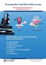
SCANNING NEAR-FIELD OPTICAL MICROSCOPY<br />
Straight quartz fiber with<br />
aperture (glued to tuning fork)<br />
Silicon cantilevers with<br />
aperture<br />
100x, 0.7 NA<br />
All <strong>SNOM</strong> modes are available:<br />
Collection, Transmission, Reflection<br />
(for all signals/modes: laser, fluorescence <strong>and</strong> spectroscopy)
AUTOMATIC alignment of laser spot <strong>and</strong> <strong>SNOM</strong> aperture<br />
laser spot is scanned: xx,y y Intensity of light transmitted<br />
through cantilever<br />
Precise location of <strong>SNOM</strong> aperture<br />
___ 10µm<br />
Laser spot is scanned in automatic regime across <strong>SNOM</strong> cantilever <strong>and</strong> transmitted<br />
signal is measured – to locate the <strong>SNOM</strong> aperture with very high accuracy (
<strong>SNOM</strong> transmission: Single lipofuscin granule<br />
Shear force topography <strong>SNOM</strong> transmission<br />
Single lipofuscin granule 400 nm in height <strong>and</strong> 1.7 – 2.7 µm in<br />
diameter. Two “humps” can be seen as well at shear-force image<br />
(left one). one) On the right image transmission at 420 nm can be seen seen.<br />
Quartz substrate transmission was subtracted so negative values can<br />
be referred to sample absorption <strong>and</strong> positive ones (most probably)<br />
to sample fluorescence.<br />
NTEGRA Spectra
<strong>SNOM</strong> spectroscopy: Single lipofuscin granule<br />
Point-localized spectroscopy of putative fluorescent region. The<br />
spectrum obtained corresponds well with the spectrum of pure<br />
A2E fluorophore thought to be the major cause of aging-related<br />
retina degeneration<br />
degeneration.<br />
NTEGRA Spectra
<strong>SNOM</strong> on photonic <strong>SNOM</strong> Lithography crystal performance optical fibers<br />
NTEGRA Spectra<br />
Overlay of simultaneously measured:<br />
Sample topography (orange/red palette) <strong>and</strong><br />
<strong>SNOM</strong> intensity (green palette)<br />
Data courtesy:<br />
Yinlan Ruan, Heike Ebendorff-Heidepriem, Tanya M. Monro<br />
Centre of Expertise in Photonics Photonics, School of Chemistry &<br />
Physics, University of Adelaide, Adelaide, 5000 Australia
<strong>SNOM</strong> measurements (VIS & IR) : Cr:YAG optical fibers
<strong>SNOM</strong> on Surface Plasmon Polaritons<br />
Data from:<br />
Antonell Nesci <strong>and</strong> Olivier J.F. Martin,<br />
EPFL, Lausanne, Switzerl<strong>and</strong>
<strong>SNOM</strong> on Surface Plasmon Polaritons<br />
Data from:<br />
Antonell Nesci <strong>and</strong> Olivier JJ.F. F Martin Martin,<br />
EPFL, Lausanne, Switzerl<strong>and</strong>
NTEGRA Spectra<br />
NTEGRA Spectra<br />
<strong>AFM</strong> – <strong>Raman</strong> – <strong>SNOM</strong> in controlled environment
<strong>SNOM</strong><br />
<strong>AFM</strong> + <strong>Raman</strong> + <strong>SNOM</strong> in LIQUID<br />
<strong>AFM</strong><br />
NT-MDT Closed-liquid cell with heating<br />
Possible to use with <strong>AFM</strong> + <strong>SNOM</strong> + <strong>Confocal</strong> <strong>Raman</strong> (<strong>Confocal</strong><br />
fluorescence), ), work with living g cells. Flow-trough g ppossibility. y<br />
WORKS WITH <strong>AFM</strong>/<strong>SNOM</strong>/ RAMAN (INVERTED)<br />
NTEGRA Spectra
<strong>AFM</strong> – <strong>Raman</strong> – <strong>SNOM</strong> in Upright configuration in liquid<br />
100x<br />
100x<br />
NA = 1<br />
NA = 1<br />
280 nm<br />
- NA=1 (120º)<br />
2 mm<br />
280 nm<br />
- TERS in liquid for opaque samples<br />
- Cantilever based <strong>SNOM</strong> in liquid
Electrochemical cell for <strong>AFM</strong> – <strong>Raman</strong> in external magnetic field<br />
<strong>AFM</strong> quartz nose<br />
EC cell<br />
Transparent sample<br />
Cantilever<br />
objective<br />
• Microscope configuration: Inverted<br />
• Objectives used: any objective (Olympus,<br />
Nikon)<br />
• <strong>AFM</strong> modes in liquid: contact, noncontact<br />
• Sample: transparent (ITO, quartz with<br />
thin metal layer etc.)<br />
• Stabilized temperature p (-10º ( - +60º) )<br />
• External magnetic field (up to 0.2 T)<br />
NTEGRA Spectra<br />
EC cell<br />
objective
Ultra Stable <strong>AFM</strong> – <strong>Confocal</strong> <strong>Raman</strong> – TERS measurements<br />
in wide temperature range<br />
T = -30 - +80 ºC<br />
Drifts < 10 nm per 1ºC 1C < 10 nm per hour at all temperatures<br />
Couunts<br />
3000<br />
2750<br />
2500<br />
2250<br />
2000<br />
1750<br />
1500<br />
1250<br />
1000<br />
750<br />
500<br />
<strong>Raman</strong> spectra of Graphene<br />
flake at T = -20, , +20, , +80 ºC<br />
<strong>Raman</strong> spectrums vs temperature<br />
T=25 C<br />
T= 80 C<br />
T= -20 C<br />
1400 1800 2200 2600 3000<br />
1200 1600 2000 2400 2800 3200<br />
<strong>Raman</strong> shift, cm-1
<strong>AFM</strong>-<strong>Raman</strong>-<strong>SNOM</strong>-TERS in CONTROLLED ATMOSPHERE<br />
Controlled atmosphere chamber for <strong>AFM</strong>-<strong>Raman</strong>-TERS<br />
(controlled temperature, humidity, inert gases etc.)<br />
NTEGRA Spectra
Modes<br />
NT MDT integrates<br />
<strong>AFM</strong>, <strong>SNOM</strong>, <strong>Confocal</strong> <strong>Raman</strong>/Fluorescence <strong>and</strong> TERS<br />
in one device<br />
• <strong>AFM</strong> (mechanical, electrical, magnetic properties<br />
<strong>and</strong> nanomanipulation – more than 30 modes)<br />
• White Light Microscopy <strong>and</strong> Reflected Laser<br />
(Rayleigh) <strong>Confocal</strong> Imaging<br />
• <strong>Confocal</strong> <strong>Raman</strong> Imaging <strong>and</strong> Spectroscopy<br />
• <strong>Confocal</strong> Fluorescence Imaging g g <strong>and</strong><br />
Spectroscopy<br />
• Scanning Near-Field Optical Microscopy<br />
• <strong>Tip</strong> <strong>Enhanced</strong> <strong>Raman</strong> <strong>and</strong> Fluorescence<br />
Microscopy (TERS, TEFS)<br />
www.ntmdt.com/device/ntegra-spectra<br />
Controlled environment<br />
•Temperature<br />
•Humidity<br />
•Gases<br />
•Liquid<br />
•Electrochemical environment<br />
•External magnetic field<br />
Contact : Dr. Pavel Dorozhkin, dorozhkin@ntmdt.com